EP1542063A1 - Optical modulator - Google Patents
Optical modulator Download PDFInfo
- Publication number
- EP1542063A1 EP1542063A1 EP03795353A EP03795353A EP1542063A1 EP 1542063 A1 EP1542063 A1 EP 1542063A1 EP 03795353 A EP03795353 A EP 03795353A EP 03795353 A EP03795353 A EP 03795353A EP 1542063 A1 EP1542063 A1 EP 1542063A1
- Authority
- EP
- European Patent Office
- Prior art keywords
- recess
- optical modulator
- substrate
- electrode
- stress
- Prior art date
- Legal status (The legal status is an assumption and is not a legal conclusion. Google has not performed a legal analysis and makes no representation as to the accuracy of the status listed.)
- Granted
Links
- 230000003287 optical effect Effects 0.000 title claims abstract description 141
- 239000000758 substrate Substances 0.000 claims abstract description 67
- 230000002040 relaxant effect Effects 0.000 claims abstract description 23
- 230000000694 effects Effects 0.000 claims abstract description 15
- 239000000463 material Substances 0.000 claims abstract description 9
- 239000013078 crystal Substances 0.000 claims description 8
- 230000006866 deterioration Effects 0.000 abstract description 3
- 230000001747 exhibiting effect Effects 0.000 abstract 1
- GQYHUHYESMUTHG-UHFFFAOYSA-N lithium niobate Chemical compound [Li+].[O-][Nb](=O)=O GQYHUHYESMUTHG-UHFFFAOYSA-N 0.000 description 14
- 238000000034 method Methods 0.000 description 13
- 239000010931 gold Substances 0.000 description 10
- VYPSYNLAJGMNEJ-UHFFFAOYSA-N Silicium dioxide Chemical compound O=[Si]=O VYPSYNLAJGMNEJ-UHFFFAOYSA-N 0.000 description 9
- 230000005540 biological transmission Effects 0.000 description 8
- 238000007747 plating Methods 0.000 description 7
- PCHJSUWPFVWCPO-UHFFFAOYSA-N gold Chemical compound [Au] PCHJSUWPFVWCPO-UHFFFAOYSA-N 0.000 description 6
- 229910052737 gold Inorganic materials 0.000 description 6
- 230000015572 biosynthetic process Effects 0.000 description 5
- 230000005684 electric field Effects 0.000 description 5
- 238000004519 manufacturing process Methods 0.000 description 5
- 229910052681 coesite Inorganic materials 0.000 description 4
- 238000004891 communication Methods 0.000 description 4
- 229910052906 cristobalite Inorganic materials 0.000 description 4
- 238000009792 diffusion process Methods 0.000 description 4
- 238000005516 engineering process Methods 0.000 description 4
- 239000000377 silicon dioxide Substances 0.000 description 4
- 229910052682 stishovite Inorganic materials 0.000 description 4
- 229910052905 tridymite Inorganic materials 0.000 description 4
- 229910003327 LiNbO3 Inorganic materials 0.000 description 3
- 229910012463 LiTaO3 Inorganic materials 0.000 description 3
- 230000008021 deposition Effects 0.000 description 2
- 238000010586 diagram Methods 0.000 description 2
- 238000005530 etching Methods 0.000 description 2
- 238000011156 evaluation Methods 0.000 description 2
- 230000002349 favourable effect Effects 0.000 description 2
- 239000000835 fiber Substances 0.000 description 2
- 229920002120 photoresistant polymer Polymers 0.000 description 2
- WHXSMMKQMYFTQS-UHFFFAOYSA-N Lithium Chemical compound [Li] WHXSMMKQMYFTQS-UHFFFAOYSA-N 0.000 description 1
- RTAQQCXQSZGOHL-UHFFFAOYSA-N Titanium Chemical compound [Ti] RTAQQCXQSZGOHL-UHFFFAOYSA-N 0.000 description 1
- 230000009286 beneficial effect Effects 0.000 description 1
- 239000012141 concentrate Substances 0.000 description 1
- 238000010276 construction Methods 0.000 description 1
- 230000003247 decreasing effect Effects 0.000 description 1
- 230000001687 destabilization Effects 0.000 description 1
- 238000001312 dry etching Methods 0.000 description 1
- 230000005685 electric field effect Effects 0.000 description 1
- 230000003628 erosive effect Effects 0.000 description 1
- 238000001704 evaporation Methods 0.000 description 1
- 229910052746 lanthanum Inorganic materials 0.000 description 1
- FZLIPJUXYLNCLC-UHFFFAOYSA-N lanthanum atom Chemical compound [La] FZLIPJUXYLNCLC-UHFFFAOYSA-N 0.000 description 1
- 229910052744 lithium Inorganic materials 0.000 description 1
- 230000000873 masking effect Effects 0.000 description 1
- 229910052751 metal Inorganic materials 0.000 description 1
- 239000002184 metal Substances 0.000 description 1
- 230000010287 polarization Effects 0.000 description 1
- 230000000644 propagated effect Effects 0.000 description 1
- 239000010453 quartz Substances 0.000 description 1
- 230000007261 regionalization Effects 0.000 description 1
- 239000006104 solid solution Substances 0.000 description 1
Images


Classifications
-
- G—PHYSICS
- G02—OPTICS
- G02F—OPTICAL DEVICES OR ARRANGEMENTS FOR THE CONTROL OF LIGHT BY MODIFICATION OF THE OPTICAL PROPERTIES OF THE MEDIA OF THE ELEMENTS INVOLVED THEREIN; NON-LINEAR OPTICS; FREQUENCY-CHANGING OF LIGHT; OPTICAL LOGIC ELEMENTS; OPTICAL ANALOGUE/DIGITAL CONVERTERS
- G02F1/00—Devices or arrangements for the control of the intensity, colour, phase, polarisation or direction of light arriving from an independent light source, e.g. switching, gating or modulating; Non-linear optics
- G02F1/01—Devices or arrangements for the control of the intensity, colour, phase, polarisation or direction of light arriving from an independent light source, e.g. switching, gating or modulating; Non-linear optics for the control of the intensity, phase, polarisation or colour
- G02F1/03—Devices or arrangements for the control of the intensity, colour, phase, polarisation or direction of light arriving from an independent light source, e.g. switching, gating or modulating; Non-linear optics for the control of the intensity, phase, polarisation or colour based on ceramics or electro-optical crystals, e.g. exhibiting Pockels effect or Kerr effect
- G02F1/0305—Constructional arrangements
-
- G—PHYSICS
- G02—OPTICS
- G02F—OPTICAL DEVICES OR ARRANGEMENTS FOR THE CONTROL OF LIGHT BY MODIFICATION OF THE OPTICAL PROPERTIES OF THE MEDIA OF THE ELEMENTS INVOLVED THEREIN; NON-LINEAR OPTICS; FREQUENCY-CHANGING OF LIGHT; OPTICAL LOGIC ELEMENTS; OPTICAL ANALOGUE/DIGITAL CONVERTERS
- G02F1/00—Devices or arrangements for the control of the intensity, colour, phase, polarisation or direction of light arriving from an independent light source, e.g. switching, gating or modulating; Non-linear optics
- G02F1/01—Devices or arrangements for the control of the intensity, colour, phase, polarisation or direction of light arriving from an independent light source, e.g. switching, gating or modulating; Non-linear optics for the control of the intensity, phase, polarisation or colour
- G02F1/03—Devices or arrangements for the control of the intensity, colour, phase, polarisation or direction of light arriving from an independent light source, e.g. switching, gating or modulating; Non-linear optics for the control of the intensity, phase, polarisation or colour based on ceramics or electro-optical crystals, e.g. exhibiting Pockels effect or Kerr effect
- G02F1/0305—Constructional arrangements
- G02F1/0316—Electrodes
-
- G—PHYSICS
- G02—OPTICS
- G02F—OPTICAL DEVICES OR ARRANGEMENTS FOR THE CONTROL OF LIGHT BY MODIFICATION OF THE OPTICAL PROPERTIES OF THE MEDIA OF THE ELEMENTS INVOLVED THEREIN; NON-LINEAR OPTICS; FREQUENCY-CHANGING OF LIGHT; OPTICAL LOGIC ELEMENTS; OPTICAL ANALOGUE/DIGITAL CONVERTERS
- G02F1/00—Devices or arrangements for the control of the intensity, colour, phase, polarisation or direction of light arriving from an independent light source, e.g. switching, gating or modulating; Non-linear optics
- G02F1/01—Devices or arrangements for the control of the intensity, colour, phase, polarisation or direction of light arriving from an independent light source, e.g. switching, gating or modulating; Non-linear optics for the control of the intensity, phase, polarisation or colour
- G02F1/21—Devices or arrangements for the control of the intensity, colour, phase, polarisation or direction of light arriving from an independent light source, e.g. switching, gating or modulating; Non-linear optics for the control of the intensity, phase, polarisation or colour by interference
- G02F1/225—Devices or arrangements for the control of the intensity, colour, phase, polarisation or direction of light arriving from an independent light source, e.g. switching, gating or modulating; Non-linear optics for the control of the intensity, phase, polarisation or colour by interference in an optical waveguide structure
Definitions
- an optical modulator which corresponds to a dense wavelength division multiplexing (DWDM) technology and high speed communication technology
- the optical modulator which modulates a light from CW (Continuous Wave) laser using a Mach-Zehnder (MZ) type external optical modulator (hereinafter described as LN optical modulator) using a material having the electrooptic effect, such as lithium niobate (LN), have been put to practical use.
- MZ Mach-Zehnder
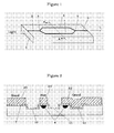
- the MZ type external optical modulator is configured to divide a light inputted from an input optical waveguide 2 in half with a Y-shaped branching optical waveguide 3, to combine the lights guided through two optical waveguides 4 (the optical waveguides, wherein a light guided inside receives a phase control by the electrooptic effect of an electric field formed by a modulating electrode and a grounding electrode, which are control electrodes; hereinafter described as an optical waveguide modulation part) with another Y-shaped branching optical waveguide 5, and to put the modulated light to the exterior via an output optical waveguide 6.
- Each of these optical waveguides is formed by thermal diffusion of a high refractive index material such as Ti, on the surface of a substrate 1 having the electrooptic effect.
- the control electrodes such as the modulating electrode and the grounding electrode formed on the substrate 1 are omitted in order to make the shape of the optical waveguides easily understood.
- Japanese Patent Application No. H10-90638 discloses an optical waveguide with ridge structure.
- Fig.2 is a cross-section view of the MZ type optical modulator shown in Fig.1 along the dashed line A in a direction perpendicular to the optical waveguide modulation part 4.
- 7 in Fig.2 indicates a buffer layer formed from SiO 2 or the like.
- the grounding electrode 22 is formed over the recess 12.
- the temperature mainly around the control electrode section like the grounding electrode rises due to driving of the optical modulator over a long time and an increasing driving power that is inputted into the optical modulator.
- the difference in a coefficient of thermal expansion between the substrate forming the recess 12 and the grounding electrode formed on the recess 12 concentrates stress by the grounding electrode centrally in the side of the recess. Said stress generates stress-strain in the substrate. Since such stress-strain changes the refractive index of the substrate including the optical waveguide, it becomes a big obstacle in stably controlling the phase of light passing through the optical waveguide in the optical modulator.
- the present invention intends to solve the above-described problems, to relax the stress generated in the recess formed in the surface of the substrate in the optical modulator, to inhibit deterioration of optical modulation control caused by the stress-strain in the substrate including the optical waveguide, and to provide the optical modulator which realizes stabilized driving over a long time.
- the invention related to Claim 1 provides an optical modulator comprising a substrate consisting of a material having an electrooptic effect, an optical waveguide provided on said substrate, control electrodes for controlling the phase of light being guided through the optical waveguide, and a recess in the surface of the substrate where the control electrodes are formed, characterized in that the control electrode being formed on said recess is provided with a stress relaxing means.
- the invention related to Clam 2 provides the optical modulator as claimed in Claim 1, characterized in that the stress relaxing means configures said control electrode on the recess thinner than the control electrodes on the non-recess.
- the invention related to Claim 3 is characterized in that the stress relaxing means configures the control electrode on the recess thinner than the depth of the recess.
- control electrode on the recess is configured to be thinner than the control electrodes on the non-recess, it is possible to keep the stress of thermal expansion generated in the control electrode on the recess lower than the stress generated in the control electrodes on the non-recess. Further, because the mechanical strength of the control electrode on the recess is weaker than that of the control electrodes on the non-recess, the stress-strain generated by the control electrodes as a whole can be absorbed by the mechanical deformation of the control electrode on the recess. Then, transmission of the stress from the control electrodes to the surface of the substrate is relaxed. Especially the stress can be prevented from concentrating in the side of the recess.
- control electrode on the recess thinner than the depth of the recess, it becomes possible to localize and lessen the stress that the control electrode on the recess gives on the side of the recess. Moreover, because the control electrode on the recess is weaker than the substrate forming the side of the recess in mechanical strength, the stress on the side of the recess can be further inhibited.
- the invention related to Claim 4 provides the optical modulator as claimed in any of Claims 2 and 3, characterized in that the thickness of the control electrode on the recess is 30000 to 500 ⁇ .
- control electrode thinner than 30000 ⁇ , preferably thinner than 20000 ⁇ , it is adequately thin even compared with a control electrode 20 ⁇ m thick and a ridge part about 4 to 10 ⁇ m deep, which are applied for an average optical modulator. Therefore, the stress that the control electrode on the recess gives on the recess can be inhibited sufficiently.
- control electrode on the recess thicker than 100 ⁇ , preferably thicker than 500 ⁇ , it is possible to ensure the thickness thicker than the film thickness of a conducting line which can be stably produced, in deposition applied for the production process of an optical modulator.
- the invention related to Claim 5 provides the optical modulator as claimed in Claim 1, characterized in that the stress relaxing means creates a space between the substrate surface where the recess is formed and the control electrode on the recess.
- the space is created between the substrate surface where the recess is formed and the control electrode on the recess, to keep the substrate surface and the control electrode out of contact with each other. Therefore the stress of the control electrode is prevented from being given on the substrate surface on the recess, especially on the side of the recess.
- control electrode on the substrate surface providing the recess thinner than the control electrodes on the substrate surface the non-recess. It is more preferable to configure it 1 to 10 ⁇ m in thickness.
- the invention related to Claim 6 provides the optical modulator as claimed in any of Claims 1 to 5, characterized in that the stress relaxing means forms the control electrode on the recess in the shape of a stripe or a lattice.
- control electrode on the recess is in the shape of a stripe or a lattice, even when the control electrode on the recess thermal-expands, it expands to spaces formed by the shape of a stripe or a lattice. It is thereby possible to inhibit stress concentrating in the side of the recess. Moreover, since the part in the shape of a stripe or a lattice has weaker mechanical strength than the other control electrodes, the stress-strain generated by the control electrodes as a whole can be absorbed by the mechanical deformation of the control electrode on the recess. This relaxes transmission of the stress from the control electrodes to the substrate surface. Further, by combining it with any configuration disclosed in Claims 2 to 5, it is possible to inhibit concentration of stress in the side of the recess more effectively.
- the invention related to Claim 7 provides the optical modulator as claimed in Claim 1, characterized in that the stress relaxing means configures the control electrode on the recess to be a thin line for connecting the control electrodes formed on the non-recess next to said recess.
- the thin line connects the control electrodes formed on non-recess next to the recess
- the thin line which is the control electrode on the recess, scarcely generates stress that could influence the optical modulator. Furthermore, because transmission of the stress generated in the control electrodes formed on the non-recess is blocked at the recess, the side of the recess is prevented from receiving the stress.
- the invention related to Claim 8 provides the optical modulator as claimed in any of Claims 1 to 7, characterized in that the substrate comprises the direction of a crystal axis which can change a refractive index in a vertical direction to the substrate surface in the most effective manner by the electrooptic effect.
- the optical modulator comprises the substrate (hereinafter described as Z cut substrate) having the direction of a crystal axis which can change the refractive index in the vertical direction to the substrate surface in the most effective manner by the electrooptic effect
- grooves are sometimes formed on both sides of the optical waveguide such that the grooves sandwich the optical waveguide, for the purpose of performing electrooptic effect of an electric field on the optical waveguide effectively since it is necessary to impress the electric filed in the vertical direction to the substrate surface.
- the technology for providing the stress relaxing means for the control electrode formed on the recess which is disclosed in any of Claims 1 to 7, to such optical modulator having the Z cut substrate, it becomes possible to provide the optical modulator with superior characteristics.
- the invention related to Claim 9 provides the optical modulator as claimed in any of Claims 1 to 8, characterized in that said control electrode is a grounding electrode.
- the construction for providing the control electrode formed on the recess with the stress relaxing means as described in any of Claims 1 to 8 has a discontinuous change in impedance or shape of the control electrode before or after the stress relaxing means, a high-frequency microwave is given to being reflected or radiated to the exterior of the control electrode when it is propagated. Therefore, the characteristics of the optical modulator possibly deteriorate when the control electrode is made as a modulating electrode.
- the control electrode providing the stress relaxing means as the grounding electrode, as in the invention related to Claim 9, it becomes possible to provide the optical modulator with superior characteristics.
- the substrate which configures an optical modulator is made of a material having an electrooptic effect, such as lithum niobate (LiNbO 3 ; hereinafter referred to as LN), lithium tantalite (LiTaO 3 ), PLZT (lead lanthanum zirconate titanate) or quartz-based material.
- LN lithum niobate
- LiTaO 3 lithium tantalite
- PLZT lead lanthanum zirconate titanate
- quartz-based material quartz-based material.
- the present invention embodiments primarily refer to an example using lithium niobate (LN).
- the present invention being explained by the example using a substrate, so-called a Z cut substrate, having the direction of a crystal axis which can change a refractive index in a vertical direction to the substrate surface in the most effective manner by the electrooptic effect, is not limited to the Z cut substrate.
- a buffer layer such as SiO 2 , which is dielectric
- a plurality of optical modulators are fabricated on one LN wafer, which is cut into individual optical modulators at the last stage and thereby, optical modulators are manufactured.
- a MZ type optical modulator as shown in Fig. 1 is explained as the embodiment of the present invention.
- 1 is an LN substrate forming the optical waveguide on its surface by internal diffusion of Ti as above described.
- 2 is an input optical waveguide, where a light is guided from a CW laser light source that is not shown in the figure, and which is connected to a fiber (not shown in the figure) having a polarization maintain feature.
- the light passing through the input optical waveguide 2 is divided in half by a 3dB branching optical waveguide 3, which is a first branching optical waveguide.
- Each divided light enters an optical waveguide modulation part 4 configuring the arms of the Mach-Zehnder optical waveguide.
- Control electrodes comprising a modulating electrode and a grounding electrode, which are not shown in the figure, are formed adjacent to the optical waveguide modulation part 4.
- the light passing through the optical waveguide modulation part 4 in accordance with a signal impressed into the modulating electrode receives phase modulation. After the phase modulation, each guided light is combined and mutually interferes to generate an intensely modulated signal light at a second branching optical waveguide 5.
- the signal light passes through an output optical waveguide 6, and then, is outputted from the optical modulator module through an output fiber which is not shown in the picture.
- grooves are formed adjacent to the optical waveguide modulation part 4 such that the grooves sandwich the optical waveguide modulation part 4. It is configured such that the electric field generated by the modulating electrode and the grounding electrode formed on the optical waveguide modulation part 4 works on the optical waveguide modulation part 4 intensively.
- the grooves are formed by erosion • cutting of the substrate by etching or sandblast etc. before forming the buffer layer such as SiO 2 .
- stress relaxing means which is characteristic of the present invention, provided for the control electrode on a recess is explained.
- Figs. 3 to 5 are diagrams showing the shape of cross section when the optical modulator of the present invention is cut off along the dashed line A in Fig. 1.
- Figs. 4 and 5 show only the shape around the substrate surface.
- Fig. 6 (a) is a perspective view of the shape of cross section when the optical modulator of the present invention is cut off along the dashed line A in Fig. 1.
- Fig. 6 (b), (c) and (d) show the shape of the control electrode formed on the recess when it is seen from above an LN substrate.
- the first embodiment of the present invention shown in Fig.3 is characterized in that, concerning each thickness of electrode sections 23, 24, and 25 which configure one grounding electrode, the grounding electrode section 24 on a recess 12 is configured to be thinner than the grounding electrode sections 23 and 25 on the non-recess, preferably thinner than the depth of the recess 12. This enables remarkable improving of the effect of stress relaxing.
- the specific thickness of the grounding electrode section 24 on the recess 12 is preferably thinner than 30000 ⁇ , more preferably thinner than 20000 ⁇ .
- the thickness of the grounding electrode section 24 is thereby adequately thin even compared with the thickness of the grounding electrode sections 23 and 25 on the non-recess (a control electrode used for an average optical modulator is about 20 ⁇ m in thickness), or with about 10 ⁇ m of the depth of a groove of a ridge part, it becomes possible to prevent the stress generated in the grounding electrode section 24 on the recess and the grounding electrode sections 23 and 25 from concentrating into the side of the recess 12.
- control electrode section 24 on the recess thicker than 100 ⁇ , preferably thicker than 500 ⁇ , it is possible to produce an optical modulator stably without any problem such as disconnection of the grounding electrode section in deposition which is applied for the production process of the optical modulator.
- the second embodiment of the present invention shown in Fig. 4 is characterized in that a space 30 is created between the recess 12 and a grounding electrode section 26. Because this keeps the control electrode away from the recess 12, the stress generated in the grounding electrode sections 23, 25 and 26 is prevented from being put on the side of the recess 12.
- a method for forming a liftoff layer on the recess 12 before the formation of the electrode pattern, and subsequently performing formation of the electrode pattern and a gold plating treatment etc. and then, removing the liftoff layer is cited as a method for producing the above grounding electrode section shown in Fig.4.
- the third embodiment of the present invention shown in Fig.5 is characterized in that the grounding electrode sections 23 and 25 are connected with each other using a conducting wire 27 in the shape of a thin line such as ribbon or wire.
- a conducting wire 27 in the shape of a thin line such as ribbon or wire.
- a method for forming the grounding electrode sections 23 and 25 according to the electrode pattern formation and the gold plating treatment, and subsequently connecting the thin line 7 to each of grounding electrode sections 23 and 25 using wire bonding or the like is cited as a method for producing the grounding electrode sections 23, 25 and 27 shown in Fig.5.
- the fourth embodiment of the present invention shown in Fig.6 is characterized in that the control electrode on the recess is in the shape of a stripe or a lattice.
- the control electrode on the recess is in the shape of a stripe or a lattice.
- stripes are formed in a direction perpendicular to a long side of the recess.
- stripes are inclined to the long side of the recess.
- the control electrode on the recess is in the shape of a lattice.
- lattice is inclined to the long side.
- thermal expansion of the control electrode can be absorbed by spaces formed by the stripe shape or lattice shape, and the stress on the side of the recess can be decreased.
- the part in the shape of a stripe or lattice has weaker mechanical strength than the other parts of the control electrode, the stress-strain generated in the control electrodes as a whole can be absorbed by the mechanical deformation of the control electrode on the recess. Then, transmission of the stress from the control electrodes to the surface of the substrate is relaxed.
- Figs. 6 show straight-line shape, it is also possible to form the control electrode with curved lines such as wavy lines.
- intervals between stripes or lattices are not limited to regular intervals, but can be changed such that, for example, the intervals get dense where the control electrode needs low resistivity, and the intervals get sparse where the control electrode needs high resistivity.
- An optical waveguide was formed by Ti thermal diffusion on an LN substrate with Z cut, and subsequently 0.5 ⁇ m of a buffer layer of SiO 2 was formed on the surface of the substrate.
- the control electrode after forming a Ti layer and an Au layer as a foundation layer by an evaporation method, the Au layer was formed into an electrode of 20 ⁇ m in thickness by a plating method as an electrode layer.
- the cross-section view of the optical modulator formed as described above is in the shape shown in Fig. 2.
- the temperature characteristic of a bias point and a transmission frequency response were measured.
- the DC bias change (drift) amount of the optical modulator was measured in a temperature environment varying from 0 °C up to 70 °C.
- ⁇ means the drift amount less than 2V
- ⁇ means the drift amount from 2V to 5V
- ⁇ means the drift amount over 5V.
- the temperature characteristic of a bias point or the transmission frequency response is favorable when the percentage of voids is from 10 to 90 %. Especially when the percentage of voids is from 25 to 75 %, more favorable characteristics can be realized.
- the present invention is not limited to the scope of the above embodiments, but the above technical configuration can be replaced by a well-known stress relaxing means in the art in order to prevent the stress generated in the control electrode of the optical modulator from affecting the substrate, especially to remove the stress concentrating in the side of the recess of the substrate.
- the present invention was explained exemplifying the MZ type LN optical modulator using the Z cut substrate, it is obviously possible to apply the present invention to an optical modulator using other substrate materials that have an electrooptic effect, and an optical modulator comprising an optical waveguide in other shapes.
- the optical modulator of the present invention it becomes possible to relax the stress generated between the substrate and the control electrode due to a temperature change in the optical modulator, in particular, the stress working intensively on the recess formed in the surface of the substrate, and to prevent deterioration of optical modulator control caused by the stress-strain in the substrate comprising the optical waveguide.
Landscapes
- Physics & Mathematics (AREA)
- Nonlinear Science (AREA)
- Chemical & Material Sciences (AREA)
- Engineering & Computer Science (AREA)
- Ceramic Engineering (AREA)
- Crystallography & Structural Chemistry (AREA)
- General Physics & Mathematics (AREA)
- Optics & Photonics (AREA)
- Optical Modulation, Optical Deflection, Nonlinear Optics, Optical Demodulation, Optical Logic Elements (AREA)
- Optical Integrated Circuits (AREA)
Abstract
Description
| The relationship between the percentage of voids of the control electrode on the recess and the frequency characteristic | |||||||
| Percentage of voids (%) | 0 | 10 | 25 | 50 | 75 | 90 | 100 |
| Temperature characteristic | × | Δ | ○ | ○ | ○ | ○ | ○ |
| Transmission characteristic | ○ | ○ | ○ | ○ | ○ | Δ | × |
Claims (9)
- An optical modulator comprising a substrate consisting of a material having an electrooptic effect, an optical waveguide provided on said substrate, control electrodes for controlling the phase of light being guided through said optical waveguide, and a recess in the surface of said substrate where the control electrodes are formed, characterized in that the control electrode being formed on said recess is provided with a stress relaxing means.
- The optical modulator as claimed in Claim 1, characterized in that said stress relaxing means configures said control electrode on the recess thinner than the control electrodes on the non-recess.
- The optical modulator as claimed in any of Claims 1 and 2, characterized in that said stress relaxing means configures said control electrode on the recess thinner than the depth of the recess.
- The optical modulator as claimed in any of Claims 2 and 3, characterized in that the thickness of said control electrode on the recess is 30000 to 500Å.
- The optical modulator as claimed in Claim 1, characterized in that said stress relaxing means creates a space between the substrate surface where said recess is formed and said control electrode on the recess.
- The optical modulator as claimed in any of Claims 1 to 5, characterized in that said stress relaxing means forms said control electrode on the recess in the shape of a stripe or a lattice.
- The optical modulator as claimed in Claim 1, characterized in that said stress relaxing means configures said control electrode on the recess to be a thin line for connecting the control electrodes formed on the non-recess next to said recess.
- The optical modulator as claimed in any of Claims 1 to 7, characterized in that said substrate comprises the direction of a crystal axis which can change a refractive index in a vertical direction to the substrate surface in the most effective manner by the electrooptic effect.
- The optical modulator as claimed in any of Claims 1 to 8, characterized in that said control electrode comprises a modulating electrode and a grounding electrode, and said stress relaxing means is formed on the grounding electrode.
Applications Claiming Priority (5)
| Application Number | Priority Date | Filing Date | Title |
|---|---|---|---|
| JP2002267279 | 2002-09-12 | ||
| JP2002267279 | 2002-09-12 | ||
| JP2003086249A JP3640390B2 (en) | 2002-09-12 | 2003-03-26 | Light modulator |
| JP2003086249 | 2003-03-26 | ||
| PCT/JP2003/011546 WO2004025358A1 (en) | 2002-09-12 | 2003-09-10 | Optical modulator |
Publications (3)
| Publication Number | Publication Date |
|---|---|
| EP1542063A1 true EP1542063A1 (en) | 2005-06-15 |
| EP1542063A4 EP1542063A4 (en) | 2010-01-27 |
| EP1542063B1 EP1542063B1 (en) | 2016-05-11 |
Family
ID=31996165
Family Applications (1)
| Application Number | Title | Priority Date | Filing Date |
|---|---|---|---|
| EP03795353.6A Expired - Lifetime EP1542063B1 (en) | 2002-09-12 | 2003-09-10 | Mechanical stress reduction in an electro-optical optical modulator |
Country Status (5)
| Country | Link |
|---|---|
| US (1) | US7292739B2 (en) |
| EP (1) | EP1542063B1 (en) |
| JP (1) | JP3640390B2 (en) |
| CN (1) | CN100410732C (en) |
| WO (1) | WO2004025358A1 (en) |
Cited By (1)
| Publication number | Priority date | Publication date | Assignee | Title |
|---|---|---|---|---|
| WO2018122551A1 (en) * | 2016-12-30 | 2018-07-05 | Oclaro Technology Limited | Waveguide array |
Families Citing this family (31)
| Publication number | Priority date | Publication date | Assignee | Title |
|---|---|---|---|---|
| KR100985091B1 (en) * | 2002-05-01 | 2010-10-04 | 시바 홀딩 인코포레이티드 | How to Stop Chains of PCC Polymerization |
| JP4713866B2 (en) * | 2004-09-14 | 2011-06-29 | 富士通オプティカルコンポーネンツ株式会社 | Optical device |
| US7171063B2 (en) * | 2004-12-01 | 2007-01-30 | Jds Uniphase Corporation | Controllable electro-optic device having substrate trenches between electrodes |
| KR20060075645A (en) * | 2004-12-28 | 2006-07-04 | 전자부품연구원 | Low Voltage Optical Modulator with Symmetrical Structure |
| JP4110182B2 (en) * | 2006-09-30 | 2008-07-02 | 住友大阪セメント株式会社 | Light control element |
| JP4589354B2 (en) * | 2007-03-30 | 2010-12-01 | 住友大阪セメント株式会社 | Light modulation element |
| JP4187771B2 (en) * | 2007-03-30 | 2008-11-26 | 住友大阪セメント株式会社 | Light control element |
| JP4922086B2 (en) * | 2007-07-09 | 2012-04-25 | アンリツ株式会社 | Light modulator |
| JP5010408B2 (en) * | 2007-09-14 | 2012-08-29 | アンリツ株式会社 | Light modulator |
| JP5033083B2 (en) * | 2008-08-20 | 2012-09-26 | アンリツ株式会社 | Light modulator |
| WO2009037849A1 (en) * | 2007-09-19 | 2009-03-26 | Anritsu Corporation | Optical modulator |
| JP5025600B2 (en) * | 2008-09-01 | 2012-09-12 | アンリツ株式会社 | Light modulator |
| JP5033084B2 (en) * | 2008-08-22 | 2012-09-26 | アンリツ株式会社 | Light modulator |
| JP5258786B2 (en) * | 2007-11-20 | 2013-08-07 | ローム株式会社 | Light control device and light control system |
| JP5487774B2 (en) * | 2009-07-27 | 2014-05-07 | 富士通オプティカルコンポーネンツ株式会社 | Optical device and optical transmitter |
| JP5145403B2 (en) * | 2010-12-13 | 2013-02-20 | アンリツ株式会社 | Light modulator |
| JP5276681B2 (en) * | 2011-02-09 | 2013-08-28 | アンリツ株式会社 | Light modulator |
| CN103869424B (en) * | 2012-12-17 | 2017-07-07 | 赛恩倍吉科技顾问(深圳)有限公司 | Optically coupled device |
| TW201426151A (en) * | 2012-12-19 | 2014-07-01 | Hon Hai Prec Ind Co Ltd | Electro-optical modulator |
| CN103885137B (en) * | 2012-12-24 | 2017-09-22 | 南安市威速电子科技有限公司 | Optically coupled device |
| JP5711287B2 (en) * | 2013-03-26 | 2015-04-30 | 住友大阪セメント株式会社 | Light control device |
| JP2015172629A (en) * | 2014-03-11 | 2015-10-01 | 富士通オプティカルコンポーネンツ株式会社 | Light modulator |
| JP5962800B2 (en) * | 2015-03-05 | 2016-08-03 | 住友大阪セメント株式会社 | Light control device |
| CN105372852B (en) * | 2015-12-21 | 2018-01-02 | 武汉邮电科学研究院 | Integrated electro-optic modulator and the method that its three dB bandwidth of raising is hollowed out by substrate |
| GB201611574D0 (en) * | 2016-07-01 | 2016-08-17 | Oclaro Tech Ltd | Ground structure in rf waveguide array |
| GB201611576D0 (en) | 2016-07-01 | 2016-08-17 | Oclaro Tech Ltd | Ground structure in RF waveguide array |
| US10754221B2 (en) * | 2018-01-24 | 2020-08-25 | Lumentum Operations Llc | Polarization multiplexer/demultiplexer with reduced polarization rotation |
| JP7215249B2 (en) * | 2019-03-11 | 2023-01-31 | 住友大阪セメント株式会社 | OPTICAL MODULATOR AND OPTICAL TRANSMITTER USING THE SAME |
| JP7516905B2 (en) | 2020-06-22 | 2024-07-17 | 住友大阪セメント株式会社 | OPTICAL WAVEGUIDE ELEMENT, OPTICAL MODULATOR, OPTICAL MODULATION MODULE, AND OPTICAL TRANSMITTER |
| US20250328036A1 (en) * | 2022-09-30 | 2025-10-23 | Sumitomo Osaka Cement Co., Ltd. | Optical Modulator and Optical Transmission Device Using Same |
| CN120731393A (en) * | 2023-03-31 | 2025-09-30 | 住友大阪水泥股份有限公司 | Optical waveguide element, optical modulation device using the same, and optical transmission device |
Family Cites Families (12)
| Publication number | Priority date | Publication date | Assignee | Title |
|---|---|---|---|---|
| JP2646558B2 (en) | 1987-06-16 | 1997-08-27 | 富士通株式会社 | Optical polarization control element |
| JP2867560B2 (en) * | 1990-03-02 | 1999-03-08 | 富士通株式会社 | Optical waveguide device |
| US5224187A (en) * | 1992-04-29 | 1993-06-29 | Scientific-Atlanta, Inc. | Fiber optic cable connectors providing strain relief |
| JPH0667130A (en) * | 1992-08-14 | 1994-03-11 | Nippon Telegr & Teleph Corp <Ntt> | Light control element |
| CN1042368C (en) * | 1993-07-07 | 1999-03-03 | 株式会社东金 | light modulation device |
| JP2825056B2 (en) | 1994-02-24 | 1998-11-18 | 日本電気株式会社 | Light control device |
| JPH09297289A (en) * | 1996-05-08 | 1997-11-18 | Nippon Telegr & Teleph Corp <Ntt> | Optical control device and its operation method |
| JPH1090638A (en) | 1996-09-13 | 1998-04-10 | Nippon Telegr & Teleph Corp <Ntt> | Light control element |
| AU6128599A (en) * | 1998-05-11 | 1999-12-20 | California Institute Of Technology | Method for pressurized annealing of lithium niobate and resulting lithium niobate structures |
| US6449080B1 (en) * | 2000-03-08 | 2002-09-10 | Jds Uniphase Corporation | Electro-optic modulator with enhanced bias stability |
| US6584240B2 (en) * | 2001-03-30 | 2003-06-24 | Fujitsu Limited | Optical modulator having ridge and associated structure on substrate |
| US6580843B2 (en) * | 2001-04-05 | 2003-06-17 | Fujitsu Limited | Optical device |
-
2003
- 2003-03-26 JP JP2003086249A patent/JP3640390B2/en not_active Expired - Fee Related
- 2003-09-10 CN CNB038217333A patent/CN100410732C/en not_active Expired - Fee Related
- 2003-09-10 EP EP03795353.6A patent/EP1542063B1/en not_active Expired - Lifetime
- 2003-09-10 WO PCT/JP2003/011546 patent/WO2004025358A1/en not_active Ceased
- 2003-09-10 US US10/527,214 patent/US7292739B2/en not_active Expired - Lifetime
Cited By (2)
| Publication number | Priority date | Publication date | Assignee | Title |
|---|---|---|---|---|
| WO2018122551A1 (en) * | 2016-12-30 | 2018-07-05 | Oclaro Technology Limited | Waveguide array |
| US11402673B2 (en) | 2016-12-30 | 2022-08-02 | Lumentum Technology Uk Limited | Waveguide array |
Also Published As
| Publication number | Publication date |
|---|---|
| US7292739B2 (en) | 2007-11-06 |
| JP3640390B2 (en) | 2005-04-20 |
| US20060147145A1 (en) | 2006-07-06 |
| JP2004157500A (en) | 2004-06-03 |
| WO2004025358A1 (en) | 2004-03-25 |
| CN1682144A (en) | 2005-10-12 |
| CN100410732C (en) | 2008-08-13 |
| EP1542063A4 (en) | 2010-01-27 |
| EP1542063B1 (en) | 2016-05-11 |
Similar Documents
| Publication | Publication Date | Title |
|---|---|---|
| US7292739B2 (en) | Optical modulator | |
| US6055342A (en) | Integrated optical intensity modulator and method for fabricating the same | |
| US7394950B2 (en) | Optical modulator | |
| US7447389B2 (en) | Optical modulator | |
| US7095926B2 (en) | Optical device | |
| JPWO2005019913A1 (en) | Optical waveguide device and traveling wave optical modulator | |
| JP4128510B2 (en) | Optical waveguide device | |
| CN117215132A (en) | An FP cavity electro-optical modulator array for multi-wavelength channel emitters | |
| JPH08271844A (en) | Optical modulator and its manufacturing method | |
| EP1916563A1 (en) | Optical modulator | |
| US8270777B2 (en) | Optical modulator | |
| US7088874B2 (en) | Electro-optic devices, including modulators and switches | |
| US7167607B2 (en) | Symmetric optical modulator with low driving voltage | |
| US20070081766A1 (en) | Optical waveguide device | |
| JP2940141B2 (en) | Waveguide type optical control device | |
| US20050196092A1 (en) | Optical modulator and communications system | |
| JP2550730B2 (en) | Optical waveguide device and manufacturing method thereof | |
| JP2009048087A (en) | Optical modulator | |
| JPH0588124A (en) | Optical modulator | |
| JP2012215678A (en) | Progressive wave type optical modulation element | |
| JP4354464B2 (en) | Optical waveguide device | |
| JP2005077987A (en) | Optical modulator | |
| JPH06250131A (en) | Light control element | |
| JP4754670B2 (en) | Optical waveguide device | |
| JPH03200924A (en) | Optical modulator |
Legal Events
| Date | Code | Title | Description |
|---|---|---|---|
| PUAI | Public reference made under article 153(3) epc to a published international application that has entered the european phase |
Free format text: ORIGINAL CODE: 0009012 |
|
| 17P | Request for examination filed |
Effective date: 20050408 |
|
| AK | Designated contracting states |
Kind code of ref document: A1 Designated state(s): AT BE BG CH CY CZ DE DK EE ES FI FR GB GR HU IE IT LI LU MC NL PT SE SI SK TR |
|
| RBV | Designated contracting states (corrected) |
Designated state(s): DE FR GB IT |
|
| A4 | Supplementary search report drawn up and despatched |
Effective date: 20091229 |
|
| 17Q | First examination report despatched |
Effective date: 20100823 |
|
| GRAP | Despatch of communication of intention to grant a patent |
Free format text: ORIGINAL CODE: EPIDOSNIGR1 |
|
| RIC1 | Information provided on ipc code assigned before grant |
Ipc: G02F 1/225 20060101ALN20151105BHEP Ipc: G02F 1/03 20060101ALN20151105BHEP Ipc: G02F 1/035 20060101AFI20151105BHEP |
|
| INTG | Intention to grant announced |
Effective date: 20151203 |
|
| RIN1 | Information on inventor provided before grant (corrected) |
Inventor name: SUGAMATA, TORU Inventor name: MIYAZAKI, NORIKAZU Inventor name: KURIHARA, MASANAO Inventor name: SAKAMOTO, TOSHIHIRO Inventor name: SHINRIKI, TAKASHI |
|
| GRAS | Grant fee paid |
Free format text: ORIGINAL CODE: EPIDOSNIGR3 |
|
| GRAA | (expected) grant |
Free format text: ORIGINAL CODE: 0009210 |
|
| AK | Designated contracting states |
Kind code of ref document: B1 Designated state(s): DE FR GB IT |
|
| REG | Reference to a national code |
Ref country code: GB Ref legal event code: FG4D |
|
| REG | Reference to a national code |
Ref country code: DE Ref legal event code: R096 Ref document number: 60348941 Country of ref document: DE |
|
| PG25 | Lapsed in a contracting state [announced via postgrant information from national office to epo] |
Ref country code: IT Free format text: LAPSE BECAUSE OF FAILURE TO SUBMIT A TRANSLATION OF THE DESCRIPTION OR TO PAY THE FEE WITHIN THE PRESCRIBED TIME-LIMIT Effective date: 20160511 |
|
| REG | Reference to a national code |
Ref country code: DE Ref legal event code: R097 Ref document number: 60348941 Country of ref document: DE |
|
| PLBE | No opposition filed within time limit |
Free format text: ORIGINAL CODE: 0009261 |
|
| STAA | Information on the status of an ep patent application or granted ep patent |
Free format text: STATUS: NO OPPOSITION FILED WITHIN TIME LIMIT |
|
| 26N | No opposition filed |
Effective date: 20170214 |
|
| GBPC | Gb: european patent ceased through non-payment of renewal fee |
Effective date: 20160910 |
|
| REG | Reference to a national code |
Ref country code: FR Ref legal event code: ST Effective date: 20170531 |
|
| PG25 | Lapsed in a contracting state [announced via postgrant information from national office to epo] |
Ref country code: GB Free format text: LAPSE BECAUSE OF NON-PAYMENT OF DUE FEES Effective date: 20160910 Ref country code: FR Free format text: LAPSE BECAUSE OF NON-PAYMENT OF DUE FEES Effective date: 20160930 |
|
| PGFP | Annual fee paid to national office [announced via postgrant information from national office to epo] |
Ref country code: DE Payment date: 20200925 Year of fee payment: 18 |
|
| REG | Reference to a national code |
Ref country code: DE Ref legal event code: R119 Ref document number: 60348941 Country of ref document: DE |
|
| PG25 | Lapsed in a contracting state [announced via postgrant information from national office to epo] |
Ref country code: DE Free format text: LAPSE BECAUSE OF NON-PAYMENT OF DUE FEES Effective date: 20220401 |