EP1538664A1 - Etchant and etching method - Google Patents

Etchant and etching method Download PDF

Info

Publication number
EP1538664A1
EP1538664A1 EP03795208A EP03795208A EP1538664A1 EP 1538664 A1 EP1538664 A1 EP 1538664A1 EP 03795208 A EP03795208 A EP 03795208A EP 03795208 A EP03795208 A EP 03795208A EP 1538664 A1 EP1538664 A1 EP 1538664A1
Authority
EP
European Patent Office
Prior art keywords
etching solution
ether
film
solution according
etching
Prior art date
Legal status (The legal status is an assumption and is not a legal conclusion. Google has not performed a legal analysis and makes no representation as to the accuracy of the status listed.)
Withdrawn
Application number
EP03795208A
Other languages
German (de)
French (fr)
Other versions
EP1538664A4 (en
Inventor
Mitsushi Yodogawa Seisakusho ITANO
Takashi Yodogawa Seisakusho KANEMURA
Hiroshi Yodogawa Seisakusho MOMOTA
Daisuke Yodogawa Seisakusho WATANABE
Current Assignee (The listed assignees may be inaccurate. Google has not performed a legal analysis and makes no representation or warranty as to the accuracy of the list.)
Daikin Industries Ltd
Original Assignee
Daikin Industries Ltd
Priority date (The priority date is an assumption and is not a legal conclusion. Google has not performed a legal analysis and makes no representation as to the accuracy of the date listed.)
Filing date
Publication date
Application filed by Daikin Industries Ltd filed Critical Daikin Industries Ltd
Publication of EP1538664A1 publication Critical patent/EP1538664A1/en
Publication of EP1538664A4 publication Critical patent/EP1538664A4/en
Withdrawn legal-status Critical Current

Links

Images

Classifications

    • CCHEMISTRY; METALLURGY
    • C09DYES; PAINTS; POLISHES; NATURAL RESINS; ADHESIVES; COMPOSITIONS NOT OTHERWISE PROVIDED FOR; APPLICATIONS OF MATERIALS NOT OTHERWISE PROVIDED FOR
    • C09KMATERIALS FOR MISCELLANEOUS APPLICATIONS, NOT PROVIDED FOR ELSEWHERE
    • C09K13/00Etching, surface-brightening or pickling compositions
    • C09K13/04Etching, surface-brightening or pickling compositions containing an inorganic acid
    • HELECTRICITY
    • H10SEMICONDUCTOR DEVICES; ELECTRIC SOLID-STATE DEVICES NOT OTHERWISE PROVIDED FOR
    • H10PGENERIC PROCESSES OR APPARATUS FOR THE MANUFACTURE OR TREATMENT OF DEVICES COVERED BY CLASS H10
    • H10P50/00Etching of wafers, substrates or parts of devices
    • H10P50/20Dry etching; Plasma etching; Reactive-ion etching
    • H10P50/28Dry etching; Plasma etching; Reactive-ion etching of insulating materials
    • H10P50/282Dry etching; Plasma etching; Reactive-ion etching of insulating materials of inorganic materials
    • H10P50/283Dry etching; Plasma etching; Reactive-ion etching of insulating materials of inorganic materials by chemical means
    • HELECTRICITY
    • H10SEMICONDUCTOR DEVICES; ELECTRIC SOLID-STATE DEVICES NOT OTHERWISE PROVIDED FOR
    • H10PGENERIC PROCESSES OR APPARATUS FOR THE MANUFACTURE OR TREATMENT OF DEVICES COVERED BY CLASS H10
    • H10P50/00Etching of wafers, substrates or parts of devices
    • H10P50/69Etching of wafers, substrates or parts of devices using masks for semiconductor materials
    • H10P50/691Etching of wafers, substrates or parts of devices using masks for semiconductor materials for Group V materials or Group III-V materials

Definitions

  • the present invention relates to an etching solution, a method for producing an etched article and an etched article obtained by the method.
  • An object of the present invention is to provide an etching solution that can etch a High-k film but etch a silicon oxide film at a reduced speed.
  • Fig. 1 schematically shows an example of an etched article of the present invention.
  • the present invention relates to the inventions described in the following items.
  • Item 1 An etching solution having an etch rate of 2 ⁇ /minute or greater for a film having a relative dielectric constant of 8 or higher (a High-k film), and whose ratio of the etch rate for a thermal oxide (THOX) film to the etch rate for a High-k film ([THOX etch rate]/[High-k film etch rate]) is 50 or less.
  • Item 2 An etching solution according to Item 1, wherein the High-k film has a relative dielectric constant of 15 or greater.
  • Item 3 An etching solution according to Item 1, wherein the High-k film is a hafnium oxide film, a zirconium oxide film, or a lanthanum oxide film.
  • Item 4 An etching solution according to Item 1, wherein the High-k film comprises at least one member selected from the group consisting of hafnium silicate (HfSiO x ), hafnium aluminate (HfAlO), HfSiON, HfAlON, ZrSiO, ZrAlO, ZrSiON, ZrAlON, alumina (Al 2 O 3 ), HfON, ZrON and Pr 2 O 3 .
  • hafnium silicate HfSiO x
  • hafAlO hafnium aluminate
  • HfSiON HfAlON
  • ZrSiO zirSiO
  • ZrAlO zirAlO
  • ZrSiON zirSiON
  • ZrAlON alumina
  • alumina Al 2 O 3
  • Item 5 An etching solution according to Item 1, wherein the etch rate for the thermal oxide (THOX) film is 100 ⁇ /minute or less.
  • Item 6 An etching solution according to Item 1, which contains hydrogen fluoride (HF).
  • Item 7 An etching solution according to Item 1 wherein the hydrogen fluoride concentration is 3 mass% or greater.
  • Item 8 An etching solution according to Item 1, which contains hydrogen fluoride and an organic solvent comprising a heteroatom.
  • Item 9 An etching solution according to Item 8, wherein the organic solvent comprising a heteroatom is an ether compound, a ketone compound, or a sulfur-containing heterocyclic compound.
  • Item 10 An etching solution according to Item 9, wherein the organic solvent comprising a heteroatom is an ether compound.
  • Item 11 An etching solution according to Item 10, wherein the ether compound is at least one member selected from the group consisting of compounds represented by General Formula (1) R 1 -O-(CH 2 CH 2 -O) n -R 2 wherein n is 1, 2, 3 or 4, R 1 and R 2 may be the same or different and each represents a hydrogen atom, a lower alkyl group or a lower alkyl carbonyl group, with the proviso that R 1 and R 2 are not both hydrogen atoms.
  • R 1 -O-(CH 2 CH 2 -O) n -R 2 wherein n is 1, 2, 3 or 4, R 1 and R 2 may be the same or different and each represents a hydrogen atom, a lower alkyl group or a lower alkyl carbonyl group, with the proviso that R 1 and R 2 are not both hydrogen atoms.
  • Item 12 An etching solution according to Item 10, wherein the ether compound has a relative dielectric constant of 30 or less.
  • Item 13 An etching solution according to Item 8, wherein the organic solvent comprising a heteroatom contains at least one carbonyl group in its molecular.
  • Item 14 An etching solution according to Item 8, wherein the organic solvent comprising a heteroatom has at least one hydroxy group in its molecular.
  • Item 15 An etching solution according to Item 10, wherein the ether compound is at least one member selected from the group consisting of tetrahydrofuran, tetrahydropyran, furan, furfural, ⁇ -butyrolactone, monoglyme, diglyme, and dioxane.
  • the ether compound is at least one member selected from the group consisting of tetrahydrofuran, tetrahydropyran, furan, furfural, ⁇ -butyrolactone, monoglyme, diglyme, and dioxane.
  • Item 16 An etching solution according to Item 10, wherein the ether compound is at least one member selected from the group consisting of ethylene glycol methyl ethyl ether, ethylene glycol diethyl ether, diethylene glycol methyl ethyl ether, diethylene glycol diethyl ether, triethylene glycol dimethyl ether, triethylene glycol diethyl ether, triethylene glycol ethylmethyl ether, tetraethylene glycol dimethyl ether, tetraethylene glycol diethyl ether, and polyethylene glycol dimethyl ether.
  • the ether compound is at least one member selected from the group consisting of ethylene glycol methyl ethyl ether, ethylene glycol diethyl ether, diethylene glycol methyl ethyl ether, diethylene glycol diethyl ether, triethylene glycol dimethyl ether, triethylene glycol diethyl ether, triethylene glycol ethylmethyl ether, te
  • Item 17 An etching solution according to Item 10, wherein the ether compound is at least one member selected from the group consisting of ethylene glycol monomethyl ether acetate, ethylene glycol monoethyl ether acetate, ethylene glycol monobutyl ether acetate, diethylene glycol monomethyl ether acetate, diethylene glycol monoethyl ether acetate, diethylene glycol monobutyl ether acetate, triethylene glycol monomethyl ether acetate and triethylene glycol monoethyl ether acetate.
  • the ether compound is at least one member selected from the group consisting of ethylene glycol monomethyl ether acetate, ethylene glycol monoethyl ether acetate, ethylene glycol monobutyl ether acetate, diethylene glycol monomethyl ether acetate, diethylene glycol monobutyl ether acetate, triethylene glycol monomethyl ether acetate and triethylene glycol monoethyl ether acetate.
  • Item 18 An etching solution according to Item 10, wherein the ether compound is at least one member selected from the group consisting of an ethylene glycol monomethyl ether, ethylene glycol monoethyl ether, ethylene glycol monopropyl ether, polyethylene glycol monomethyl ether, ethylene glycol monoisopropyl ether, ethylene glycol monobutyl ether, propylene glycol monomethyl ether, propylene glycol monopropyl ether and propylene glycol monobutyl ether.
  • the ether compound is at least one member selected from the group consisting of an ethylene glycol monomethyl ether, ethylene glycol monoethyl ether, ethylene glycol monopropyl ether, polyethylene glycol monomethyl ether, ethylene glycol monoisopropyl ether, ethylene glycol monobutyl ether, propylene glycol monomethyl ether, propylene glycol monopropyl ether and propylene glycol monobutyl ether.
  • Item 19 An etching solution according to Item 9, wherein the sulfur-containing heterocyclic compound is at least one member selected from the group consisting of sulfolane and propane sultone.
  • HF hydrogen fluoride
  • Item 21 A method for producing an etched article using the etching solution of Item 1, the method comprising a step of etching an object to be etched having a silicon oxide film and a film having a relative dielectric constant of 8 or greater, and a gate electrode that is formed on the film having a relative dielectric constant of 8 or greater.
  • Item 22 An etched article obtained by the method of Item 21.
  • the etching solution of the present invention has a ratio of the etch rate of a thermal oxide (THOX) film relative to that of a film having a high relative dielectric constant (High-k film) ([THOX etch rate]/[High-k film etch rate]), i.e., etching selectivity, of 50 or less.
  • the etching solution of the present invention has an etch rate for a High-k film of 2 ⁇ /minute or greater, preferably about 5 ⁇ /minute or greater, and more preferably about 10 to 30 ⁇ /minute.
  • a film having a relative dielectric constant of about 8 or greater, preferably about 15 or greater, and more preferably about 20 to 40 is used as the film having a high relative dielectric constant (High-k film).
  • the upper limit of the relative dielectric constant is about 50.
  • materials for such High-k films are hafnium oxide, zirconium oxide, lanthanum oxide, hafnium silicates (HfSiO x ), hafnium aluminates (HfAlO x ), HfSiON, HfAlON, ZrSiO, ZrAlO, ZrSiON, ZrAlON, alumina (Al 2 O 3 ), HfON, ZrON, Pr 2 O 3 , etc.
  • the etching solution of the present invention has a ratio of THOX etch rate to that of High-k film (THOX etch rate/High-k film etch rate) of 50 or less, preferably about 20 or less, more preferably about 10 or less, still more preferably about 5 or less, yet still more preferably about 1 or less, and particularly preferably about 1/10 or less.
  • the ratio of etch rates of High-k film to THOX be within the above mentioned ranges for the following reasons:
  • an Si oxide film is formed on an Si substrate to separate each device in an IC by STI (Shallow Trench isolation) or like method, and on the gate oxide film, a thin interlayer of an Si oxide film is formed between a High-k oxide layer and an Si substrate (see Fig. 1).
  • STI Shallow Trench isolation
  • An ideal etching solution is one that does not etch Si oxide films but etches only High-k films.
  • the High-k films have an extremely high uniformity in the thickness and etch rate, and just etching is conducted, these Si oxide films will not be etched, and therefore, no problems arise.
  • the etching selectivity is within the above range, it is possible to not etch the Si oxide film by controlling the etching time, etc., and is therefore preferable. If the etching solution has an etching selectivity within the above range, even when a High-k film is overetched, it is possible to control the degree of overetching so that is does not adversely affect the abilities of the Si oxide film.
  • the Si oxide film of the interlayer is etched from the side, it takes a long time to be etched, and therefore if etching selectivity is within the above range, it is possible to control so that the Si oxide film is etched to an extent that does not cause any problems.
  • the etching solution of the present invention has an etch rate for a High-k film about 2 ⁇ /minute or greater, preferably about 5 ⁇ /minute or greater, and more preferably about 10 ⁇ /minute or greater.
  • the etch rate of High-k film be about 2 ⁇ /minute or greater.
  • etching solution of the invention All that is necessary for the etching solution of the invention is that the requirements, i.e., its High-k film etch rate is 2 ⁇ /minute or greater and the ratio of the High-k film etch rate to thermal oxide (THOX) film etch rate is 50 or less, are met at a temperature within the range that the etching solution can etch. In other words, it is necessary that the etching solution of the present invention meets the two requirements described above at a desired temperature.
  • THOX thermal oxide
  • the etching solution meets the two requirements at any one temperature not less than 20°C, more preferably in the range from 20°C to the boiling point of the solvent, more preferably about 20 to 90°C, still more preferably about 20 to 60°C, and still further more preferably about 20 to 30°C.
  • the etching solution of the present invention has a THOX etch rate of about 100 ⁇ /minute or less, preferably about 50 ⁇ /minute or less, more preferably about 20 ⁇ /minute or less, and particularly preferably about 1 ⁇ /minute or less.
  • the etching solution temperature depends on the type of the etching solution, and may be any temperature as long as the etching solution can etch and meet the above requirements, preferably any temperature 20°C or greater, and more preferably any temperature within the range from 20°C to not more than the boiling point of the solvent, more preferably any temperature within the range from 20 to 60°C, and still more preferably from 20 to 30°C.
  • an etching solution can etch a thermal oxide (THOX) film in such a manner to have an etch rate ratio relative to High-k film in the range as described above, the etching solution can also etch TEOS or other like silicon oxide films at a similar ratio.
  • THOX thermal oxide
  • the etch rate of the etching solution of the present invention can be obtained by dividing the difference in thickness of the film (High-k film, THOX, TEOS and like silicon oxide films, etc.) before and after etching using the etching solution of the present invention by the etching time.
  • etching solutions of the present invention are those containing hydrogen fluoride (HF), preferably those containing hydrogen fluoride and an organic solvent comprising a heteroatom.
  • HF hydrogen fluoride
  • the HF content is preferably about 3 mass% or more and more preferably about 10 mass% or more.
  • the upper limit of the HF content is not particularly limited; however, it is preferably about 50 mass%, more preferably about 35 mass%, and still more preferably about 25 mass%.
  • the HF content is great, the High-k film etch rate tends to be high.
  • the ratio of the etch rates of THOX to High-k film ([THOX etch rate]/[High-k film etch rate]) tends to be small. Therefore, the HF concentration can be suitably selected depending on the desired High-k film etch rate and the desired ratio of etch rates of THOX to High-k films.
  • Hydrofluoric acid (cone.; 50 mass% solution) is usually used as HF; however, when an etching solution without water is preferable, 100% HF may also be used.
  • a method for preparing an etching solution containing hydrogen fluoride (HF) is that, when hydrofluoric acid (conc.) is used, a hydrofluoric acid (conc.) solution is added to an organic solvent comprising a heteroatom or heteroatoms.
  • a hydrofluoric acid (conc.) solution is added to an organic solvent comprising a heteroatom or heteroatoms.
  • 100% HF is used, the 100% HF is mixed with a solution or the 100% HF is diluted. In this case, attention has to be paid to the heat generated during dilution.
  • organic solvents comprising a heteroatom or heteroatoms are ether compounds, ketone compounds, sulfur-containing compounds, etc.
  • ether compounds are preferable.
  • Ether compounds may be open-chain compounds or cyclic compounds, and preferable examples thereof are those represented by the following General Formula (1).
  • R 1 and R 2 may be the same or different and each represents a hydrogen atom, a lower alkyl group or a lower alkyl carbonyl group, with the proviso that R 1 and R 2 are not both hydrogen atoms at the same time.
  • an alkyl group having about 1 to 3 carbon atoms is preferably used, examples thereof include the methyl, ethyl, n-propyl, and isopropyl groups.
  • lower alkyl groups of a lower alkyl carbonyl group are C 1 -C 3 alkyl groups (methyl, ethyl, n-propyl, and isopropyl), and examples of lower alkyl carbonyl groups are acetyl, propionyl, butyryl and isobutyryl.
  • ether compounds examples include tetrahydrofuran, tetrahydropyran, furan, furfural, ⁇ -butyrolactone, dioxane, etc.
  • ether compounds monoglyme, diglyme, tetrahydrofuran, diethylene glycol diethyl ether, triethylene glycol dimethyl ether, tetraethylene glycol dimethyl ether, dioxane, and ⁇ -butyrolactone are preferable, and monoglyme is particularly preferable.
  • ether compounds those having a relative dielectric constant of 30 or less can be preferably used.
  • examples of ether compounds having a relative dielectric constant of 30 or less include monoglyme, diglyme, tetrahydrofuran, dioxane, ⁇ -butyrolactone, etc.
  • ketone compounds are ⁇ -butyrolactone and like cyclic compounds.
  • sulfur-containing compounds are sulfolane, propane sultone and like cyclic compounds.
  • the etching solution of the present invention may contain water.
  • the content of water is 10 mass% or less, preferably 5 mass% or less, and more preferably about 3 mass%.
  • those without water are preferable.
  • a preferable example of an etching solution of the present invention is:
  • the etching solution of the present invention can be suitably used for etching an object that has a High-k film, and a THOX, TEOS and/or like silicon oxide film on the surface of a silicon substrate.
  • the etching solution can be used in a process for fabricating a semiconductor.
  • the fabrication process comprises, for example, the steps of: forming an isolation region on the silicon substrate by embedding THOX, TEOS or like silicon oxide in a trench to form a High-k film; forming a gate electrode; and forming a gate insulating film by etching the High-k film using, for example, the gate electrode as a mask.
  • dry etching may be conducted in such a manner that some portion of the High-k film remains unetched.
  • the top portion of the High-k film is etched by dry etching and wet etching is conducted to remove the rest of the High-k film.
  • the etching solution of the present invention can be used in the wet etching.
  • the etching solution temperature is not limited as long as the High-k film and the THOX can be etched at desired etch rates with a desired etching selectivity, and it can be suitably selected depending on the type of High-k film and etching solution, and other conditions.
  • the etching solution containing hydrogen fluoride when the hydrogen fluoride concentration is high, the requirement "High-k film etch rate of 2 ⁇ /minute or greater" can be met at a relatively low temperature; however, when the hydrogen fluoride concentration is low, it is necessary to conduct etching at a relatively high temperature to meet this requirement.
  • the temperature may be suitably selected so as to meet the requirements of the present invention depending on the kind of the etching solution and content of each component of the etching solution.
  • the etching solution temperature is usually about 20 to 90°C and preferably about 20 to 60°C.
  • the etching treatment can be conducted by following a conventional method, for example, dipping an object to be etched in an etching solution.
  • the duration of dipping is not limited as long as it can etch the High-k film and the THOX to a desired thickness at a desired etch rate and etching selectivity. Therefore the dipping time can be suitably selected depending on the types of High-k film and etching solution, solution temperature of the etching solution, etc.
  • the dipping time is usually about 1 to 30 minutes and preferably about 1 to 10 minutes.
  • the semiconductor substrate etched using the etching solution of the present invention can be fabricated into various types of semiconductor devices by employing conventional methods (for example, methods disclosed in Atlas of IC Technologies: An Introduction to VLSI Processes by W. Maly, 1987 by The Benjamin/Cummings Publishing Company Inc.).
  • the present invention provides an etching solution that can etch a High-k film, while etching a silicon oxide film at a suppressed etch rate.
  • Etching solutions which contain HF and solvent in the ratio as shown in Tables 1, 2, 3 and 4 were prepared. Etch rates and etching selectivity of each solution were obtained in respect to each test substrate comprising, on a silicon substrate, a hafnium oxide film (MOCVD HfO 2 Asdep) formed by MOCVD, a film formed by annealing the hafnium oxide film (MOCVD HfO 2 Anneal), a hafnium silicate film (HfSiO) formed by MOCVD and annealing, alumina (Al 2 O 3 ) formed by MOCVD and annealing, or thermal oxide (THOX) film.
  • MOCVD HfO 2 Asdep a hafnium oxide film formed by MOCVD
  • MOCVD HfO 2 Anneal a film formed by annealing the hafnium oxide film
  • HfSiO hafnium silicate film
  • TiOX thermal oxide
  • the etch rate was determined by measuring the thicknesses of the films before and after etching and dividing the thickness diference by the etching time.
  • the thicknesses of the films were measured using an Auto EL-III ellipsometer manufactured by Rudolf Research.
  • Etching was conducted by dipping each test substrate into an etching solution for 10 minutes.
  • Table 1 shows the etch rates and etching selectivity of each etching solution (Examples 1 to 6 and Comparative Examples 1 to 6) for a MOCVD HfO 2 Asdep, MOCVD HfO 2 Anneal, and thermal oxide (THOX) film at an etching temperature of 50°C.
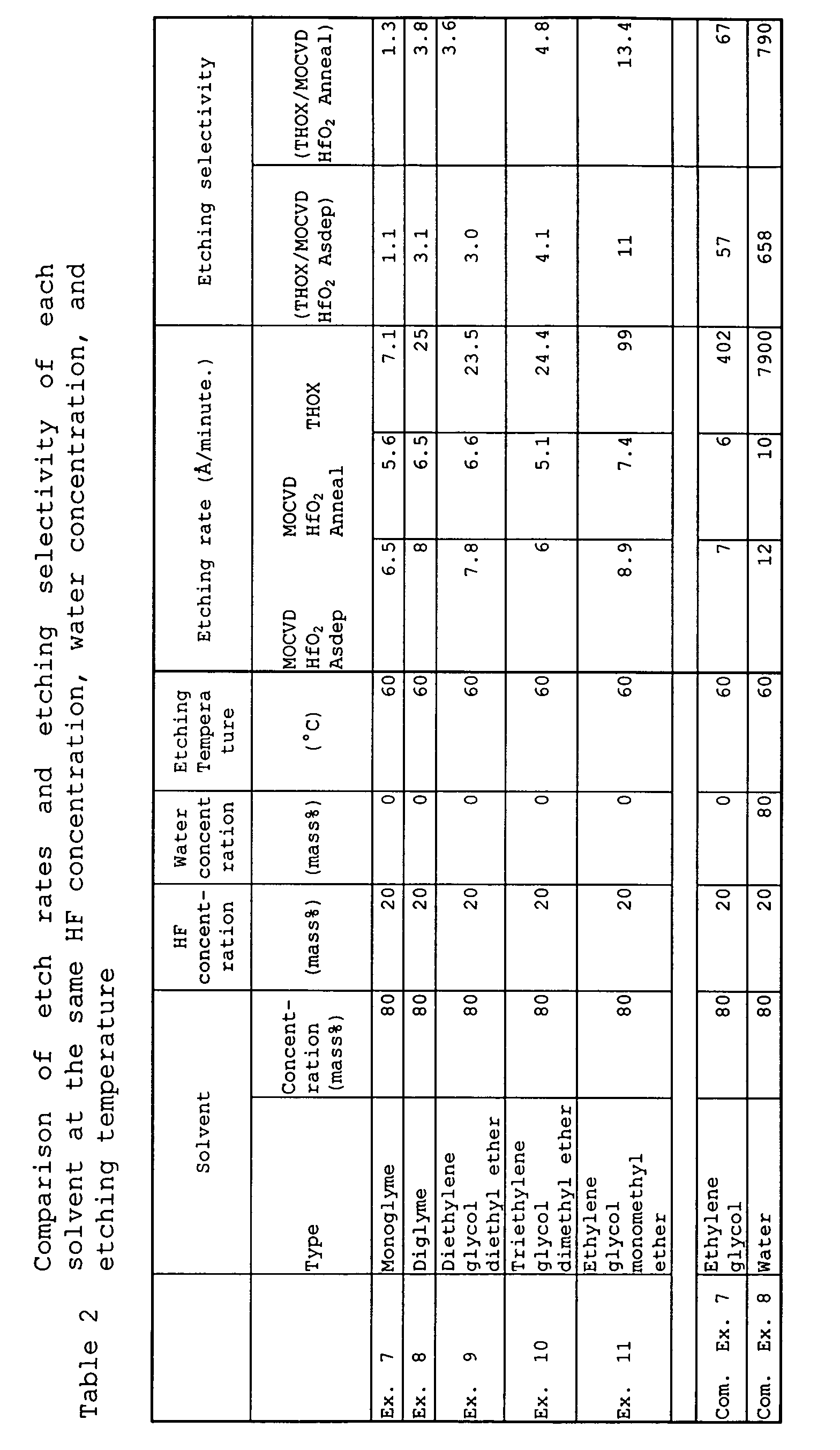
  • Table 2 shows the etch rates and etching selectivity of etching solution (Examples 7 to 11 and Comparative Examples 7 to 8) containing an ether compound solvent as set forth in Claim 9, using the same HF concentration and water concentration (0%) at the same etching temperature (60°C), for etching MOCVD HfO 2 Asdep, MOCVD HfO 2 Anneal, and thermal oxide film (THOX).
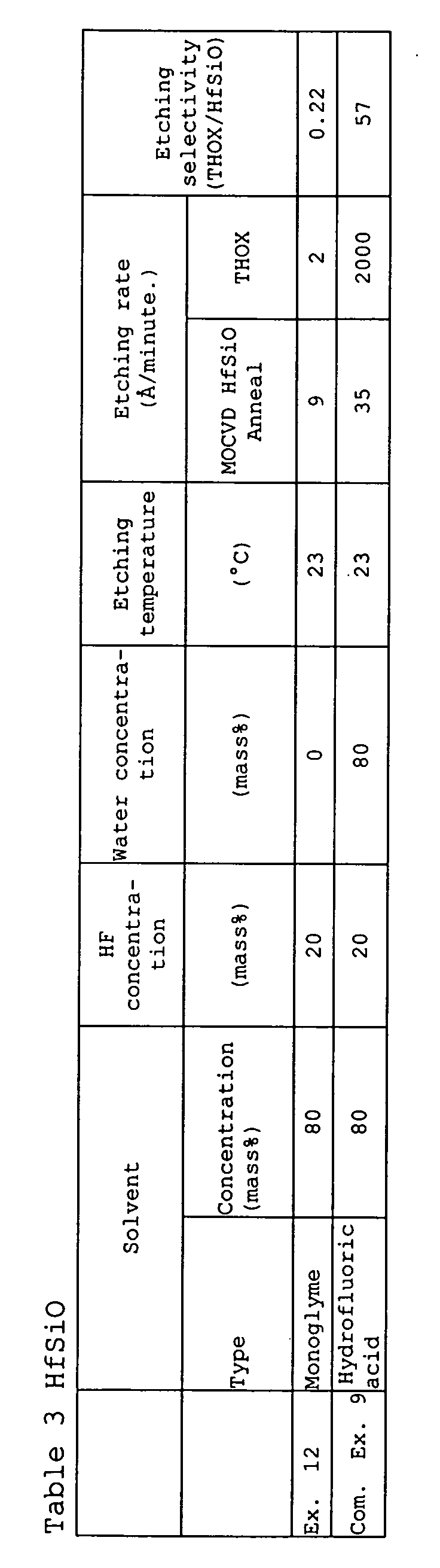
  • Tables 3 and 4 show the etch rates and etching selectivity of monoglyme and HF in an anhydrous hydrofluoric acid-containing etching solutions (Examples 12 and 13, and Comparative Examples 9 and 10) for MOCVD HfSiO Anneal film, MOCVD Al 2 O 3 Anneal film, and thermal oxide (THOX) film.

Landscapes

  • Chemical & Material Sciences (AREA)
  • Inorganic Chemistry (AREA)
  • Engineering & Computer Science (AREA)
  • Materials Engineering (AREA)
  • Organic Chemistry (AREA)
  • Weting (AREA)
  • Electrodes Of Semiconductors (AREA)
  • Insulated Gate Type Field-Effect Transistor (AREA)

Abstract

An etching solution having an etch rate of 2 ANGSTROM /minute or greater for a film having a relative dielectric constant of 8 or higher (a High-k film, and whose ratio of the etch rate of a thermal oxide (THOX) film to that of a High-k film is (ÄTHOX etch rateÜ/ÄHigh-k film etch rateÜ) is 50 or less. <IMAGE>

Description

TECHNICAL FIELD
The present invention relates to an etching solution, a method for producing an etched article and an etched article obtained by the method.
BACKGROUND OF THE INVENTION
In recent years, there has been an increased need for narrowing gate widths due to the miniaturization of semiconductor devices. According to a scaling law, this also requires the effective film thickness of a gate insulating film to be thin. However, if an SiO2 film, which is currently used as a gate insulating film in silicon devices, is further thinned, this renders a problem of increased current leakage and/or decreased reliability. To solve this problem, a method wherein a physical film thickness is increased by using a high-dielectric material (High-k material) for a gate insulating film has been proposed. Examples of such high-dielectric materials are hafnium oxide, zirconium oxide films, etc. These High-k films usually have extremely high etching resistivity. An etching solution that can etch a High-k film, if it etches too quickly a THOX, TEOS or the like Si oxide film that is formed on an Si substrate prior to the High-k film etching process, is undesirable, because the Si oxide film will be etched to such an extent that it cannot achieve its function as an Si oxide film. Therefore, there is a demand for an etching solution that can etch High-k films while its silicon oxide film etching speed is suppressed (for example, see Experimental observation of the thermal stability of High-k gate dielectric material on silicon, P. S. Lysaght et al., Journal of Non-Crystalline Solids, 303(2002) 54-63; Integration of High-k gate stack systems into planar CMOS process flows, H. R. Huff et al., IWGI 2001, Tokyo; Selective & Non-Selective Wet Etching, M. Itano et al., Wafer Clean & Surface Prep Workshop, International Sematech).
An object of the present invention is to provide an etching solution that can etch a High-k film but etch a silicon oxide film at a reduced speed.
BRIEF DESCRIPTION OF THE DRAWINGS
Fig. 1 schematically shows an example of an etched article of the present invention.
DISCLOSURE OF THE INVENTION
The present invention relates to the inventions described in the following items.
Item 1. An etching solution having an etch rate of 2 Å/minute or greater for a film having a relative dielectric constant of 8 or higher (a High-k film), and whose ratio of the etch rate for a thermal oxide (THOX) film to the etch rate for a High-k film ([THOX etch rate]/[High-k film etch rate]) is 50 or less.
Item 2. An etching solution according to Item 1, wherein the High-k film has a relative dielectric constant of 15 or greater.
Item 3. An etching solution according to Item 1, wherein the High-k film is a hafnium oxide film, a zirconium oxide film, or a lanthanum oxide film.
Item 4. An etching solution according to Item 1, wherein the High-k film comprises at least one member selected from the group consisting of hafnium silicate (HfSiOx), hafnium aluminate (HfAlO), HfSiON, HfAlON, ZrSiO, ZrAlO, ZrSiON, ZrAlON, alumina (Al2O3), HfON, ZrON and Pr2O3.
Item 5. An etching solution according to Item 1, wherein the etch rate for the thermal oxide (THOX) film is 100 Å/minute or less.
Item 6. An etching solution according to Item 1, which contains hydrogen fluoride (HF).
Item 7. An etching solution according to Item 1 wherein the hydrogen fluoride concentration is 3 mass% or greater.
Item 8. An etching solution according to Item 1, which contains hydrogen fluoride and an organic solvent comprising a heteroatom.
Item 9. An etching solution according to Item 8, wherein the organic solvent comprising a heteroatom is an ether compound, a ketone compound, or a sulfur-containing heterocyclic compound.
Item 10. An etching solution according to Item 9, wherein the organic solvent comprising a heteroatom is an ether compound.
Item 11. An etching solution according to Item 10, wherein the ether compound is at least one member selected from the group consisting of compounds represented by General Formula (1) R1-O-(CH2CH2-O)n-R2    wherein n is 1, 2, 3 or 4, R1 and R2 may be the same or different and each represents a hydrogen atom, a lower alkyl group or a lower alkyl carbonyl group, with the proviso that R1 and R2 are not both hydrogen atoms.
Item 12. An etching solution according to Item 10, wherein the ether compound has a relative dielectric constant of 30 or less.
Item 13. An etching solution according to Item 8, wherein the organic solvent comprising a heteroatom contains at least one carbonyl group in its molecular.
Item 14. An etching solution according to Item 8, wherein the organic solvent comprising a heteroatom has at least one hydroxy group in its molecular.
Item 15. An etching solution according to Item 10, wherein the ether compound is at least one member selected from the group consisting of tetrahydrofuran, tetrahydropyran, furan, furfural, γ-butyrolactone, monoglyme, diglyme, and dioxane.
Item 16. An etching solution according to Item 10, wherein the ether compound is at least one member selected from the group consisting of ethylene glycol methyl ethyl ether, ethylene glycol diethyl ether, diethylene glycol methyl ethyl ether, diethylene glycol diethyl ether, triethylene glycol dimethyl ether, triethylene glycol diethyl ether, triethylene glycol ethylmethyl ether, tetraethylene glycol dimethyl ether, tetraethylene glycol diethyl ether, and polyethylene glycol dimethyl ether.
Item 17. An etching solution according to Item 10, wherein the ether compound is at least one member selected from the group consisting of ethylene glycol monomethyl ether acetate, ethylene glycol monoethyl ether acetate, ethylene glycol monobutyl ether acetate, diethylene glycol monomethyl ether acetate, diethylene glycol monoethyl ether acetate, diethylene glycol monobutyl ether acetate, triethylene glycol monomethyl ether acetate and triethylene glycol monoethyl ether acetate.
Item 18. An etching solution according to Item 10, wherein the ether compound is at least one member selected from the group consisting of an ethylene glycol monomethyl ether, ethylene glycol monoethyl ether, ethylene glycol monopropyl ether, polyethylene glycol monomethyl ether, ethylene glycol monoisopropyl ether, ethylene glycol monobutyl ether, propylene glycol monomethyl ether, propylene glycol monopropyl ether and propylene glycol monobutyl ether.
Item 19. An etching solution according to Item 9, wherein the sulfur-containing heterocyclic compound is at least one member selected from the group consisting of sulfolane and propane sultone.
Item 20. An etching solution according to Item 1, which contains hydrogen fluoride (HF) and an organic solvent comprising a heteroatom, wherein the ratio of HF : heteroatom-comprising organic solvent : water = 3 mass% or greater : 50 to 97 mass% : 10 mass% or less.
Item 21. A method for producing an etched article using the etching solution of Item 1, the method comprising a step of etching an object to be etched having a silicon oxide film and a film having a relative dielectric constant of 8 or greater, and a gate electrode that is formed on the film having a relative dielectric constant of 8 or greater.
Item 22. An etched article obtained by the method of Item 21.
The etching solution of the present invention has a ratio of the etch rate of a thermal oxide (THOX) film relative to that of a film having a high relative dielectric constant (High-k film) ([THOX etch rate]/[High-k film etch rate]), i.e., etching selectivity, of 50 or less. According to a preferable embodiment of the present invention, the etching solution of the present invention has an etch rate for a High-k film of 2 Å/minute or greater, preferably about 5 Å/minute or greater, and more preferably about 10 to 30 Å/minute.
A film having a relative dielectric constant of about 8 or greater, preferably about 15 or greater, and more preferably about 20 to 40 is used as the film having a high relative dielectric constant (High-k film). The upper limit of the relative dielectric constant is about 50. Examples of materials for such High-k films are hafnium oxide, zirconium oxide, lanthanum oxide, hafnium silicates (HfSiOx), hafnium aluminates (HfAlOx), HfSiON, HfAlON, ZrSiO, ZrAlO, ZrSiON, ZrAlON, alumina (Al2O3), HfON, ZrON, Pr2O3, etc. The relative dielectric constant of each material is as follows: alumina = 8.5 to 10, aluminates (HfAlO, HfAlON, ZrAlO, ZrAlON) = 10 to 20, silicates (HfSiO, HfSiON, ZrSiO, ZrSiON) = 10 to 20, hafnium oxides = 24, and zirconium oxides = 11 to 20.
The etching solution of the present invention has a ratio of THOX etch rate to that of High-k film (THOX etch rate/High-k film etch rate) of 50 or less, preferably about 20 or less, more preferably about 10 or less, still more preferably about 5 or less, yet still more preferably about 1 or less, and particularly preferably about 1/10 or less.
It is preferable that the ratio of etch rates of High-k film to THOX be within the above mentioned ranges for the following reasons:
In a process for fabricating a semiconductor device, during a step of etching a High-k gate oxide film, an Si oxide film is formed on an Si substrate to separate each device in an IC by STI (Shallow Trench isolation) or like method, and on the gate oxide film, a thin interlayer of an Si oxide film is formed between a High-k oxide layer and an Si substrate (see Fig. 1). When a High-k film is overetched in the process of etching a High-k gate oxide film, and if a base film thereof, i.e., an Si oxide film, is etched, the capabilities of the film are adversely affected, and this causes problems. An ideal etching solution is one that does not etch Si oxide films but etches only High-k films. However, unless the High-k films have an extremely high uniformity in the thickness and etch rate, and just etching is conducted, these Si oxide films will not be etched, and therefore, no problems arise. When the etching selectivity is within the above range, it is possible to not etch the Si oxide film by controlling the etching time, etc., and is therefore preferable. If the etching solution has an etching selectivity within the above range, even when a High-k film is overetched, it is possible to control the degree of overetching so that is does not adversely affect the abilities of the Si oxide film. Because the Si oxide film of the interlayer is etched from the side, it takes a long time to be etched, and therefore if etching selectivity is within the above range, it is possible to control so that the Si oxide film is etched to an extent that does not cause any problems.
The etching solution of the present invention has an etch rate for a High-k film about 2 Å/minute or greater, preferably about 5 Å/minute or greater, and more preferably about 10 Å/minute or greater.
From the viewpoint of throughput in the wet etching process of a High-k gate oxide film, it is preferable that the etch rate of High-k film be about 2 Å/minute or greater.
All that is necessary for the etching solution of the invention is that the requirements, i.e., its High-k film etch rate is 2 Å/minute or greater and the ratio of the High-k film etch rate to thermal oxide (THOX) film etch rate is 50 or less, are met at a temperature within the range that the etching solution can etch. In other words, it is necessary that the etching solution of the present invention meets the two requirements described above at a desired temperature. Preferably, the etching solution meets the two requirements at any one temperature not less than 20°C, more preferably in the range from 20°C to the boiling point of the solvent, more preferably about 20 to 90°C, still more preferably about 20 to 60°C, and still further more preferably about 20 to 30°C.
The etching solution of the present invention has a THOX etch rate of about 100 Å/minute or less, preferably about 50 Å/minute or less, more preferably about 20 Å/minute or less, and particularly preferably about 1 Å/minute or less. The etching solution temperature depends on the type of the etching solution, and may be any temperature as long as the etching solution can etch and meet the above requirements, preferably any temperature 20°C or greater, and more preferably any temperature within the range from 20°C to not more than the boiling point of the solvent, more preferably any temperature within the range from 20 to 60°C, and still more preferably from 20 to 30°C.
If an etching solution can etch a thermal oxide (THOX) film in such a manner to have an etch rate ratio relative to High-k film in the range as described above, the etching solution can also etch TEOS or other like silicon oxide films at a similar ratio.
The etch rate of the etching solution of the present invention can be obtained by dividing the difference in thickness of the film (High-k film, THOX, TEOS and like silicon oxide films, etc.) before and after etching using the etching solution of the present invention by the etching time.
Examples of etching solutions of the present invention are those containing hydrogen fluoride (HF), preferably those containing hydrogen fluoride and an organic solvent comprising a heteroatom.
The HF content is preferably about 3 mass% or more and more preferably about 10 mass% or more. The upper limit of the HF content is not particularly limited; however, it is preferably about 50 mass%, more preferably about 35 mass%, and still more preferably about 25 mass%. Usually, when the HF content is great, the High-k film etch rate tends to be high. In contrast, when the HF content is small, the ratio of the etch rates of THOX to High-k film ([THOX etch rate]/[High-k film etch rate]) tends to be small. Therefore, the HF concentration can be suitably selected depending on the desired High-k film etch rate and the desired ratio of etch rates of THOX to High-k films.
Hydrofluoric acid (cone.; 50 mass% solution) is usually used as HF; however, when an etching solution without water is preferable, 100% HF may also be used.
A method for preparing an etching solution containing hydrogen fluoride (HF) is that, when hydrofluoric acid (conc.) is used, a hydrofluoric acid (conc.) solution is added to an organic solvent comprising a heteroatom or heteroatoms. When 100% HF is used, the 100% HF is mixed with a solution or the 100% HF is diluted. In this case, attention has to be paid to the heat generated during dilution.
Preferable examples of organic solvents comprising a heteroatom or heteroatoms are ether compounds, ketone compounds, sulfur-containing compounds, etc.
Among these, ether compounds are preferable.
Ether compounds may be open-chain compounds or cyclic compounds, and preferable examples thereof are those represented by the following General Formula (1). R1-O-(CH2CH2-O)n-R2    wherein n is 1, 2, 3 or 4, R1 and R2 may be the same or different and each represents a hydrogen atom, a lower alkyl group or a lower alkyl carbonyl group, with the proviso that R1 and R2 are not both hydrogen atoms at the same time.
As a lower alkyl group, an alkyl group having about 1 to 3 carbon atoms is preferably used, examples thereof include the methyl, ethyl, n-propyl, and isopropyl groups.
Preferable examples of lower alkyl groups of a lower alkyl carbonyl group are C1-C3 alkyl groups (methyl, ethyl, n-propyl, and isopropyl), and examples of lower alkyl carbonyl groups are acetyl, propionyl, butyryl and isobutyryl.
Examples of preferable compounds represented by General Formula (1) are monoglyme (n = 1); diglyme and diethylene glycol diethyl ether (n = 2); triethylene glycol dimethyl ether (n = 3); and tetraethylene glycol dimethyl ether (n = 4).
Examples of other ether compounds are tetrahydrofuran, tetrahydropyran, furan, furfural, γ-butyrolactone, dioxane, etc.
Among these ether compounds, monoglyme, diglyme, tetrahydrofuran, diethylene glycol diethyl ether, triethylene glycol dimethyl ether, tetraethylene glycol dimethyl ether, dioxane, and γ-butyrolactone are preferable, and monoglyme is particularly preferable.
As ether compounds, those having a relative dielectric constant of 30 or less can be preferably used. Examples of ether compounds having a relative dielectric constant of 30 or less include monoglyme, diglyme, tetrahydrofuran, dioxane, γ-butyrolactone, etc.
Examples of ketone compounds are γ-butyrolactone and like cyclic compounds.
Examples of sulfur-containing compounds are sulfolane, propane sultone and like cyclic compounds.
The etching solution of the present invention may contain water. When it contains water, the content of water is 10 mass% or less, preferably 5 mass% or less, and more preferably about 3 mass%. However, as the etching solution of the present invention, those without water are preferable.
A preferable example of an etching solution of the present invention is:
  • HF : organic solvent comprising a heteroatom (preferably, ether compound) : water = 3 mass% or greater : 50 to 97 mass% : 10 mass% or less. More specifically, the following etching solutions are exemplified:
  • HF : monoglyme : water = 3 to 50 mass% : 50 to 97 mass% : 0 to 10 mass%
  • HF : diglyme : water = 3 to 50 mass% : 50 to 97 mass% : 0 to 10 mass%
  • HF : dioxane : water = 3 to 50 mass% : 50 to 97 mass% : 0 to 10 mass%
  • HF : tetrahydrofuran : water = 3 to 50 mass% : 50 to 97 mass% : 0 to 10 mass%
  • HF : diethylene glycol diethyl ether : water = 1 to 20 mass% : 70 to 99 mass% : 0 to 10 mass%
  • HF : triethylene glycol dimethyl ether : water = 1 to 20 mass% : 70 to 99 mass% : 0 to 10 mass%
  • HF : tetraethylene glycol dimethyl ether : water = 1 to 20 mass% : 70 to 99 mass% : 0 to 10 mass%
The etching solution of the present invention can be suitably used for etching an object that has a High-k film, and a THOX, TEOS and/or like silicon oxide film on the surface of a silicon substrate.
The etching solution can be used in a process for fabricating a semiconductor. The fabrication process comprises, for example, the steps of: forming an isolation region on the silicon substrate by embedding THOX, TEOS or like silicon oxide in a trench to form a High-k film; forming a gate electrode; and forming a gate insulating film by etching the High-k film using, for example, the gate electrode as a mask.
Before conducting etching using the etching solution of the present invention, dry etching may be conducted in such a manner that some portion of the High-k film remains unetched. In other words, when a High-k film is etched by two-step etching, sometimes the top portion of the High-k film is etched by dry etching and wet etching is conducted to remove the rest of the High-k film. The etching solution of the present invention can be used in the wet etching.
In the etching method of the present invention, the etching solution temperature is not limited as long as the High-k film and the THOX can be etched at desired etch rates with a desired etching selectivity, and it can be suitably selected depending on the type of High-k film and etching solution, and other conditions. For example, in the case of an etching solution containing hydrogen fluoride, when the hydrogen fluoride concentration is high, the requirement "High-k film etch rate of 2 Å/minute or greater" can be met at a relatively low temperature; however, when the hydrogen fluoride concentration is low, it is necessary to conduct etching at a relatively high temperature to meet this requirement.
Therefore, the temperature may be suitably selected so as to meet the requirements of the present invention depending on the kind of the etching solution and content of each component of the etching solution. The etching solution temperature is usually about 20 to 90°C and preferably about 20 to 60°C.
The etching treatment can be conducted by following a conventional method, for example, dipping an object to be etched in an etching solution. The duration of dipping is not limited as long as it can etch the High-k film and the THOX to a desired thickness at a desired etch rate and etching selectivity. Therefore the dipping time can be suitably selected depending on the types of High-k film and etching solution, solution temperature of the etching solution, etc. The dipping time is usually about 1 to 30 minutes and preferably about 1 to 10 minutes.
The semiconductor substrate etched using the etching solution of the present invention can be fabricated into various types of semiconductor devices by employing conventional methods (for example, methods disclosed in Atlas of IC Technologies: An Introduction to VLSI Processes by W. Maly, 1987 by The Benjamin/Cummings Publishing Company Inc.).
The present invention provides an etching solution that can etch a High-k film, while etching a silicon oxide film at a suppressed etch rate.
BEST MODE FOR CARRYING OUT THE INVENTION
Examples of the present invention are described below; however the scope of the present invention is not limited to or by these examples.
Examples 1 to 13 and Comparative Examples 1 to 10
Etching solutions which contain HF and solvent in the ratio as shown in Tables 1, 2, 3 and 4 were prepared. Etch rates and etching selectivity of each solution were obtained in respect to each test substrate comprising, on a silicon substrate, a hafnium oxide film (MOCVD HfO2 Asdep) formed by MOCVD, a film formed by annealing the hafnium oxide film (MOCVD HfO2 Anneal), a hafnium silicate film (HfSiO) formed by MOCVD and annealing, alumina (Al2O3) formed by MOCVD and annealing, or thermal oxide (THOX) film.
The etch rate was determined by measuring the thicknesses of the films before and after etching and dividing the thickness diference by the etching time.
The thicknesses of the films were measured using an Auto EL-III ellipsometer manufactured by Rudolf Research.
Etching was conducted by dipping each test substrate into an etching solution for 10 minutes.
Table 1 shows the etch rates and etching selectivity of each etching solution (Examples 1 to 6 and Comparative Examples 1 to 6) for a MOCVD HfO2 Asdep, MOCVD HfO2 Anneal, and thermal oxide (THOX) film at an etching temperature of 50°C.
Table 2 shows the etch rates and etching selectivity of etching solution (Examples 7 to 11 and Comparative Examples 7 to 8) containing an ether compound solvent as set forth in Claim 9, using the same HF concentration and water concentration (0%) at the same etching temperature (60°C), for etching MOCVD HfO2Asdep, MOCVD HfO2 Anneal, and thermal oxide film (THOX).
Tables 3 and 4 show the etch rates and etching selectivity of monoglyme and HF in an anhydrous hydrofluoric acid-containing etching solutions (Examples 12 and 13, and Comparative Examples 9 and 10) for MOCVD HfSiO Anneal film, MOCVD Al2O3 Anneal film, and thermal oxide (THOX) film.
Figure 00140001
Figure 00150001
Figure 00160001
Figure 00170001

Claims (22)

  1. An etching solution having an etch rate of 2 Å/minute or greater for a film having a relative dielectric constant of 8 or higher (a High-k film), and whose ratio of the etch rate for a thermal oxide (THOX) film to the etch rate for a High-k film ([THOX etch rate]/[High-k film etch rate]) is 50 or less.
  2. An etching solution according to Claim 1, wherein the High-k film has a relative dielectric constant of 15 or greater.
  3. An etching solution according to Claim 1, wherein the High-k film is a hafnium oxide film, a zirconium oxide film, or a lanthanum oxide film.
  4. An etching solution according to Claim 1, wherein the High-k film comprises at least one member selected from the group consisting of hafnium silicate (HfSiOx), hafnium aluminate (HfAlO), HfSiON, HfAlON, ZrSiO, ZrAlO, ZrSiON, ZrAlON, alumina (Al2O3), HfON, ZrON and Pr2O3.
  5. An etching solution according to Claim 1, wherein the etch rate for the thermal oxide (THOX) film is 100 Å/minute or less.
  6. An etching solution according to Claim 1, which contains hydrogen fluoride (HF).
  7. An etching solution according to Claim 1, wherein the hydrogen fluoride concentration is 3 mass% or greater.
  8. An etching solution according to Claim 1, which contains hydrogen fluoride and an organic solvent comprising a heteroatom.
  9. An etching solution according to Claim 8, wherein the organic solvent comprising a heteroatom is an ether compound, a ketone compound, or a sulfur-containing heterocyclic compound.
  10. An etching solution according to Claim 9, wherein the organic solvent comprising a heteroatom is an ether compound.
  11. An etching solution according to Claim 10, wherein the ether compound is at least one member selected from the group consisting of compounds represented by General Formula (1) R1-O-(CH2CH2-O)n-R2    wherein n is 1, 2, 3 or 4, R1 and R2 may be the same or different and each represents a hydrogen atom, a lower alkyl group or a lower alkyl carbonyl group, with the proviso that R1 and R2 are not both hydrogen atoms.
  12. An etching solution according to Claim 10, wherein the ether compound has a relative dielectric constant of 30 or less.
  13. An etching solution according to Claim 8, wherein the organic solvent comprising a heteroatom contains at least one carbonyl group in its molecular.
  14. An etching solution according to Claim 8, wherein the organic solvent comprising a heteroatom has at least one hydroxy group in its molecular.
  15. An etching solution according to Claim 10, wherein the ether compound is at least one member selected from the group consisting of tetrahydrofuran, tetrahydropyran, furan, furfural, γ-butyrolactone, monoglyme, diglyme, and dioxane.
  16. An etching solution according to Claim 10, wherein the ether compound is at least one member selected from the group consisting of ethylene glycol methyl ethyl ether, ethylene glycol diethyl ether, diethylene glycol methyl ethyl ether, diethylene glycol diethyl ether, triethylene glycol dimethyl ether, triethylene glycol diethyl ether, triethylene glycol ethylmethyl ether, tetraethylene glycol dimethyl ether, tetraethylene glycol diethyl ether, and polyethylene glycol dimethyl ether.
  17. An etching solution according to Claim 10, wherein the ether compound is at least one member selected from the group consisting of ethylene glycol monomethyl ether acetate, ethylene glycol monoethyl ether acetate, ethylene glycol monobutyl ether acetate, diethylene glycol monomethyl ether acetate, diethylene glycol monoethyl ether acetate, diethylene glycol monobutyl ether acetate, triethylene glycol monomethyl ether acetate and triethylene glycol monoethyl ether acetate.
  18. An etching solution according to Claim 10, wherein the ether compound is at least one member selected from the group consisting of an ethylene glycol monomethyl ether, ethylene glycol monoethyl ether, ethylene glycol monopropyl ether, polyethylene glycol monomethyl ether, ethylene glycol monoisopropyl ether, ethylene glycol monobutyl ether, propylene glycol monomethyl ether, propylene glycol monopropyl ether and propylene glycol monobutyl ether.
  19. An etching solution according to Claim 9, wherein the sulfur-containing heterocyclic compound is at least one member selected from the group consisting of sulfolane and propane sultone.
  20. An etching solution according to Claim 1, which contains hydrogen fluoride (HF) and an organic solvent comprising a heteroatom, wherein the ratio of HF : heteroatom-comprising organic solvent : water = 3 mass% or greater : 50 to 97 mass% : 10 mass% or less.
  21. A method for producing an etched article using the etching solution of Claim 1, the method comprising a step of etching an object to be etched having a silicon oxide film and a film having a relative dielectric constant of 8 or greater, and a gate electrode that is formed on the film having a relative dielectric constant of 8 or greater.
  22. An etched article obtained by the method of Claim 21.
EP03795208A 2002-09-13 2003-08-04 ATTACK AGENT AND ATTACK METHOD Withdrawn EP1538664A4 (en)

Applications Claiming Priority (5)

Application Number Priority Date Filing Date Title
JP2002269291 2002-09-13
JP2002346823 2002-11-29
PCT/JP2003/009848 WO2004025718A1 (en) 2002-09-13 2003-08-04 Etchant and etching method

Publications (2)

Publication Number Publication Date
EP1538664A1 true EP1538664A1 (en) 2005-06-08
EP1538664A4 EP1538664A4 (en) 2007-04-04

Family

ID=31996189

Family Applications (1)

Application Number Title Priority Date Filing Date
EP03795208A Withdrawn EP1538664A4 (en) 2002-09-13 2003-08-04 ATTACK AGENT AND ATTACK METHOD

Country Status (8)

Country Link
US (1) US20060011584A1 (en)
EP (1) EP1538664A4 (en)
JP (1) JP4221601B2 (en)
KR (1) KR100742069B1 (en)
CN (1) CN1682355A (en)
AU (1) AU2003252362A1 (en)
TW (1) TWI282814B (en)
WO (1) WO2004025718A1 (en)

Cited By (1)

* Cited by examiner, † Cited by third party
Publication number Priority date Publication date Assignee Title
EP1828070A4 (en) * 2004-09-10 2008-11-05 Honeywell Int Inc CHEMICAL ATTACK AGENT OF CONSTANT SELECTIVE MATERIAL WITH HIGH DIELECTRIC

Families Citing this family (19)

* Cited by examiner, † Cited by third party
Publication number Priority date Publication date Assignee Title
JP4229762B2 (en) 2003-06-06 2009-02-25 Necエレクトロニクス株式会社 Manufacturing method of semiconductor device
JP2005079311A (en) * 2003-08-29 2005-03-24 Semiconductor Leading Edge Technologies Inc Method of manufacturing semiconductor device
WO2006101458A1 (en) * 2005-03-22 2006-09-28 National University Of Singapore Method for patterning ferrelectric/piezoelectric films
KR100927080B1 (en) * 2005-05-25 2009-11-13 다이킨 고교 가부시키가이샤 Etchant for substrates having bpsg and sod layers
US20070012662A1 (en) * 2005-07-18 2007-01-18 Audrey Dupont Solution for wet treatment of hafnium containing materials, use of the solution and a wet treatment process
KR100780638B1 (en) * 2006-05-31 2007-11-29 주식회사 하이닉스반도체 Flash memory device and manufacturing method thereof
EP2268765A4 (en) * 2008-03-07 2011-10-26 Advanced Tech Materials MOISTURE CLEANING COMPOSITION BY ATTACKING NON-SELECTIVE OXIDE AND METHOD OF USE
JP5127694B2 (en) * 2008-12-26 2013-01-23 パナソニック株式会社 Semiconductor device and manufacturing method thereof
JP5535583B2 (en) 2009-05-25 2014-07-02 AzエレクトロニックマテリアルズIp株式会社 Method for forming trench isolation structure
JP5592083B2 (en) * 2009-06-12 2014-09-17 アイメック Substrate processing method and semiconductor device manufacturing method using the same
CN102460662B (en) * 2009-06-25 2014-09-10 朗姆研究公司 Method for processing semiconductor wafers
US20130334603A1 (en) * 2012-06-18 2013-12-19 International Business Machines Corporation Isolation structure for semiconductor devices
CN103204709B (en) * 2013-03-01 2014-06-18 中国科学院长春光学精密机械与物理研究所 Method for removing silicon thick-film on silicon carbide substrate
WO2014178426A1 (en) * 2013-05-02 2014-11-06 富士フイルム株式会社 Etching method, etching liquid and etching liquid kit to be used in said method, and semiconductor substrate product manufacturing method
TWI635160B (en) * 2014-03-07 2018-09-11 東友精細化工有限公司 Texture etching solution composition and texture etching method of crystalline silicon wafers
KR101863536B1 (en) * 2014-03-07 2018-06-01 동우 화인켐 주식회사 Texture etching solution composition and texture etching method of crystalline silicon wafers
KR101892624B1 (en) 2014-03-17 2018-08-28 동우 화인켐 주식회사 Texture etching solution composition and texture etching method of crystalline silicon wafers
TWI895691B (en) * 2023-02-14 2025-09-01 關東鑫林科技股份有限公司 Etching solution composition and etching method using the same
CN119552660A (en) * 2024-11-22 2025-03-04 湖北兴福电子材料股份有限公司 A kind of hafnium dioxide etching solution and preparation method thereof

Family Cites Families (30)

* Cited by examiner, † Cited by third party
Publication number Priority date Publication date Assignee Title
US3438799A (en) * 1965-06-22 1969-04-15 Chem Eng Ltd Method for the surface treatment of metal articles
JPS5349508A (en) * 1976-10-18 1978-05-06 Fuji Photo Film Co Ltd Liquid for weakening screen dot
JPS5530826A (en) * 1978-08-24 1980-03-04 Nec Kyushu Ltd Method of manufacturing semiconductor device
US4469525A (en) * 1983-01-19 1984-09-04 Tennant Company Membrane remover/etchant
US5120605A (en) * 1988-09-23 1992-06-09 Zuel Company, Inc. Anti-reflective glass surface
JP3120566B2 (en) * 1992-05-12 2000-12-25 株式会社デンソー Method for forming bump electrode in semiconductor device
JP3563809B2 (en) * 1995-02-14 2004-09-08 大日本印刷株式会社 Pattern formation method
TW434196B (en) * 1997-06-25 2001-05-16 Ibm Selective etching of silicate
US5965465A (en) * 1997-09-18 1999-10-12 International Business Machines Corporation Etching of silicon nitride
JP4044215B2 (en) * 1998-02-25 2008-02-06 花王株式会社 Release agent composition
US6200891B1 (en) * 1998-08-13 2001-03-13 International Business Machines Corporation Removal of dielectric oxides
JP2000164586A (en) * 1998-11-24 2000-06-16 Daikin Ind Ltd Etching liquid
DE19914243A1 (en) * 1999-03-29 2000-10-05 Riedel De Haen Gmbh Process for the preparation of high-purity solutions using gaseous hydrogen fluoride
JP4516176B2 (en) * 1999-04-20 2010-08-04 関東化学株式会社 Substrate cleaning solution for electronic materials
JP5156155B2 (en) * 1999-10-13 2013-03-06 アプライド マテリアルズ インコーポレイテッド Method for manufacturing a semiconductor integrated circuit
WO2001057921A1 (en) * 2000-02-04 2001-08-09 Motorola Inc. Etching solution and method
JP2001332547A (en) * 2000-03-17 2001-11-30 Toshiba Corp Semiconductor device and method of manufacturing semiconductor device
AU4251001A (en) * 2000-04-28 2001-11-12 Merck Patent Gmbh Etching pastes for inorganic surfaces
US6300202B1 (en) * 2000-05-18 2001-10-09 Motorola Inc. Selective removal of a metal oxide dielectric
EP1360077A4 (en) * 2000-07-10 2009-06-24 Ekc Technology Inc COMPOSITIONS FOR REMOVING ORGANIC RESIDUES AND PLASMA ETCHING FOR SEMICONDUCTOR DEVICES
JP3727299B2 (en) * 2001-12-04 2005-12-14 松下電器産業株式会社 Manufacturing method of semiconductor device
US6667246B2 (en) * 2001-12-04 2003-12-23 Matsushita Electric Industrial Co., Ltd. Wet-etching method and method for manufacturing semiconductor device
JP3751255B2 (en) * 2002-03-04 2006-03-01 岸本産業株式会社 Insulating film etchant
US6941956B2 (en) * 2002-03-18 2005-09-13 Dainippon Screen Mfg. Co., Ltd. Substrate treating method and apparatus
JP3773458B2 (en) * 2002-03-18 2006-05-10 大日本スクリーン製造株式会社 Substrate processing method and apparatus
JP2003273068A (en) * 2002-03-19 2003-09-26 Dainippon Screen Mfg Co Ltd Wafer processing method
JP2003332297A (en) * 2002-05-10 2003-11-21 Daikin Ind Ltd Etching solution and etching method
US6835667B2 (en) * 2002-06-14 2004-12-28 Fsi International, Inc. Method for etching high-k films in solutions comprising dilute fluoride species
JP4443864B2 (en) * 2002-07-12 2010-03-31 株式会社ルネサステクノロジ Cleaning solution for removing resist or etching residue and method for manufacturing semiconductor device
JP2006098421A (en) * 2003-06-10 2006-04-13 Daikin Ind Ltd Removal liquid and removal method for antireflection film containing silicon and filling material

Cited By (1)

* Cited by examiner, † Cited by third party
Publication number Priority date Publication date Assignee Title
EP1828070A4 (en) * 2004-09-10 2008-11-05 Honeywell Int Inc CHEMICAL ATTACK AGENT OF CONSTANT SELECTIVE MATERIAL WITH HIGH DIELECTRIC

Also Published As

Publication number Publication date
WO2004025718A1 (en) 2004-03-25
CN1682355A (en) 2005-10-12
JP4221601B2 (en) 2009-02-12
TW200404091A (en) 2004-03-16
US20060011584A1 (en) 2006-01-19
EP1538664A4 (en) 2007-04-04
AU2003252362A1 (en) 2004-04-30
TWI282814B (en) 2007-06-21
KR100742069B1 (en) 2007-07-23
KR20050043947A (en) 2005-05-11
JPWO2004025718A1 (en) 2006-01-12

Similar Documents

Publication Publication Date Title
EP1538664A1 (en) Etchant and etching method
US10593538B2 (en) Surface treatment methods and compositions therefor
JP2009200506A (en) Etching agent composition for thin film having high permittivity
WO2010086745A1 (en) Method of etching lanthanum-containing oxide layers
US12104108B2 (en) Etching compositions
JP2003332297A (en) Etching solution and etching method
EP4017937A2 (en) Improved formulations for high selective silicon nitride etch
US12448568B2 (en) Etching compositions
KR101797162B1 (en) Silicon etching fluid and method for producing transistor using same
US20080110748A1 (en) Selective High Dielectric Constant Material Etchant
KR20150053212A (en) Composition for etching, and method for preparing semiconductor device using the same
JP2004311993A (en) High dielectric constant thin film etching composition
KR20100125464A (en) Film forming method and semiconductor device manufacturing method
JP2007150118A (en) Microfabrication processing agent and microfabrication processing method using same
TWI856294B (en) Composition of etchant, method for forming semiconductor device using the same, and semiconductor device
KR102443313B1 (en) Insulation layer etchant composition comprising the silane compound and method of forming pattern using the same
CN119979170B (en) Composition for microelectronic device selective removal of silicon germanium from silicon germanium/silicon stack
WO2001057921A1 (en) Etching solution and method
KR20220081169A (en) Etchant composition for etching silicon and method of manufacturing semiconductor device using the same
KR20210048306A (en) An etchant composition, a pattern formation method and a manufacturing method of array substrate using the etchant composition, and an array substrate manufactured therefrom
KR20200009988A (en) Insulation layer etchant composition and method of forming pattern using the same

Legal Events

Date Code Title Description
PUAI Public reference made under article 153(3) epc to a published international application that has entered the european phase

Free format text: ORIGINAL CODE: 0009012

17P Request for examination filed

Effective date: 20050316

AK Designated contracting states

Kind code of ref document: A1

Designated state(s): AT BE BG CH CY CZ DE DK EE ES FI FR GB GR HU IE IT LI LU MC NL PT RO SE SI SK TR

AX Request for extension of the european patent

Extension state: AL LT LV MK

DAX Request for extension of the european patent (deleted)
A4 Supplementary search report drawn up and despatched

Effective date: 20070307

RIC1 Information provided on ipc code assigned before grant

Ipc: H01L 21/311 20060101AFI20070301BHEP

17Q First examination report despatched

Effective date: 20080521

STAA Information on the status of an ep patent application or granted ep patent

Free format text: STATUS: THE APPLICATION HAS BEEN WITHDRAWN

18W Application withdrawn

Effective date: 20090327