BACKGROUND OF THE INVENTION
Field of the Invention
This invention relates to a method of and apparatus for reading
a radiation image where an image signal is obtained by integrating
by integrating amplifier charge signals output from a radiation image
sensor which stores a radiation image upon exposure to radiation
bearing thereon the radiation image and outputs charge signals
according to the stored radiation image upon exposure to reading
light.
Description of the Related Art
Various radiation image sensors on which a radiation image
of an object is recorded upon exposure to radiation passing through
the object and which outputs charge signals representing the recorded
radiation image have been proposed and put into practice.
As the radiation image sensor, there has been known those
employing semiconductor material which generates electric charges
upon exposure to radiation. As such radiation image sensors, there
have been proposed those of so-called an optical-reading system.
As the radiation image sensor of the optical-reading system,
a radiation image sensor comprising a first electrode layer permeable
to radiation, a recording photoconductive layer which generates
electric charges upon exposure to radiation, a charge transfer layer
which behaves like a substantially insulating material to the
electric charge in the same polarity as a latent image and behaves
like a substantially conductive material to the electric charge in
the polarity opposite to that of the latent image, a reading
photoconductive layer which generates electric charges upon exposure
to reading light, and a second electrode layer in which a plurality
of linear electrodes permeable to the reading light are arranged
in parallel to each other, the layers being superposed one on another
in this order, is proposed in U.S. Patent No. 6,770,901.
In the radiation image sensor, radiation is projected onto
the radiation image sensor from the first electrode layer side and
electric charges generated in the recording photoconductive layer
are stored on the interface between the recording photoconductive
layer and the charge transfer layer, thereby recording a radiation
image. When a linear reading light beam scans the radiation image
sensor in the longitudinal direction of the linear electrodes,
electric charges are generated in the reading photoconductive layer
and the electric charges are combined with the stored electric
charges and flow into the linear electrodes. The charge signals
flowing into the linear electrodes are integrated by integrating
amplifiers (so-called charge amplifiers) connected to the linear
electrodes, whereby an image signal is obtained and the radiation
image is read out.
Figure 9 shows a timing chart representing the relation
between the reading light beam projecting time and the integrating
time of the integrating amplifiers when the radiation image is read
out as well as the amplitude of the signal current output from the
linear electrodes of the radiation image sensor and the amplitude
of the output voltage of the integrating amplifiers.upon exposure
to the reading light beam. It is assumed that a radiation image has
been recorded on the radiation image sensor in the distribution shown
in Figure 9, that is, linear images extending in the same direction
as the reading light source are recorded in parallel at predetermined
intervals in the scanning direction of the reading light source,
i.e., in the direction of arrow X in Figure 9.
As shown in Figure 9, conventionally the recording light beam
is projected onto the radiation image sensor by continuously moving
the reading light source in the longitudinal direction of the linear
electrodes, and the image signal components (making up the image
signal) are obtained for each integrating time by turning on and
off the reset switches for the integrating amplifiers in response
to the movement of the reading light source.
However, projection of the reading light beam is
disadvantageous in that since the radiation image sensor is slow
in response speed to the reading light, for example, the signal
current output from the radiation image sensor in response to
projection of the reading light beam for integrating time S1 can
be continuously output from the radiation image sensor even in the
next integrating time S2 as shown in Figure 9 and accordingly, an
output voltage is output from the integrating amplifier as an image
signal component also in the integrating time S2 when the signal
current is to be 0 (the hatched portion in Figure 9), which forms
noise and deteriorates the image quality such as the sharpness of
the read radiation image.
Further, it has been proposed to use as the reading light source
a pulsed light source in place of the light source which continuously
emits the reading light, that is, to intermittently project the
recording light beam for integrating times. However, even in this
system, it is preferred that the reading light projecting time be
as long as possible and a method of ensuring a sufficient reading
light projecting time and at the same time avoiding generation of
the noise due to delay in response of the radiation image sensor
to the reading light has not been found.
There has been known so-called correlation double sampling
as a method of obtaining an image signal by the use of an integrating
amplifier. In the correlation double sampling, an image signal is
obtained on the basis of the difference between the output of the
integrating amplifier just after the initiation of the integration
and just before the termination of the integration. Accordingly,
if the reading light is projected onto the radiation image sensor
upon sampling of the output of the integrating amplifier just after
the initiation of the integration, the signal current output from
the radiation image sensor in response to projection of the reading
light creates an offset voltage and deteriorates the S/N of the read
radiation image.
SUMMARY OF THE INVENTION
In view of the foregoing observations and description, the
primary object of the present invention is to provide a method of
and apparatus for reading out a radiation image which can prevent
deterioration of the image quality such as sharpness of the read-out
image by ensuring a sufficient reading light projecting time and
at the same time avoiding generation of the noise due to delay in
response of the radiation image sensor to the reading light in a
method of and apparatus for reading a radiation image where an image
signal is obtained by integrating by integrating amplifier charge
signals output from a radiation image sensor which stores a radiation
image upon exposure to radiation bearing thereon the radiation image.
Another object of the present invention is to provide a method
of and apparatus for reading out a radiation image which can prevent
generation of the offset voltage as described above and deterioration
of the S/N of the read radiation image when the image signal is
obtained through the above correlation double sampling.
In accordance with an aspect of the present invention, there
is provided a method of reading out a radiation image comprising
the steps of
causing a linear reading light beam to scan a radiation image
sensor, on which a radiation image is recorded upon exposure to
radiation bearing thereon the radiation image and which has a
plurality of parallel linear electrodes to output charge signals
according to the radiation image when longitudinally scanned by a
linear reading light beam extending in a direction perpendicular
to the longitudinal direction of the linear electrodes, in the
longitudinal direction of its linear electrodes, and obtaining an
image signal by integrating charge signals, output by the respective
linear electrodes in response to the scan of the reading light beam,
for each integrating time, wherein the improvement comprises that
a pulsed light beam which is proj ected onto the radiation image
sensor for a predetermined time in each of the integrating times
is employed as the reading light beam, and
projection of the pulsed light beam is controlled so that the
center of the time for which the pulsed light beam is projected onto
the radiation image sensor is earlier than the center of the
integrating time.
In accordance with another aspect of the present invention,
there is provided an apparatus for reading out a radiation image
comprising
a reading light source portion which causes a linear reading
light beam to scan a radiation image sensor, on which a radiation
image is recorded upon exposure to radiation bearing thereon the
radiation image and which has a plurality of parallel linear
electrodes to output charge signals according to the radiation image
when longitudinally scanned by a linear reading light beam extending
in a direction perpendicular to the longitudinal direction of the
linear electrodes, in the longitudinal direction of its linear
electrodes, and an image signal detecting portion having a plurality
of integrating amplifiers which obtain an image signal by integrating
charge signals, output by the respective linear electrodes in
response to the scan of the reading light beam, for each integrating
time and outputs the integrated image signal, wherein the improvement
comprises that
the reading light source comprises
a pulsed light source which emits a pulsed light beam proj ected
onto the radiation image sensor for a predetermined time in each
of the integrating times as the reading light beam, and
a light emission control means which controls projection of
the pulsed light beam by the pulsed light source so that the center
of the time for which the pulsed light beam is projected onto the
radiation image sensor is earlier than the center of the integrating
time.
The light emission control means may control the emission
initiating time of the pulsed light beam by the pulsed light source
so that there is a non-lighting time, for which the reading light
beam is not lit, before the pulsed light beam is projected onto the
radiation image sensor in the integrating time.
In the method and the apparatus of this embodiment, since a
pulsed light beam is employed as the reading light beam and proj ection
of the pulsed light beam is controlled so that the center of the
time in which the pulsed light beam is projected onto the radiation
image sensor is earlier than the center of the integrating time,
the signal current generated in the radiation image sensor in
response to the pulsed light projected onto the radiation image
sensor in each integrating time can be terminated within the
integrating time without being continued to the next integrating
time, whereby generation of the noise due to delay in response of
the radiation image sensor to the reading light can be avoided and
deterioration of the image quality such as sharpness of the read-out
image can be prevented.
Further, when the emission initiating time of the pulsed light
beam by the pulsed light source is controlled so that there is a
non-lighting time, for which the reading light beam is not lit, before
the pulsed light beam is projected onto the radiation image sensor
in the integrating time, generation of the offset voltage due to
projection of the reading light just after the initiation of the
integration can be prevented and deterioration of the S/N of the
read radiation image can be prevented, e.g., when the image signal
is obtained through the correlation double sampling.
BRIEF DESCRIPTION OF THE DRAWINGS
Figure 1 is a schematic view showing a radiation image
recording/read-out apparatus employing a radiation image read-out
apparatus in accordance with an embodiment of the present invention,
Figure 2 is a schematic view showing the radiation image sensor
employed in the radiation image recording/read-out apparatus,
Figures 3A and 3B are views for illustrating the operation
of the radiation image sensor in the radiation image
recording/read-out apparatus,
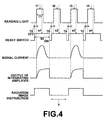
Figure 4 is a view showing a timing chart representing the
relation between the reading light beam projecting time and the
integrating time of the integrating amplifiers as the amplitude of
the signal current output from the linear electrodes of the radiation
image sensor and the amplitude of the output voltage of the
integrating amplifiers upon exposure to the reading light beam, in
the radiation image recording/read-out apparatus,
Figure 5 is a view showing a radiation image
recording/read-out apparatus in accordance with another embodiment
of the present invention,
Figure 6 is a view showing a form where the radiation image
sensor is connected to the integrating amplifier ICs,
Figure 7 is a view showing another form where the radiation
image sensor is connected to the integrating amplifier ICs,
Figure 8 is a view showing still another form where the
radiation image sensor is connected to the integrating amplifier
ICs, and
Figure 9 is a view showing a timing chart representing the
relation between the reading light beam projecting time and the
integrating time of the integrating amplifiers when the radiation
image is read out as well as the amplitude of the signal current
output from the linear electrodes of the radiation image sensor and
the amplitude of the output voltage of the integrating amplifiers
upon exposure to the reading light beam, in the prior art.
DESCRIPTION OF THE PREFERRED EMBODIMENTS
In Figure 1, a radiation image recording/read-out apparatus
in accordance with an embodiment of the present invention comprises
a radiation source (not shown), a radiation image sensor 10 on which
a radiation image is recorded upon exposure to radiation passing
through an object and which outputs charge signals according to the
radiation image recorded thereon, a reading light source portion
20 which causes a linear reading light beam to scan the radiation
image sensor 10, and an image signal detecting portion 30 which
integrates at each integrating time the charge signal output from
the radiation image sensor 10 in response to scan of the reading
light beam with integrating amplifiers 31 to be described later and
outputs the integrated image signal.
As shown in Figure 2, the radiation image sensor 10 comprises
a first electrode layer 11 permeable to radiation passing through
an object, a recording photoconductive layer 12 which generates
electric charges upon exposure to radiation passing through the first
electrode layer 11, a charge transfer layer 13 which behaves like
a substantially insulating material to the electric charges
generated in the recording photoconductive layer 12 and behaves like
a substantially conductive material to the electric charge in the
polarity opposite to that of the electric charges generated in the
recording photoconductive layer 12, a reading photoconductive layer
14 which generates electric charges upon exposure to reading light,
and a second electrode layer 15 in which a plurality of linear
electrodes 15a permeable to the reading light are arranged in
parallel to each other, the layers being superposed one on another
in this order. A charge accumulating portion 16 which accumulates
electric charges generated according to the amount of the projected
radiation is formed at the interface between the recording
photoconductive layer 12 and the charge transfer layer 13.
The reading light source portion 20 comprises a pulsed light
source 21 which emits, as the reading light, a pulsed light beam
which is projected onto the radiation image sensor 10 for a
predetermined time in each integrating time (by the integrating
amplifier 31) and a light emission control means 22 which controls
the light source 21. The radiation image sensor 10 and the reading
light source portion 20 are disposed so that the longitudinal
direction of the reading light source of the reading light source
portion 20 is substantially in perpendicular to the longitudinal
direction of the linear electrodes 15a of the radiation image sensor
10. Though the reading light source portion 20 causes the pulsed
reading light beam to scan the radiation image sensor 10 by moving
the pulsed light source 21 in the longitudinal direction of the linear
electrodes 15a, the mechanisms such as for moving the pulsed light
source 21 are not shown.
The light emission control means 22 controls projection of
the pulsed reading light beam so that the center of the time in which
the pulsed light beam is projected onto the radiation image sensor
10 is earlier than the center of the integrating time of the
integrating amplifier 31, as will be described in detail later.
The image signal detecting portion 30 comprises an integrating
amplifier 31 which integrates charge signals output from the
radiation image sensor 10, first and second sample hold circuits
32 and 33 which hold the output voltages output from the integrating
amplifier 31, a differential amplifier 34 which outputs the
difference between the output voltages respectively held by the first
and second sample hold circuits 32 and 33 as an image signal component,
and an A/D converter 35 which digitizes the analog image signal
component into a digital image signal component. It is preferred
that a low-pass filter be interposed between the integrating
amplifier 31 and the first and second sample hold circuits 32 and
33 in order to reduce noise.
The integrating amplifier 31 is provided with a capacitor 31a
which accumulates the charge signals output from the radiation image
sensor 10 and a reset switch 31b for causing the capacitor 31a to
discharge the charge signals accumulated therein.
The first and second sample hold circuits 32 and 33
respectively comprises switches 32a and 33a, capacitors 32b and 33b
which hold the output voltages output from the integrating amplifier
31, and buffer amplifiers 32c and 33c which output the output voltages
held by the capacitors 32b and 33b.
The operating timings of the reset switch 31b of the
integrating amplifier 31, the switches 32a and 33a of the first and
second sample hold circuits 32 and 33, and the A/D converter 35 are
controlled by a control circuit which is not shown.
In Figure 1 and the description above, only the image signal
detecting portion 30 connected to one of the linear electrodes 15a
of the radiation image sensor 10 is shown.
The A/D converter 35 may be provided for each linear electrode
15a or the analog image signal components output from the respective
differential amplifiers 34 may be sequentially input into one A/D
converter 35 through a multiplexer.
Operation of this radiation image recording/read-out
apparatus will be described, hereinbelow.
With the radiation image sensor 10 imparted with an electric
voltage so that the first electrode layer 11 is negatively charged
and the second electrode layer 15 is positively charged, radiation
L1 (Figure 3A) is projected onto the object 40 from the radiation
source. The radiation L1 radiated from the radiation source is
projected on the entire area of the object 40 and the radiation passing
through the radiation transmitting portion 40a of the object 40
impinges upon the radiation image sensor 10 from the first electrode
side while the radiation impinging upon the radiation shielding
potion 40b of the object 40 does not reach the radiation image sensor
10 as shown in Figure 3A.
The radiation L1 impinging upon the radiation image sensor
10 passes through the first electrode layer 11 and impinges upon
the recording photoconductive layer 12, whereby charged pairs are
generated in the recording photoconductive layer 12. The positive
charges of the charged pairs are combined with the negative charges
on the first electrode layer 11 and cancelled, whereas the negative
charges of the charged pairs are stored on the charge accumulating
portion 16 formed on the interface between the recording
photoconductive layer 12 and the charge transfer layer 12 as latent
image charges, whereby a radiation image is recorded on the radiation
image sensor 10.
Then with the first electrode layer 11 grounded, reading light
L2 is projected onto the radiation image sensor 10 from the second
electrode side.
Figure 4 shows a timing chart representing the relation
between the timing at which the reading light L2 is projected onto
the radiation image sensor 10 and the timing at which the reset switch
31b of the integrating amplifier 31 is turned on and off as well
as the amplitude of the signal current output from the linear
electrode 15a and the amplitude of the output voltage of the
integrating amplifier 31 upon exposure to the reading light beam
L2. It is assumed that a radiation image has been recorded on the
radiation image sensor in the distribution shown in Figure 4, that
is, linear images extending in the same direction as the pulsed light
source 21 are recorded in parallel at predetermined intervals in
the scanning direction of the pulsed light source 21, i.e., in the
direction of arrow Y in Figure 4.
As can be seen from Figure 4, the reset switch 31b of the
integrating amplifier 31 is opened (turned off) before the reading
light L2 is projected, and the integrating amplifier 31 is turned
into an integration initiating state. Then when a non-lighting time
T0 has lapsed after the integrating amplifier 31 initiates the
integration, the pulsed light source 21 is operated to emit the
reading light beam L2 under the control of a control signal from
the light emission control means 22. The reading light beam L2 is
emitted for a light emitting time T1 in each of the integrating times
S0 of the integrating amplifier 31 from the pulsed light source 21
and projected onto the radiation image sensor 10 as shown in Figure
4. The reading light beam L2 thus projected onto the radiation image
sensor 10 impinges upon the reading photoconductive layer 14 through
the linear electrodes 15a as shown in Figure 3B. The positive charges
generated in the reading photoconductive layer 14 upon exposure to
the reading light beam L2 are combined with the latent image charges
on the charge accumulating portion 16, while the negative charges
are combined with the positive charges on the linear electrode 15a
of the second electrode layer 15 and the charge signal according
to the amount of the combined charges is stored in the capacitor
31a of the integrating amplifier 31. When the integrating time S0
has lapsed, the charges stored in the capacitor 31a are discharged
and the capacitor 31a is reset. At this time, the pulsed light source
21 is controlled by the light emission control means 22 so that the
projection of the reading light beam L2 is stopped before the
integrating amplifier 31 is reset. Specifically, as shown in Figure
4, the light emission control means 22 controls the emission
initiating time and the light emitting time T1 of the pulsed light
source 21 so that the center t1 to t4 of each of the light emitting
times (for which the pulsed light beam is proj ected onto the radiation
image sensor) T1 is earlier than the center s1 to s4 of each of the
integrating times S0. That is, the time between the end of emission
of the reading light beam L2 and the end of the integration is longer
than the non-lighting time T0 between the initiation of the
integration and the initiation of emission of the reading light beam
L2.
Since the projection of the reading light beam is controlled
as described above, the output of the signal current from the
radiation image sensor 10 can be confined in the integrating time,
and the output of the integrating amplifier 31 corresponding to the
part where no radiation image is recorded can be nullified.
In this particular embodiment, the image signal is obtained
by correlation-double-sampling the output of the integrating
amplifier 31. Specifically, the switches 32a and 33a of the first
and second sample hold circuits 32 and 33 are short-circuited before
the reset switch 31b of the integrating amplifier 31 is opened.
(sample mode) Then immediately after the reset switch 31b of the
integrating amplifier 31 is opened (off) , the switch 32a of the first
sample hold circuit 32 is opened, whereby the output voltage of the
integrating amplifier 31 at that time is held by the capacitor 32b
of the first sample hold circuit 32. (hold mode) Then, subsequently,
immediately before the integrating time S0 lapses, the switch 33a
of the second sample hold circuit 33 is opened, whereby the output
voltage of the integrating amplifier 31 at that time is held by the
capacitor 33b of the second sample hold circuit 33. (hold mode)
Thereafter, the reset switch 31b of the integrating amplifier 31
is short-circuited and the electric charges stored in the capacitor
31a is discharged.
The output voltages thus held by the first and second sample
hold circuits 32 and 33 ate output to the differential amplifier
34 through the buffer amplifiers 32c and 33c. The differential
amplifier 34 calculates the difference between the two output
voltages and outputs the difference to the A/D converter 35. The
A/D converter 35 digitizes the differential signal input as an analog
signal and outputs as a digital signal.
After a digital signal is output from the A/D converter 35,
the switches 32a and 33a of the first and second sample hold circuits
32 and 33 are short-circuited, and the charges stored in the
capacitors 32b and 33b are discharged. Then the reset switch 31b
of the integrating amplifier 31 is opened again and integration is
started again.
In synchronization with the movement of the pulsed light
source 21 in the direction of the arrow Y in Figure 1, the projection
of the pulsed light and the integration by the integrating amplifier
31 described above are effected and finally a digital image signal
corresponding to the entire area of the radiation image sensor 10
is detected.
In the radiation image recording/read-out apparatus in
accordance this embodiment, since a pulsed light beam is employed
as the reading light beam and projection of the pulsed light beam
is controlled so that the center of the time in which the pulsed
light beam is projected onto the radiation image sensor is earlier
than the center of the integrating time, the signal current generated
in the radiation image sensor 10 in response to the pulsed light
projected onto the radiation image sensor in each integrating time
can be terminated within the integrating time without being continued
to the next integrating time, whereby generation of the noise due
to delay in response of the radiation image sensor 10 to the reading
light can be avoided and deterioration of the image quality such
as sharpness of the read-out image can be prevented.
Further, since in the radiation image recording/read-out
apparatus in accordance this embodiment, the emission initiating
time of the pulsed light beam by the pulsed light source is controlled
so that there is a non-lighting time T0, for which the reading light
beam is not lit, before the pulsed light beam is projected onto the
radiation image sensor in the integrating time, generation of the
offset voltage due to projection of the reading light just after
the initiation of the integration can be prevented and deterioration
of the S/N of the read radiation image can be prevented, e.g., when
the image signal is obtained through the correlation double sampling.
Further, though, in the image signal detecting portion 30 of
the embodiment described above, the first and second sample hold
circuits 32 and 33 are provided and so-called
correlation-double-sampling is effected, the processing of the image
signal detecting portion 30 need not be limited to the
correlation-double-sampling. For example, only one sample hold
circuit is provided and the output voltage of the integrating
amplifier held by the sample hold circuit 33 immediately before the
integrating time lapses may be obtained as the image signal
components. In this case, the control of the reading light emission
may be effected in the same manner as described above.
Though, in the embodiment described above, a radiation image
recording/read-out apparatus is formed by the radiation source, the
radiation image sensor 10, the reading light source portion 20 and
the image signal detecting portion 30, a radiation image read-out
apparatus may be formed by the radiation image sensor 10, the reading
light source portion 20 and the image signal detecting portion 30
without the radiation source or a radiation image read-out apparatus
may be formed by the reading light source portion 20 and the image
signal detecting portion 30 without the radiation source and the
radiation image sensor 10.
Further, when the outputs of the integrating amplifiers 31
connected to the respective linear electrodes 15a are switched by
the multiplexer and input into the A/D converter 36 in the embodiment
described above, so-called a TAB (Tape Automated Bonding) IC 60,
where an integrated amplifier IC 61 comprising integrated
integrating amplifiers 31 are loaded on a flexible substrate 62 such
as film, may be employed so that a plurality of linear electrodes
15a of the radiation image sensor 10 are connected to the TAB IC
60 and the outputs of the TAB ICs 60 are connected to the multiplexer
50 as shown in Figure 5.
When the TABIC 60 shown in Figure 5 is employed, it is preferred
that, for instance, the input lines to the TABIC 60 be wired at pitches
of 80 µm and the output lines therefrom be wired at pitches of 500 µm
to be matched with the downstream circuits as shown in Figure 6.
By wiring the TABIC 60 in the manner described above, for instance,
when the TABIC 60 is disposed in a radiation image sensor 10 for
recording a chest radiation image, the linear electrodes 15a provided
in the radiation image sensor 10 at pitches of 100 µm may be connected
to the TABIC 60 by converging the front end portions thereof as shown
in Figure 6, and when the TABIC 60 is disposed in a radiation image
sensor 10 for recording a chest radiation image (mammography), the
linear electrodes 15a provided in the radiation image sensor 10 at
pitches of 50 µm may be connected to the TABIC 60 by diverging the
front end portions as shown in Figure 7, whereby the TABIC 60 can
be employed in common in a radiation image sensor 10 for a chest
radiation image and a radiation image sensor 10 for a
the mammography and the part cost can be reduced.
When the TABIC 60 is disposed in a radiation image sensor 10
for the mammography, it is difficult to dispose the TABICs 60, to
which all the linear electrodes 15a are connected, on one side of
the radiation image sensor 10 because of the narrow spaces between
the linear electrodes 15a. Accordingly, the TABICs 60 may be
disposed alternately on opposite sides of the radiation image sensor
10 as shown in Figures 7 and 8. By disposing the TABICs 60 in the
manner described above, all the linear electrodes 15a can be
connected to the TABICs 60 even if the linear electrodes 15a are
provided at pitches smaller than those of the input lines to the
TABICs 60.