JP4246090B2 - Signal detection method and apparatus, and radiation image signal detection method and system - Google Patents
Signal detection method and apparatus, and radiation image signal detection method and system Download PDFInfo
- Publication number
- JP4246090B2 JP4246090B2 JP2004078415A JP2004078415A JP4246090B2 JP 4246090 B2 JP4246090 B2 JP 4246090B2 JP 2004078415 A JP2004078415 A JP 2004078415A JP 2004078415 A JP2004078415 A JP 2004078415A JP 4246090 B2 JP4246090 B2 JP 4246090B2
- Authority
- JP
- Japan
- Prior art keywords
- signal
- signal detection
- pass filter
- low
- charge
- Prior art date
- Legal status (The legal status is an assumption and is not a legal conclusion. Google has not performed a legal analysis and makes no representation as to the accuracy of the status listed.)
- Expired - Fee Related
Links
- 238000001514 detection method Methods 0.000 title claims description 73
- 230000005855 radiation Effects 0.000 title claims description 68
- 238000005070 sampling Methods 0.000 claims description 49
- 230000010354 integration Effects 0.000 claims description 32
- 238000009825 accumulation Methods 0.000 claims description 10
- 239000003990 capacitor Substances 0.000 description 17
- 238000000034 method Methods 0.000 description 10
- 230000002596 correlated effect Effects 0.000 description 8
- 230000008569 process Effects 0.000 description 8
- 238000006243 chemical reaction Methods 0.000 description 7
- 230000000875 corresponding effect Effects 0.000 description 6
- 238000005259 measurement Methods 0.000 description 5
- 230000004044 response Effects 0.000 description 4
- 230000001052 transient effect Effects 0.000 description 4
- 238000010586 diagram Methods 0.000 description 3
- 238000011156 evaluation Methods 0.000 description 2
- OAICVXFJPJFONN-UHFFFAOYSA-N Phosphorus Chemical compound [P] OAICVXFJPJFONN-UHFFFAOYSA-N 0.000 description 1
- 230000009471 action Effects 0.000 description 1
- 238000004458 analytical method Methods 0.000 description 1
- 230000005540 biological transmission Effects 0.000 description 1
- 230000015556 catabolic process Effects 0.000 description 1
- 230000008859 change Effects 0.000 description 1
- 239000004020 conductor Substances 0.000 description 1
- 230000001276 controlling effect Effects 0.000 description 1
- 238000006731 degradation reaction Methods 0.000 description 1
- 238000007599 discharging Methods 0.000 description 1
- 230000000694 effects Effects 0.000 description 1
- 238000001914 filtration Methods 0.000 description 1
- 239000012212 insulator Substances 0.000 description 1
- 238000004020 luminiscence type Methods 0.000 description 1
- 230000007246 mechanism Effects 0.000 description 1
- 230000003287 optical effect Effects 0.000 description 1
Images


Classifications
-
- H—ELECTRICITY
- H04—ELECTRIC COMMUNICATION TECHNIQUE
- H04N—PICTORIAL COMMUNICATION, e.g. TELEVISION
- H04N25/00—Circuitry of solid-state image sensors [SSIS]; Control thereof
- H04N25/60—Noise processing, e.g. detecting, correcting, reducing or removing noise
-
- H—ELECTRICITY
- H04—ELECTRIC COMMUNICATION TECHNIQUE
- H04N—PICTORIAL COMMUNICATION, e.g. TELEVISION
- H04N25/00—Circuitry of solid-state image sensors [SSIS]; Control thereof
- H04N25/60—Noise processing, e.g. detecting, correcting, reducing or removing noise
- H04N25/616—Noise processing, e.g. detecting, correcting, reducing or removing noise involving a correlated sampling function, e.g. correlated double sampling [CDS] or triple sampling
-
- H—ELECTRICITY
- H04—ELECTRIC COMMUNICATION TECHNIQUE
- H04N—PICTORIAL COMMUNICATION, e.g. TELEVISION
- H04N25/00—Circuitry of solid-state image sensors [SSIS]; Control thereof
- H04N25/60—Noise processing, e.g. detecting, correcting, reducing or removing noise
- H04N25/62—Detection or reduction of noise due to excess charges produced by the exposure, e.g. smear, blooming, ghost image, crosstalk or leakage between pixels
-
- H—ELECTRICITY
- H04—ELECTRIC COMMUNICATION TECHNIQUE
- H04N—PICTORIAL COMMUNICATION, e.g. TELEVISION
- H04N25/00—Circuitry of solid-state image sensors [SSIS]; Control thereof
- H04N25/60—Noise processing, e.g. detecting, correcting, reducing or removing noise
- H04N25/65—Noise processing, e.g. detecting, correcting, reducing or removing noise applied to reset noise, e.g. KTC noise related to CMOS structures by techniques other than CDS
-
- H—ELECTRICITY
- H04—ELECTRIC COMMUNICATION TECHNIQUE
- H04N—PICTORIAL COMMUNICATION, e.g. TELEVISION
- H04N5/00—Details of television systems
- H04N5/30—Transforming light or analogous information into electric information
-
- H—ELECTRICITY
- H01—ELECTRIC ELEMENTS
- H01L—SEMICONDUCTOR DEVICES NOT COVERED BY CLASS H10
- H01L27/00—Devices consisting of a plurality of semiconductor or other solid-state components formed in or on a common substrate
- H01L27/14—Devices consisting of a plurality of semiconductor or other solid-state components formed in or on a common substrate including semiconductor components sensitive to infrared radiation, light, electromagnetic radiation of shorter wavelength or corpuscular radiation and specially adapted either for the conversion of the energy of such radiation into electrical energy or for the control of electrical energy by such radiation
- H01L27/144—Devices controlled by radiation
- H01L27/146—Imager structures
- H01L27/14665—Imagers using a photoconductor layer
- H01L27/14676—X-ray, gamma-ray or corpuscular radiation imagers
Landscapes
- Engineering & Computer Science (AREA)
- Multimedia (AREA)
- Signal Processing (AREA)
- Measurement Of Radiation (AREA)
- Transforming Light Signals Into Electric Signals (AREA)
- Radiography Using Non-Light Waves (AREA)
- Solid State Image Pick-Up Elements (AREA)
- Facsimile Heads (AREA)
Description
本発明は、相関2重サンプリング処理を行う信号検出方法および装置並びに放射線画像信号検出方法およびシステムに関するものである。 The present invention relates to a signal detection method and apparatus for performing correlated double sampling processing, and a radiographic image signal detection method and system.
従来、光の照射を受けてその光を電荷信号に変換して出力するCCDやフォトマルチプライヤーなどの光電変換素子や、放射線の照射を受けて電荷を蓄積するとともに、該蓄積された電荷に応じた電荷信号を出力する放射線画像記録装置が様々な分野で利用されている。 Conventionally, a photoelectric conversion element such as a CCD or a photomultiplier that receives light irradiation and converts the light into a charge signal and outputs it, or accumulates charges upon receiving radiation, and according to the accumulated charges Radiation image recording apparatuses that output a charge signal are used in various fields.
そして、上記のような光電変換素子や放射線画像記録装置から出力された電荷信号を検出するものとして、IC化が可能であり、比較的ノイズが小さい積分アンプが一般的に用いられている。この積分アンプは、蓄積モードに切り替えることにより上記電荷信号の蓄積を開始し、リセットモードに切り替えられることにより蓄積された電荷信号を放電してその電荷量に応じた電気信号を出力するものである。 In order to detect the charge signal output from the photoelectric conversion element or the radiation image recording apparatus as described above, an integration amplifier that can be integrated into an IC and has relatively small noise is generally used. This integrating amplifier starts accumulation of the charge signal by switching to the accumulation mode, discharges the accumulated charge signal by switching to the reset mode, and outputs an electric signal corresponding to the amount of the charge. .
ここで、上記積分アンプの蓄積モードへの切り替えは、積分アンプにおけるリセットスイッチをON状態からOFF状態に切り替えることにより行われるが、このリセットスイッチの切替えによりリセットスイッチの有するkTCノイズが発生し、このノイズが信号成分の電気信号に含まれてしまう。そこで、このkTCノイズの影響を回避するために相関2重サンプリング処理が施される。相関2重サンプリング処理とは、積分アンプが蓄積モードに切り替わった後所定のベースラインサンプリング時間経過した時に出力される電気信号とリセットモードに切り替わる直前に出力される電気信号との差をとり、その差を信号成分とすることにより、上記kTCノイズの影響を回避することができる処理である。 Here, the integration amplifier is switched to the accumulation mode by switching the reset switch in the integration amplifier from the ON state to the OFF state. This switching of the reset switch generates kTC noise of the reset switch. Noise is included in the electrical signal of the signal component. Therefore, in order to avoid the influence of the kTC noise, a correlated double sampling process is performed. The correlated double sampling process is the difference between the electrical signal output when the predetermined baseline sampling time has elapsed after the integration amplifier switches to the accumulation mode and the electrical signal output immediately before switching to the reset mode. By using the difference as a signal component, the process can avoid the influence of the kTC noise.
そして、上記のような相関2重サンプリング処理を行う回路においては、積分アンプから出力される電気信号における高周波ノイズを低減するため積分アンプの後段にローパスフィルタが設けられており、積分アンプから出力された電気信号はこのローパスフィルタを通過して出力される。 In the circuit that performs the correlated double sampling processing as described above, a low-pass filter is provided after the integration amplifier in order to reduce high-frequency noise in the electrical signal output from the integration amplifier, and is output from the integration amplifier. The electrical signal passes through this low-pass filter and is output.
しかしながら、上記のようにローパスフィルタを設けた場合、ローパスフィルタは過渡応答を示すため、上記のように相関2重サンプリング処理を行う際のベースラインサンプリング時間が短すぎると、ノイズ成分の電気信号を十分な大きさで取得することができず、その結果、信号成分にノイズ成分が含まれてしまいS/Nの劣化を生じる。また、一般的には、ベースラインサンプリング時間は、信号検出の時間を短くするため、短い方が好ましく、たとえば、ローパスフィルタの時定数τに対して1τ〜2τ程度の時間とされており、上記のようなローパスフィルタの過渡応答まで考慮して設定された時間ではなかった。 However, when the low-pass filter is provided as described above, the low-pass filter exhibits a transient response. Therefore, if the baseline sampling time when performing the correlated double sampling processing as described above is too short, the electrical signal of the noise component is It cannot be acquired with a sufficient size, and as a result, a noise component is included in the signal component, resulting in degradation of S / N. In general, the baseline sampling time is preferably shorter in order to shorten the signal detection time. For example, the baseline sampling time is about 1τ to 2τ with respect to the time constant τ of the low-pass filter. It was not the time set in consideration of the transient response of the low-pass filter.
本発明は、上記事情に鑑み、相関2重サンプリング処理を行う信号検出方法および装置並びに放射線画像信号検出方法およびシステムにおいて、適切なベースラインサンプリング時間を設定することができ、信号成分のS/Nを向上することができる信号検出方法および装置並びに放射線画像信号検出方法およびシステムを提供することを目的とするものである。 In view of the above circumstances, the present invention can set an appropriate baseline sampling time in a signal detection method and apparatus and a radiographic image signal detection method and system for performing correlated double sampling processing, and can detect S / N of signal components. It is an object of the present invention to provide a signal detection method and apparatus and a radiological image signal detection method and system capable of improving the above.
本発明の信号検出方法は、積分アンプにより電荷信号の蓄積を開始し、その蓄積の開始から所定のベースラインサンプリング時間経過した時に積分アンプから出力され第1のローパスフィルタを通過した第1の電気信号を保持し、その第1の電気信号を保持した後積分アンプをリセットする前に積分アンプから出力され第2のローパスフィルタを通過した第2の電気信号と第1の電気信号との差を求めて信号検出する信号検出方法において、第1のローパスフィルタの時定数τおよびベースラインサンプリング時間tを、t≧10×τを満たすような値に設定することを特徴とする。 In the signal detection method of the present invention, accumulation of a charge signal is started by an integration amplifier, and when a predetermined baseline sampling time has elapsed from the start of the accumulation, the first electric signal output from the integration amplifier and passed through the first low-pass filter. The signal is held, and after the first electric signal is held, the difference between the first electric signal and the second electric signal output from the integrating amplifier and passed through the second low-pass filter before resetting the integrating amplifier is obtained. In the signal detection method of obtaining and detecting a signal, the time constant τ and the baseline sampling time t of the first low-pass filter are set to values satisfying t ≧ 10 × τ.
また、上記信号検出方法においては、第1のローパスフィルタの時定数τおよびベースラインサンプリング時間tを、20τ≧t≧10×τを満たすよう値に設定することができる。 In the signal detection method, the time constant τ and the baseline sampling time t of the first low-pass filter can be set to values that satisfy 20τ ≧ t ≧ 10 × τ.
本発明の信号検出装置は、電荷信号を蓄積する積分アンプと、その積分アンプによる電荷信号の蓄積の開始から所定のベースラインサンプリング時間経過した時に積分アンプから出力された信号が入力される第1のローパスフィルタと、第1のローパスフィルタを通過した第1の電気信号を保持する第1の保持回路と、その第1の保持回路により第1の電気信号が保持された後積分アンプをリセットする前に積分アンプから出力された信号が入力される第2のローパスフィルタと、第2のローパスフィルタを通過した第2の電気信号を保持する第2の保持回路と、第2の電気信号と第1の電気信号との差を求めて信号検出する差分回路とを備えた信号検出装置において、第1のローパスフィルタの時定数τおよびベースラインサンプリング時間tが、t≧10×τを満たすような値に設定されていることを特徴とする。 The signal detection device of the present invention includes an integration amplifier that accumulates a charge signal, and a signal that is output from the integration amplifier when a predetermined baseline sampling time has elapsed from the start of accumulation of the charge signal by the integration amplifier. The first low-pass filter, the first holding circuit that holds the first electric signal that has passed through the first low-pass filter, and the integration amplifier after the first electric signal is held by the first holding circuit is reset. A second low-pass filter to which a signal previously output from the integrating amplifier is input; a second holding circuit that holds the second electric signal that has passed through the second low-pass filter; a second electric signal; And a differential circuit that detects a signal by obtaining a difference from the electric signal of the first signal, the time constant τ of the first low-pass filter and the baseline sampling t, characterized in that it is set to a value that satisfies t ≧ 10 × τ.
また、上記信号検出装置においては、第1のローパスフィルタの時定数τおよびベースラインサンプリング時間tを、20×τ≧t≧10×τを満たすような値に設定することができる。 In the signal detection device, the time constant τ and the baseline sampling time t of the first low-pass filter can be set to values that satisfy 20 × τ ≧ t ≧ 10 × τ.
本発明の放射線画像信号検出方法は、放射線の照射を受けて電荷を蓄積するとともに、その蓄積された電荷に応じた電荷信号を出力する放射線画像記録装置から出力された電荷信号を、上記信号検出方法を用いて検出することを特徴とする。 The radiation image signal detection method of the present invention accumulates charges upon receiving radiation, and outputs a charge signal corresponding to the accumulated charges, and detects the charge signal output from the radiation image recording apparatus. It detects using the method, It is characterized by the above-mentioned.
本発明の放射線画像信号検出システムは、上記信号検出装置と、放射線の照射を受けて電荷を蓄積するとともに、その蓄積された電荷に応じた電荷信号を上記信号検出装置に出力する放射線画像記録装置とを備えたことを特徴とする。 The radiological image signal detection system of the present invention includes the signal detection device and a radiographic image recording device that accumulates charges upon receiving radiation and outputs a charge signal corresponding to the accumulated charges to the signal detection device. It is characterized by comprising.
ここで、上記「第1のローパスフィルタ」および上記「第2のローパスフィルタ」としては、共通のものを利用するようにしてもよいし、別々に設けるようにしてもよい。 Here, as the “first low-pass filter” and the “second low-pass filter”, common ones may be used, or they may be provided separately.
また、上記「第1のローパスフィルタ」および上記「第2のローパスフィルタ」としては、たとえば、1次フィルタを利用することができる。 Further, as the “first low-pass filter” and the “second low-pass filter”, for example, a primary filter can be used.
また、上記「第1の保持回路」および上記「第2の保持回路」としては、共通のものを利用するようにしてもよいし、別々に設けるようにしてもよい。 Further, as the “first holding circuit” and the “second holding circuit”, a common one may be used, or may be provided separately.
本発明の信号検出方法および装置並びに放射線画像信号検出方法およびシステムによれば、第1のローパスフィルタの時定数τおよびベースラインサンプリング時間tを、t≧10×τを満たすような値に設定するようにしたので、第1のローパスフィルタの過渡応答に対して十分なベースラインサンプリング時間を確保することができ、ノイズ成分の電気信号を十分な大きさで取得することができるので、信号成分にノイズ成分が混入することなく信号成分のS/Nの向上を図ることができる。 According to the signal detection method and apparatus and the radiographic image signal detection method and system of the present invention, the time constant τ and the baseline sampling time t of the first low-pass filter are set to values satisfying t ≧ 10 × τ. As a result, a sufficient baseline sampling time can be ensured for the transient response of the first low-pass filter, and the electrical signal of the noise component can be acquired with a sufficient magnitude. It is possible to improve the S / N of the signal component without mixing the noise component.
また、上記のように第1のローパスフィルタの時定数τおよびベースラインサンプリング時間tを、t≧10×τを満たすような値に設定すれば、たとえtを長くしたとしてもノイズ性能は変化しないが、tが大きくなるほど信号検出時間が長くなってしまい、その分放射線画像全体の読出サイクルが長くなり、放射線画像全体の画像信号を取得するまでの処理時間が長くなってしまう。そこで、上記信号検出方法および装置並びに放射線画像信号検出方法およびシステムにおいて、20×τ≧t≧10×τを満たすよう値に設定するようにした場合には、信号成分のS/Nの向上を図ることができるとともに、ある程度の処理スピードも確保することができる。 Further, as described above, if the time constant τ and the baseline sampling time t of the first low-pass filter are set to values satisfying t ≧ 10 × τ, the noise performance does not change even if t is increased. However, as t becomes larger, the signal detection time becomes longer, and accordingly, the readout cycle of the whole radiation image becomes longer, and the processing time until acquiring the image signal of the whole radiation image becomes longer. Therefore, in the above signal detection method and apparatus and radiographic image signal detection method and system, when the value is set so as to satisfy 20 × τ ≧ t ≧ 10 × τ, the S / N of the signal component is improved. It is possible to achieve a certain processing speed.
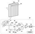
以下、図面を参照して本発明の信号検出方法を実施する信号検出装置の一実施形態を利用した放射線画像信号検出システムについて説明する。図1に、本発明の信号検出装置の一実施形態を利用した放射線画像信号検出システムの概略構成図を示す。 A radiation image signal detection system using an embodiment of a signal detection apparatus that performs a signal detection method of the present invention will be described below with reference to the drawings. FIG. 1 shows a schematic configuration diagram of a radiation image signal detection system using an embodiment of a signal detection apparatus of the present invention.
本放射線画像信号検出システムは、図示省略した放射線源と、放射線源から射出され、被写体を通過した放射線の照射を受けて放射線画像を記録し、その放射線画像に応じた電荷信号を出力する放射線画像記録装置10と、放射線画像記録装置10を線状の読取光で走査する読取光源部20と、読取光源部20による読取光の走査により放射線画像記録装置10から出力された電荷信号に基づいて上記放射線画像に応じたデジタル画像信号を出力する信号検出装置30とを備えている。
The radiation image signal detection system includes a radiation source (not shown), a radiation image that is emitted from the radiation source, receives radiation irradiated through the subject, records a radiation image, and outputs a charge signal corresponding to the radiation image. The
信号検出装置30は、放射線画像記録装置10から出力された電荷信号を積分する積分アンプ31、積分アンプ31により積分された電気信号を保持する第1および第2の保持回路32,33、第1および第2の保持回路32,33にそれぞれ保持された第1の電気信号および第2の電気信号の差分を出力する差分アンプ34、および差分アンプから出力されたアナログ信号をデジタル信号に変換するA/D変換器35を備えており、放射線画像記録装置10から出力された電荷信号に基づいて相関2重サンプリング処理を行うものである。
The
積分アンプ31は、放射線画像記録装置10から出力された電荷信号を蓄積するコンデンサ31aとコンデンサ31aに蓄積された電荷信号を放電させるためのリセットスイッチ31bとを備えている。
The
第1の保持回路32は、抵抗素子32aとスイッチ32bとコンデンサ32cとを備えている。そして、第1の保持回路32は積分アンプ31から出力された電気信号を保持するとともに、抵抗素子32aとコンデンサ32bとによって上記電気信号にローパスフィルタ処理を施すものである。したがって、第1の保持回路32のコンデンサ32cには、積分アンプ31から出力された電気信号にローパスフィルタ処理が施された、フィルタ処理済電気信号が保持される。
The
ここで、第1の保持回路32は、信号検出装置30において行われる相関2重サンプリング処理のベースラインサンプリングを行うものであるとともに、そのベースラインサンプリング信号となる積分アンプ31から出力された電気信号にローパスフィルタ処理を施すものである。そして、そのローパスフィルタ処理における時定数τとベースラインサンプリング時間tとは、t≧10×τを満たすような値に設定されている。つまり、τ=RCであるので、第1の保持回路32における抵抗素子32aの抵抗値Rとコンデンサ32bの容量Cとが、t≧10×RCを満たすように設定されている。なお、サンプリング時間tは後述する制御回路により制御される。
Here, the
第2の保持回路33は、抵抗素子33aとスイッチ33bとコンデンサ33cとを備えている。そして、第2の保持回路32は、上記第1の保持回路と同様に、積分アンプ31から出力された電気信号を保持するとともに、抵抗素子33aとコンデンサ33cとによって上記電気信号にローパスフィルタ処理を施すものである。したがって、第2の保持回路33のコンデンサ33cには、積分アンプ31から出力された電気信号にローパスフィルタ処理が施された、フィルタ処理済電気信号が保持される。
The
また、信号検出装置30は、第1および第2の保持回路32,33から出力されたフィルタ処理済電気信号を差分アンプ34に出力するバッファアンプ36,37と、積分アンプ31のリセットスイッチ31b、第1および第2の保持回路32,33のスイッチ32b,33bおよびA/D変換器35などの動作タイミングなどを制御する制御回路38とを備えている。
Further, the
放射線画像記録装置10は、詳細には、図2に示すように、放射線画像を担持した放射線を透過する第1の電極層11、第1の電極層11を透過した放射線の照射を受けることにより電荷を発生する記録用光導電層12、記録用光導電層12において発生した電荷に対しては絶縁体として作用し、且つその電荷と逆極性の輸送電荷に対しては導電体として作用する電荷輸送層13、読取光の照射を受けることにより電荷を発生する読取用光導電層14、および読取光を透過する線状に延びる線状電極15aが平行に配列された第2の電極層15をこの順に積層してなるものである。そして、記録用光導電層12と電荷輸送層13との界面には放射線の照射量に応じて発生した電荷が蓄積される蓄電部16が形成される。
In detail, as shown in FIG. 2, the radiographic image recording
また、図1においては、放射線画像記録装置10の1本の線状電極15aに接続される信号検出装置30のみを示しており、その他の線状電極15aに接続される信号検出装置30は図示省略してある。
In FIG. 1, only the
また、A/D変換器35は、各線状電極15aについてそれぞれ設けるようにしてもよいし、マルチプレクサを設けて差分アンプ34から出力されたアナログ信号を各線状電極毎に切り替えて1つのA/D変換器35に入力するようにしてもよい。
Further, the A /
なお、放射線画像記録装置10および読取光源部20は、上記読取光源部20の読取光源の長さ方向と放射線画像記録装置10の線状電極15aの長さ方向とが略直交するように設置されている。また、読取光源部20は、線状電極15aの長さ方向に線状の読取光源を移動させて読取光を走査するものであるが、読取光源を移動させる移動機構などについては図示省略してある。
The radiation
次に、本放射線画像信号検出システムの作用について説明する。 Next, the operation of the radiation image signal detection system will be described.
まず、放射線画像記録装置10の第1の電極層11が負に帯電し、第2の電極層15が正に帯電するように電圧印加された状態において、放射線源から被写体40に向けて放射線L1が照射される。放射線源から射出された放射線L1は、図3(A)に示すように、被写体40全体に照射され、被写体40において放射線を透過する透過部40aを透過した放射線が放射線画像記録装置10の第1の電極層11側から照射される。なお、被写体40において放射線を透過しない遮断部40bに照射された放射線は放射線画像記録装置10には照射されない。
First, in a state where a voltage is applied so that the
そして、放射線画像記録装置10に照射された放射線L1は、第1の電極層11を透過し、記録用光導電層12に照射される。そして、記録用光導電層12において放射線の照射により電荷対が発生し、そのうち正の電荷は第1の電極層11に帯電した負の電荷と結合して消滅し、負の電荷は潜像電荷として記録用光導電層12と電荷輸送層13との界面に形成される蓄電部16に蓄積されて放射線画像が記録される。
The radiation L1 irradiated to the radiation
そして、次に、図3(B)に示すように、第1の電極層11が接地された状態において、第2の電極層15側から読取光L2が照射され、読取光L2は線状電極15aを透過して読取用光導電層14に照射される。読取光L2の照射により読取用光導電層14において発生した正の電荷が蓄電部16における潜像電荷と結合するとともに、負の電荷が第2の電極層15の線状電極15aに帯電した正の電荷と結合する。
Then, as shown in FIG. 3B, in the state where the
一方、信号検出装置30における積分アンプ31のリセットスイッチ31bは、上記放射線画像記録装置10への読取光の照射の前にはON状態にされており、読取光の照射が開始されるとOFF状態にされ、上記のようにして放射線画像記録装置10の読取用光導電層14において発生した負の電荷が第2の電極層15の線状電極15aに帯電した正の電荷と結合することにより、その結合した電荷量に応じた大きさの電荷信号が積分アンプ31のコンデンサ31aに蓄積される。
On the other hand, the
そして、第1および第2の保持回路32,33のスイッチ32b,33bは、図4に示すように、積分アンプ31のリセットスイッチ31bがOFF状態にされる前にはON状態となっている。そして、積分アンプ31のリセットスイッチ31bがOFF状態にされて積分アンプ31による電荷信号の蓄積が開始された後、所定のベースラインサンプリング時間tが経過した時、第1の保持回路32のスイッチ32bがOFF状態にされ、積分アンプ31から出力されローパスフィルタ処理の施された第1のフィルタ処理済電気信号がコンデンサ32cにより保持される。そして、その第1のフィルタ処理済電気信号が保持され、所定のサンプリング時間が経過した後積分アンプ31をリセットする直前に第2の保持回路33のスイッチ33bがOFF状態にされ、積分アンプ31から出力されローパスフィルタ処理の施された第2のフィルタ処理済電気信号がコンデンサ33cにより保持される。
As shown in FIG. 4, the
そして、第1の保持回路32のコンデンサ32cに保持された第1のフィルタ処理済電気信号および第2の保持回路33に保持された第2のフィルタ処理済電気信号は、それぞれバッファアンプ36,37を介して差動アンプ34に出力される。そして、差動アンプ34において上記2つのフィルタ処理済電気信号の差分が算出され、A/D変換器35に出力される。A/D変換器35は、入力されたアナログ画像信号である差分信号をデジタル変換してデジタル画像信号として出力する。
The first filtered electric signal held in the
読取光源部20の1ラインの照射に対し、上記のような画像信号の検出が各線状電極15aに接続された信号検出回路30毎に行われて1ライン分の画像信号の検出が行われる。そして、読取光源部20により線状の読取光が、図1の矢印Y方向に走査されるのと同期して上記1ライン分の画像信号の検出がそれぞれ行われ、最終的には放射線画像記録装置10の全面分のデジタル画像信号が検出される。
For the irradiation of one line of the reading
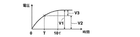
ここで、上記のようにして得られるデジタル画像信号は、差分アンプ34により第2のフィルタ処理済電気信号から第1のフィルタ処理済電気信号を差し引いたものであり、第1のフィルタ処理済電気信号は、上記のようにベースラインサンプリング時間tの間に第1の保持回路32のコンデンサ32cにより保持されるものである。そして、第1の保持回路32は、上述したようにローパスフィルタとしても動作するため、コンデンサ32cにより保持される電気信号の電圧は、図5に示すように、過渡応答を示す。したがって、ベースラインサンプリング時間が短すぎると、たとえば、図5に示す時間Tをベースラインサンプリング時間とすると、本来、第1のフィルタ処理済電気信号としては、電圧V1の大きさの信号が得られるところ、電圧V2の大きさの信号しか得ることしかできず、その結果、第2のフィルタ処理済電気信号から差し引かれる第1のフィルタ処理済電気信号の大きさが小さくなってしまい、ノイズ成分が含まれたデジタル画像信号が出力されてしまうことになる。
Here, the digital image signal obtained as described above is obtained by subtracting the first filtered electric signal from the second filtered electric signal by the
そこで、本実施形態の信号検出装置では、適切なベースラインサンプリング時間tを確保するために、上述したようにローパスフィルタ処理における時定数τとベースラインサンプリング時間tとが、t≧10×τを満たすような値に設定されている。 Therefore, in the signal detection device of the present embodiment, in order to ensure an appropriate baseline sampling time t, as described above, the time constant τ and the baseline sampling time t in the low-pass filter processing satisfy t ≧ 10 × τ. The value is set to satisfy.
ここで、t≧10×τとするのが適切なことを示すデータを以下に示す。 Here, data indicating that it is appropriate to satisfy t ≧ 10 × τ is shown below.
まず、図1に示す信号検出装置30の積分アンプ31の入力端を開放した状態で、積分アンプ31の入力換算ノイズ電子数ENCを測定した結果を図6(A)に示す。図6(A)には、ローパスフィルタ処理の時定数τを20μs、70μsおよび200μsとしたときのベースラインサンプリング時間とENCとの関係を示したものである。なお、ENCとは、入力換算電子数Nの標準偏差であり、入力換算電子数Nとは、以下の式から求められるものである。上記のようにENCを評価することにより、信号検出装置30から出力される信号における積分アンプ31のノイズ成分の大きさを評価することができる。
First, FIG. 6A shows a result of measuring the input conversion noise electron number ENC of the
N=Cf×Vad×x/q×G×2n
ただし、q:電荷素量(1.6×10⁻¹⁹(C))
Cf:積分アンプ帰還容量
G:積分アンプ後のゲイン
Vad:A/D変換器入力電圧レンジ
n:A/D変換器ビット数
x:A/D変換器出力デジタルデータ
そして、図6(A)に示すように、τ=20μsの場合には、ベースラインサンプリング時間がほぼ200μs以上でENCがほぼ最小になっており、τ=70μsの場合には、ベースラインサンプリング時間がほぼ700μs以上でENCがほぼ最小になっており、τ=200μsの場合には、ベースラインサンプリング時間がほぼ2000μs以上でENCがほぼ最小になっており、ベースラインサンプリング時間がt≧10×τのときに信号検出装置30から出力されるデジタル画像信号のノイズ成分が最も小さくなることを示している。また、図6(B)は、図6(A)の測定データを時定数τおよび10×τの時のENCで規格化したものである。図6(B)からもt≧10×τのときにENCが最小になることが明らかである。
N = C f × V ad × x / q × G × 2 n
Where q: elementary charge (1.6 × 10 −19 (C))
C f : Integration amplifier feedback capacity G: Gain after integration amplifier V ad : A / D converter input voltage range n: Number of bits of A / D converter x: A / D converter output digital data ), When τ = 20 μs, the ENC is almost minimum when the baseline sampling time is approximately 200 μs or more. When τ = 70 μs, the ENC is approximately 700 μs or more. When τ = 200 μs, the baseline sampling time is approximately 2000 μs or more and ENC is substantially minimum. When the baseline sampling time is t ≧ 10 × τ, the
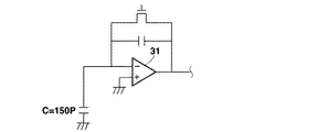
次に、図1に示す信号検出装置30の積分アンプ31の入力端に所定の負荷を付けた場合における積分アンプ31の入力換算ノイズ電子数ENCを測定した結果を図7(A)に示す。なお、図7(A)においては、上記入力端がNo load(開放状態)である場合と、上記入力端に図8に示すように、コンデンサC=150pを付けた場合と、上記入力端に図9に示すように、コンデンサC=150pおよび抵抗素子R=200kΩと付けた場合とで測定した結果を示している。なお、ローパスフィルタ処理の時定数τは70μsに設定している。なお、上記のように負荷を付けるのは、信号検出装置30に放射線画像記録装置10の線状電極15aなどを接続した場合を想定するためである。
Next, FIG. 7A shows the result of measuring the input conversion noise electron number ENC of the
図7(A)に示すように、全てzの負荷状態において、ベースラインサンプリング時間が700μs以上でENCが最小となっており、上記入力端に接続される負荷状態にかかわらず、t≧10×τのときに信号検出装置30から出力されるデジタル画像信号のノイズが最も小さくなることを示している。また、図7(B)は、図7(A)の測定データを時定数τ=70μsおよび10×τ=700μsの時のENCで規格化したものである。図7(B)からも、負荷状態にかかわらずt≧10×τのときにENCが最小になることが明らかである。
As shown in FIG. 7A, in all the z load states, the baseline sampling time is 700 μs or more and ENC is minimum, and t ≧ 10 × regardless of the load state connected to the input terminal. It shows that the noise of the digital image signal output from the
上記放射線画像信号検出システムによれば、ローパスフィルタの時定数τおよびベースラインサンプリング時間tを、t≧10×τを満たすような値に設定するようにしたので、ローパスフィルタの過渡応答に対して十分なベースラインサンプリング時間を確保することができ、ノイズ成分の電気信号を十分な大きさで取得することができるので、信号成分にノイズ成分が混入することなく信号成分のS/Nの向上を図ることができる。 According to the radiation image signal detection system, the time constant τ and the baseline sampling time t of the low-pass filter are set to values that satisfy t ≧ 10 × τ. Sufficient baseline sampling time can be ensured, and the noise component electrical signal can be acquired with a sufficient size, so that the S / N of the signal component can be improved without mixing the noise component into the signal component. You can plan.
また、上記実施形態においては、ローパスフィルタの時定数τおよびベースラインサンプリング時間tを、t≧10×τを満たすような値に設定するようにしたが、20×τ≧t≧10×τとするのが望ましい。上記のようにローパスフィルタの時定数τおよびベースラインサンプリング時間tを設定することにより、信号成分のS/Nの向上を図ることができるとともに、ある程度の処理スピードも確保することができる。 In the above embodiment, the time constant τ and the baseline sampling time t of the low-pass filter are set to values that satisfy t ≧ 10 × τ, but 20 × τ ≧ t ≧ 10 × τ. It is desirable to do. By setting the time constant τ and the baseline sampling time t of the low-pass filter as described above, the S / N of the signal component can be improved and a certain processing speed can be secured.
また、上記実施形態においては、信号検出装置に入力される電荷信号を出力するものとして、いわゆる光読取方式の放射線画像検出器を用いたもの説明したが、これに限らず、たとえば、いわゆるTFT方式の放射線画像検出器を用いるようにしてもよいし、また、蓄積性蛍光体シートから発せられた輝尽発光光を光電変換素子により検出して電荷信号を出力する放射線画像検出器を用いるようにしてもよい。 Further, in the above-described embodiment, the description has been made using the so-called optical reading type radiation image detector as the output of the charge signal input to the signal detection device. However, the present invention is not limited to this. The radiation image detector may be used, or a radiation image detector that outputs a charge signal by detecting the photostimulated luminescence emitted from the stimulable phosphor sheet by a photoelectric conversion element may be used. May be.
また、上記実施形態においては、放射線源、放射線画像記録装置10、読取光源部20および信号検出装置30から放射線画像信号検出システムを構成するようにしたが、放射線源を設けずに放射線画像記録装置10、読取光源部20および信号検出装置30から放射線画像信号検出システムを構成するようにしてもよい。
In the above embodiment, the radiation image signal detection system is configured by the radiation source, the radiation
10 放射線画像記録装置
11 第1の電極層
12 記録用光導電層
13 電荷輸送層
14 読取用光導電層
15 第2の電極層
16 蓄電部
20 読取光源部
30 信号検出装置
31 積分アンプ
32 第1の保持回路
33 第2の保持回路
34 差分アンプ
35 A/D変換器
38 制御回路
40 被写体
DESCRIPTION OF
Claims (6)
前記第1のローパスフィルタの時定数τおよび前記ベースラインサンプリング時間tを、t≧10×τを満たすような値に設定することを特徴とする信号検出方法。 The integration amplifier starts accumulating the charge signal, holds the first electric signal output from the integration amplifier and passed through the first low-pass filter when a predetermined baseline sampling time elapses from the start of the accumulation, Signal detection by obtaining a difference between the first electric signal and the second electric signal output from the integrating amplifier and passed through the second low-pass filter before the integrating amplifier is reset after holding the electric signal of 1 In the signal detection method to
A signal detection method, wherein the time constant τ of the first low-pass filter and the baseline sampling time t are set to values satisfying t ≧ 10 × τ.
前記第1のローパスフィルタの時定数τおよび前記ベースラインサンプリング時間tが、t≧10×τを満たすような値に設定されていることを特徴とする信号検出装置。 An integration amplifier for accumulating a charge signal; a first low-pass filter to which a signal output from the integration amplifier is input when a predetermined baseline sampling time has elapsed from the start of accumulation of the charge signal by the integration amplifier; A first holding circuit that holds a first electric signal that has passed through one low-pass filter, and the integration before the integration amplifier is reset after the first electric signal is held by the first holding circuit. A second low-pass filter to which the signal output from the amplifier is input; a second holding circuit that holds the second electric signal that has passed through the second low-pass filter; the second electric signal; A signal detection device including a difference circuit that detects a difference from an electrical signal of 1 and detects a signal;
The signal detection device, wherein the time constant τ of the first low-pass filter and the baseline sampling time t are set to values satisfying t ≧ 10 × τ.
放射線の照射を受けて電荷を蓄積するとともに、該蓄積された電荷に応じた電荷信号を前記信号検出装置に出力する放射線画像記録装置とを備えたことを特徴とする放射線画像信号検出システム。
A signal detection device according to claim 3 or 4,
A radiation image signal detection system comprising: a radiation image recording device that accumulates charges upon irradiation of radiation and outputs a charge signal corresponding to the accumulated charges to the signal detection device.
Priority Applications (2)
| Application Number | Priority Date | Filing Date | Title |
|---|---|---|---|
| JP2004078415A JP4246090B2 (en) | 2004-03-18 | 2004-03-18 | Signal detection method and apparatus, and radiation image signal detection method and system |
| US11/081,661 US7257500B2 (en) | 2004-03-18 | 2005-03-17 | Signal detecting method and device, and radiation image signal detecting method and system |
Applications Claiming Priority (1)
| Application Number | Priority Date | Filing Date | Title |
|---|---|---|---|
| JP2004078415A JP4246090B2 (en) | 2004-03-18 | 2004-03-18 | Signal detection method and apparatus, and radiation image signal detection method and system |
Publications (3)
| Publication Number | Publication Date |
|---|---|
| JP2005269215A JP2005269215A (en) | 2005-09-29 |
| JP2005269215A5 JP2005269215A5 (en) | 2006-06-15 |
| JP4246090B2 true JP4246090B2 (en) | 2009-04-02 |
Family
ID=34987430
Family Applications (1)
| Application Number | Title | Priority Date | Filing Date |
|---|---|---|---|
| JP2004078415A Expired - Fee Related JP4246090B2 (en) | 2004-03-18 | 2004-03-18 | Signal detection method and apparatus, and radiation image signal detection method and system |
Country Status (2)
| Country | Link |
|---|---|
| US (1) | US7257500B2 (en) |
| JP (1) | JP4246090B2 (en) |
Families Citing this family (10)
| Publication number | Priority date | Publication date | Assignee | Title |
|---|---|---|---|---|
| JP4448042B2 (en) * | 2005-02-17 | 2010-04-07 | 富士フイルム株式会社 | Signal detection method and apparatus, and radiation image signal detection method and system |
| JP4854972B2 (en) * | 2005-03-08 | 2012-01-18 | 富士フイルム株式会社 | Signal detection device |
| WO2007055114A1 (en) * | 2005-11-08 | 2007-05-18 | Matsushita Electric Industrial Co., Ltd. | Correlating double sampling circuit and sample hold circuit |
| JP2008177387A (en) * | 2007-01-19 | 2008-07-31 | Fujifilm Corp | Radiation image detector |
| EP2180599B1 (en) | 2008-10-24 | 2014-12-17 | Advanced Silicon SA | X-ray imaging readout and system |
| JP5324947B2 (en) * | 2009-02-03 | 2013-10-23 | 浜松ホトニクス株式会社 | Signal processing apparatus and light detection apparatus |
| WO2011119466A2 (en) * | 2010-03-22 | 2011-09-29 | Hologic Inc. | Decorrelated channel sampling for digital imaging |
| EP2617132B1 (en) * | 2010-09-14 | 2020-12-02 | Advanced Silicon SA | Circuit for capacitive touch applications |
| US20140049291A1 (en) * | 2012-08-14 | 2014-02-20 | Luxen Technologies, Inc. | Noise-resistant sampling circuit and image sensor |
| KR20160067251A (en) * | 2014-12-03 | 2016-06-14 | 삼성디스플레이 주식회사 | Orgainic light emitting display and driving method for the same |
Family Cites Families (4)
| Publication number | Priority date | Publication date | Assignee | Title |
|---|---|---|---|---|
| JPS6037660B2 (en) * | 1980-05-06 | 1985-08-27 | 日本ビクター株式会社 | Approximate compression method for audio signals |
| JP4619640B2 (en) * | 2003-10-10 | 2011-01-26 | 富士フイルム株式会社 | Signal detection method and apparatus |
| JP4265964B2 (en) * | 2003-11-12 | 2009-05-20 | 富士フイルム株式会社 | Radiation image reading method and apparatus |
| JP4037381B2 (en) * | 2004-03-31 | 2008-01-23 | 富士フイルム株式会社 | Optical information reading method and apparatus |
-
2004
- 2004-03-18 JP JP2004078415A patent/JP4246090B2/en not_active Expired - Fee Related
-
2005
- 2005-03-17 US US11/081,661 patent/US7257500B2/en active Active
Also Published As
| Publication number | Publication date |
|---|---|
| JP2005269215A (en) | 2005-09-29 |
| US20050209803A1 (en) | 2005-09-22 |
| US7257500B2 (en) | 2007-08-14 |
Similar Documents
| Publication | Publication Date | Title |
|---|---|---|
| USRE49401E1 (en) | Radiation imaging apparatus and radiation imaging system | |
| US7257500B2 (en) | Signal detecting method and device, and radiation image signal detecting method and system | |
| KR101842259B1 (en) | Image sensor and X-ray image sensing module including the same | |
| US11303831B2 (en) | Radiation imaging apparatus and radiation imaging method | |
| US9971046B2 (en) | Radiation imaging apparatus and radiation imaging system | |
| US10441238B2 (en) | Radiation imaging apparatus, control method thereof, and program | |
| JP4448042B2 (en) | Signal detection method and apparatus, and radiation image signal detection method and system | |
| JP6087780B2 (en) | Image sensor, radiation detection apparatus, and image sensor control method | |
| US20140239186A1 (en) | Radiation imaging apparatus, radiation inspection apparatus, method for correcting signal, and computer-readable storage medium | |
| US7659518B2 (en) | Light or radiation image pickup apparatus | |
| WO2020241062A1 (en) | Radiographic imaging device and radiographic imaging system | |
| GB2543377A (en) | Radiation imaging apparatus, radiation imaging system, and irradiation start detection method | |
| JP4403045B2 (en) | Radiation image detector | |
| JP2003153088A (en) | Signal detecting method and device | |
| JP4619640B2 (en) | Signal detection method and apparatus | |
| JP4854972B2 (en) | Signal detection device | |
| JP7441033B2 (en) | Radiation imaging devices and radiation imaging systems | |
| JP4265964B2 (en) | Radiation image reading method and apparatus | |
| JP7441032B2 (en) | Radiation imaging devices and radiation imaging systems | |
| JP7319809B2 (en) | Radiation imaging apparatus, its control method, and radiation imaging system | |
| US20240069222A1 (en) | Radiation imaging apparatus and radiation imaging system | |
| JP2009088774A (en) | Signal detecting apparatus, signal detecting system, radiographic image signal detecting system, signal detecting method and radiographic image signal detecting method | |
| JP2022174661A (en) | Radiation imaging device and radiation imaging system | |
| JP2021040195A (en) | Radiation imaging apparatus, radiation imaging system, and processing method of radiation imaging apparatus | |
| JP2005164415A (en) | Radiological image reading device and detector |
Legal Events
| Date | Code | Title | Description |
|---|---|---|---|
| A521 | Request for written amendment filed |
Free format text: JAPANESE INTERMEDIATE CODE: A523 Effective date: 20060428 |
|
| A621 | Written request for application examination |
Free format text: JAPANESE INTERMEDIATE CODE: A621 Effective date: 20060428 |
|
| A711 | Notification of change in applicant |
Free format text: JAPANESE INTERMEDIATE CODE: A712 Effective date: 20061207 |
|
| A977 | Report on retrieval |
Free format text: JAPANESE INTERMEDIATE CODE: A971007 Effective date: 20081210 |
|
| TRDD | Decision of grant or rejection written | ||
| A01 | Written decision to grant a patent or to grant a registration (utility model) |
Free format text: JAPANESE INTERMEDIATE CODE: A01 Effective date: 20090106 |
|
| A01 | Written decision to grant a patent or to grant a registration (utility model) |
Free format text: JAPANESE INTERMEDIATE CODE: A01 |
|
| A61 | First payment of annual fees (during grant procedure) |
Free format text: JAPANESE INTERMEDIATE CODE: A61 Effective date: 20090107 |
|
| R150 | Certificate of patent or registration of utility model |
Ref document number: 4246090 Country of ref document: JP Free format text: JAPANESE INTERMEDIATE CODE: R150 Free format text: JAPANESE INTERMEDIATE CODE: R150 |
|
| FPAY | Renewal fee payment (event date is renewal date of database) |
Free format text: PAYMENT UNTIL: 20120116 Year of fee payment: 3 |
|
| FPAY | Renewal fee payment (event date is renewal date of database) |
Free format text: PAYMENT UNTIL: 20120116 Year of fee payment: 3 |
|
| FPAY | Renewal fee payment (event date is renewal date of database) |
Free format text: PAYMENT UNTIL: 20130116 Year of fee payment: 4 |
|
| R250 | Receipt of annual fees |
Free format text: JAPANESE INTERMEDIATE CODE: R250 |
|
| FPAY | Renewal fee payment (event date is renewal date of database) |
Free format text: PAYMENT UNTIL: 20130116 Year of fee payment: 4 |
|
| FPAY | Renewal fee payment (event date is renewal date of database) |
Free format text: PAYMENT UNTIL: 20140116 Year of fee payment: 5 |
|
| R250 | Receipt of annual fees |
Free format text: JAPANESE INTERMEDIATE CODE: R250 |
|
| R250 | Receipt of annual fees |
Free format text: JAPANESE INTERMEDIATE CODE: R250 |
|
| R250 | Receipt of annual fees |
Free format text: JAPANESE INTERMEDIATE CODE: R250 |
|
| R250 | Receipt of annual fees |
Free format text: JAPANESE INTERMEDIATE CODE: R250 |
|
| R250 | Receipt of annual fees |
Free format text: JAPANESE INTERMEDIATE CODE: R250 |
|
| R250 | Receipt of annual fees |
Free format text: JAPANESE INTERMEDIATE CODE: R250 |
|
| R250 | Receipt of annual fees |
Free format text: JAPANESE INTERMEDIATE CODE: R250 |
|
| LAPS | Cancellation because of no payment of annual fees |