EP1537709B1 - Method for generating a digital i/q signal in a tdma transmitter and corresponding modulator - Google Patents
Method for generating a digital i/q signal in a tdma transmitter and corresponding modulator Download PDFInfo
- Publication number
- EP1537709B1 EP1537709B1 EP03791136.9A EP03791136A EP1537709B1 EP 1537709 B1 EP1537709 B1 EP 1537709B1 EP 03791136 A EP03791136 A EP 03791136A EP 1537709 B1 EP1537709 B1 EP 1537709B1
- Authority
- EP
- European Patent Office
- Prior art keywords
- modulator
- pulse
- shaping filter
- digital
- gmsk
- Prior art date
- Legal status (The legal status is an assumption and is not a legal conclusion. Google has not performed a legal analysis and makes no representation as to the accuracy of the status listed.)
- Expired - Lifetime
Links
- 238000000034 method Methods 0.000 title claims description 5
- 238000007493 shaping process Methods 0.000 claims description 38
- 238000003672 processing method Methods 0.000 claims description 4
- 238000004590 computer program Methods 0.000 claims description 3
- 230000001419 dependent effect Effects 0.000 claims 1
- 238000013507 mapping Methods 0.000 claims 1
- 230000007704 transition Effects 0.000 description 5
- VYPSYNLAJGMNEJ-UHFFFAOYSA-N Silicium dioxide Chemical compound O=[Si]=O VYPSYNLAJGMNEJ-UHFFFAOYSA-N 0.000 description 4
- 230000000694 effects Effects 0.000 description 3
- 230000005540 biological transmission Effects 0.000 description 2
- 238000010586 diagram Methods 0.000 description 2
- 238000012545 processing Methods 0.000 description 2
- 238000005070 sampling Methods 0.000 description 2
- 230000001052 transient effect Effects 0.000 description 2
- 238000004891 communication Methods 0.000 description 1
- 238000000354 decomposition reaction Methods 0.000 description 1
- 230000007547 defect Effects 0.000 description 1
- 238000013461 design Methods 0.000 description 1
- 238000001914 filtration Methods 0.000 description 1
- 238000010295 mobile communication Methods 0.000 description 1
- 230000010363 phase shift Effects 0.000 description 1
- 230000000979 retarding effect Effects 0.000 description 1
- 229920006395 saturated elastomer Polymers 0.000 description 1
- 230000003595 spectral effect Effects 0.000 description 1
- 238000012546 transfer Methods 0.000 description 1
Images


Classifications
-
- H—ELECTRICITY
- H04—ELECTRIC COMMUNICATION TECHNIQUE
- H04L—TRANSMISSION OF DIGITAL INFORMATION, e.g. TELEGRAPHIC COMMUNICATION
- H04L27/00—Modulated-carrier systems
- H04L27/18—Phase-modulated carrier systems, i.e. using phase-shift keying
- H04L27/20—Modulator circuits; Transmitter circuits
-
- H—ELECTRICITY
- H04—ELECTRIC COMMUNICATION TECHNIQUE
- H04L—TRANSMISSION OF DIGITAL INFORMATION, e.g. TELEGRAPHIC COMMUNICATION
- H04L27/00—Modulated-carrier systems
- H04L27/0008—Modulated-carrier systems arrangements for allowing a transmitter or receiver to use more than one type of modulation
-
- H—ELECTRICITY
- H04—ELECTRIC COMMUNICATION TECHNIQUE
- H04L—TRANSMISSION OF DIGITAL INFORMATION, e.g. TELEGRAPHIC COMMUNICATION
- H04L27/00—Modulated-carrier systems
- H04L27/18—Phase-modulated carrier systems, i.e. using phase-shift keying
- H04L27/20—Modulator circuits; Transmitter circuits
- H04L27/2003—Modulator circuits; Transmitter circuits for continuous phase modulation
- H04L27/2007—Modulator circuits; Transmitter circuits for continuous phase modulation in which the phase change within each symbol period is constrained
- H04L27/2017—Modulator circuits; Transmitter circuits for continuous phase modulation in which the phase change within each symbol period is constrained in which the phase changes are non-linear, e.g. generalized and Gaussian minimum shift keying, tamed frequency modulation
Definitions
- the present invention relates to a modulator for generating a digital I/Q signal having a plurality of time-slots, to a signal processing method for generating a digital I/Q signal having a plurality of time-slots and to a computer program for a time division multiple access (TDMA) transmitter for a global system for mobile communications (GSM), enhanced data rates for GSM evolution (EDGE) or enhanced general packet radio service (EGPRS) system.
- GSM global system for mobile communications
- EDGE enhanced data rates for GSM evolution
- GPRS enhanced general packet radio service
- EGPRS European Standardization Institute
- GMSK Gaussian minimum shift keying
- This new 8PSK modulation scheme has more stringent requirements with respect to the linearity of the power amplifier in the TX (transmission) chain since, in contrast to GMSK, the amplitude is not constant. Therefore, while the constant envelope of the GMSK enabled the employment of a saturated power amplifier (PA), which is more power efficient than a linear PA, the variable envelope of the 8PSK modulation scheme demands for a linear PA.
- PA saturated power amplifier
- the 8PSK modulation scheme is employed in multi-time slot (TS) operation. It is required to adjust the TX power for every TS individually as demanded by the BSC.
- the TX power transient between the TSs should be smooth. Otherwise, if the TX power transient between the TSs is not smooth, interferences may occur with other users on adjacent channels. Due to this, it is normally not possible to simply switch the gain of the TX path abruptly. In addition to that, the gain of the TX path is usually varied in the analogue domain. Due to this, a continuous variable gain amplifier (VGA) is required in the TX chain, for adjusting the TX power level. Such a VGA is controlled by an appropriately shaped analogue control voltage.
- VGA continuous variable gain amplifier
- guard interval The requirement for smooth TX power ramping is fundamental to any multiple access system, which combines TDMA and frequency division multiple access (FDMA). Therefore, the applied standards reserve a time interval between adjacent TSs, which is dedicated to power ramping and in which no data transfer occurs. According to the GSM standard, this time interval is denoted as "guard interval”.
- the power ramping voltage has a step shape with smooth edges.
- VANKKA J ET AL "A GSM/EDGE/WCDMA modulator with on-chip D/A converter for base station”,IEEE INTERNATIONAL SOLID-STATE CIRCUITS CONFERENCE.
- DIGEST OF TECHNICAL PAPERS, SAN FRANCISCO, USA, vol. 1, 5 February 2002 (2002-02-05), pages 236-463 discloses a modulator which allows power ramping on a time-slot basis. It is an object of the present invention to minimize interferences between adjacent time slots.
- this object is solved with a modulator for generating a digital I/Q signal having a plurality of time slots, the modulator comprising means for introducing a dip in an envelope of the digital I/Q signal in a guard interval between adjacent time slots of the plurality of time slots.
- Such modulator according to an exemplary embodiment of the present invention as set forth in claim 1 allows the use of a linear power amplifier in the digital I/Q modulator supporting multi time slot operation of wireless TDMA transmitters.
- the difficulties, which are encountered in a linear transmitter for EGPRS may be overcome by introducing dips in the envelope of the digital or I/Q signal during the guard interval between adjacent time slots.
- the introduction of dips in the envelope of the digital or I/Q signal may have the effect that unwanted abrupt switching transients in the TX signal due to abrupt switching of the gain of the TX path can be avoided. This can be done by switching the gain of the TX path during the dip in the I/Q signal when the TX signal is down. Accordingly, interference between adjacent channels occurring with a change of the TX power level between adjacent time slots is minimized.
- a discrete gain VGA rather than a continuous gain VGA may be employed in the modulator.
- the dips are introduced in the digital domain, there is no trouble with tolerances of analogue circuitry.
- the present invention makes a generation of the analogue control voltage for the continuous VGA obsolete.
- a signal processing method for generating a digital I/Q signal in a modulator is provided.
- a computer program as set forth in claim 11.
- a digital I/Q modulator which efficiently supports multi-time slot operation of wireless TDMA transmitters employing a linear power amplifier. It is an aspect of the present invention to introduce dips in the envelope of the digital I/Q signal in the guard interval between adjacent time slots. These dips avoid interference on adjacent radio frequency channels when the gain of the TX chain is switched abruptly, in order to change the power of the TX signal.
- a signal processing topology is suggested for generating the dips which is in particular attractive if the modulation scheme in adjacent time slots changes from GMSK to 8 PSK, or vice versa.
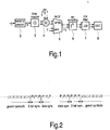
- Figure 1 shows a simplified circuit diagram of a single slot 8PSK I/Q modulator 1, according to an aspect of the present invention.
- the modulator of Fig. 1 When the modulator of Fig. 1 is applied in a GSM system, the speech signal is quantized in the speech coding, and then, the quantized speech signal is organized into data frames during channel coding.
- the serial data stream is then introduced into the serial to parallel converter 2, which may be, as shown in Fig. 1 , a three-bit serial to parallel converter.
- the three-bit parallel signal is then input to a Grey Mapper 3 which maps each bit triplet on one out of eight complex signals. Then, a 3 ⁇ /8 rotation is carried for each symbol by means of complex multiplier 4. This is done to avoid zero crossings in the RF envelope.
- the output of the up-sampler 6 is input to a Finite Impulse Response (FIR) pulse-shaping filter, here referred to with CO.
- FIR Finite Impulse Response
- up sampling and FIR filtering may be merged in a more efficient polyphase interpolation filter structure.
- the output of the FIR 7 is input to a digital to analogue converter (DAC)8.
- DAC digital to analogue converter
- the MUX 5 selects between zeros during the guard period of the TDMA signal, and rotated 8PSK symbols during the active part of the burst. This is illustrated in further detail in Fig. 2 .
- Fig. 2 shows a setting of the 8PSK MUX 5 of Fig. 1 during begin and end of a burst.
- the guard symbols zeros are filled into the MUX 5.
- the rotated 8PSK symbols are inserted into the MUX 5.
- the 8PSK symbol is maintained at the MUX 5 until the end of the three tail symbols. With the beginning of the following guard symbols, zeros are inserted into the MUX 5.
- Feeding the up-sampler/filter with zeros has the following effect: the leading zeros enable a smooth step-on response of the filter when it is excited by the early rotated 8PSK symbols.
- the trailing zeros filling the late rotated 8 PSK symbols enable a smooth step-off response.
- Fig. 3 shows an exemplary embodiment of a single slot quadratic GMSK I/Q modulator 9, according to an aspect of the present invention.
- Fig. 3 is a simplified circuit diagram.
- GMSK is a non-linear modulation scheme with pulse-shaping in the phase domain in contrast to linear modulation schemes with pulse shaping in the I/Q domain.
- P. Jung's "Laurent's decomposition of Binary Digital Continuous Phase Modulated Signals with Modulation Index 1/2 Revisited" IEEE transactions on communications, vol. 42, No. 2/3/4, 1994 , one may implement a GMSK modulator by superimposing a series of linearly modulated signals.
- the corresponding shaping filters are denoted as C0, C1, ...Cn.
- the input of the FIR filter C0 14 is generated as follows: the GMSK bits are inserted into a mapper 10.
- the output signal of the mapper 10 is input to a digital multiplier 11, which multiplies the output signals of the mapper 10 with a complex phasor e jk ⁇ /2 .
- the multiplied signals are provided to a MUX 12 which output signals are provided to an up-sampler 13, corresponding to the up-sampler 6 in Fig. 1 .
- the output signal of the up-sampler 13 is input to the FIR filter C0 14 which output signal is added to the output signal of FIR filter C1 21 and supplied to the DAC 15.
- the DAC 15 corresponds to the DAC 8 of Fig. 1 .
- the input of the FIR filter C1 21 is obtained from the modulating bits by applying a Finite State Machine (FSM) 16, a mapper 17 and a multiplication by means of a digital multiplier 18 with a complex phasor e j(k-1) ⁇ /2 .
- the output signal of the digital multiplier 18 is input into the MUX 19 which output signal is provided to the up-sampler 20.
- the output signal of the up-sampler 20 is provided to the FIR filter C1 21.
- the up-sampler 20 corresponds to the up-sampler 6 of Fig. 1 .
- the input of a shaping filter Cn is obtained from the modulating bits by applying a FSM, a mapper and a multiplication with a complex phasor e jk ⁇ /2 .
- the C0 filter is adopted as the shaping filter for 8PSK to obtain a power spectral density (PSD) which is similar to the PSD of the GMSK.
- PSD power spectral density
- the quadratic GMSK modulator as shown in Fig. 3 has the advantage that the pulse-shaping filters may be applied for envelope shaping in the same way as described with reference to the 8PSK modulator depicted in Fig. 1 . This will be described further with reference to Fig. 4 .
- Figure 4 shows an exemplary setting of the MUXs 12 and 19 of Fig. 3 during begin and an end of a time slot or burst.
- the left-hand side of Fig. 4 shows the setting during begin of a time slot and the right-hand side of Fig. 4 shows the setting at the end of a time slot.
- zeros are inserted by the MUXs 12 and 19 during all guard bits except the last guard bit of the leading guard interval and the first guard bit of the trailing guard interval.
- the GMSK signals are supplied to the u-samplers 13 and 20. This setting of the innermost and outmost guard symbols to the GMSK signals is compulsory for GMSK, because the phase error in the region of the outermost tail bits would otherwise increase too much.
- the modulator of Figure 3 with a setting of MUXs 12 and 19 as shown in Fig. 4 allows for smooth edges of the TX envelope.
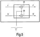
- Figure 5 shows a simplified sketch of a digital I/Q modulator 22, comprising digital multipliers 23.
- I/Q signals are provided to the digital multipliers 23 which multiply each I signal and each Q signal with a dip-shaped waveform generating digital signals I' Q' having a dip in the envelope.
- the digital multipliers 23 introduce the dips in the envelope of the digital I/Q signal in the guard interval of subsequent time slots.
- the digital I/Q modulator may be a 8PSK modulator 1, as shown in Fig. 1 , a GMSK modulator 9, as shown in Fig. 3 , or a combination of both modulators 1 and 9, or parts thereof.
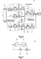
- Fig. 6 shows a multislot 8PSK/GMSK I/Q modulator 24, according to an exemplary embodiment of the present invention.
- the modulator 24 of Fig. 6 is a combination of the 8PSK modulator 1 of Fig. 1 and the quadratic GMSK modulator 9 of Fig. 3 .
- the modulator 24 of Fig. 6 comprises an 8PSK modulator comprising the three- bit serial to parallel converter 2, the grey mapper 3, the complex multiplier 4, a multiplexer 26 referred to as C0 MUX which will be described in the following, an up-sampler 6 and a FIR filter C0 7.
- a linear branch of the GMSK modulator comprises the mapper 10, the complex multiplier 11, the C0 MUX 26, the up-sampler 6 corresponding to the up-sampler 13 of Fig. 3 and the FIR filter C0 7 corresponding to the FIR filter C0 14 of Fig. 1 .
- a quadric branch of the GMSK modulator comprises the FSM 16, the mapper 17, the complex multiplier 18, the GMSK MUX 19, now referred to as C1 MUX, the up-sampler 20 and FIR filter C1 21. Furthermore, the modulator 24 of Fig.
- the 6 has a multiplexer 25 which provides the serial data stream to be modulated with the 8PSK modulation scheme to the serial to parallel converter 2, and which provides the serial data stream to be modulated with the GMSK modulation scheme to the mapper 10 and the FSM 16.
- the output signal of the FIR filter C0 is provided directly to the DAC 8.
- the output of the FIR filter C0 7 and of the FIR filter C1 21 are added and applied to the DAC 8.
- the multiplexers C0 MUX 26, C1 MUX 19 and multiplexer 25 enable the two-mode operation of the modulator: the 8PSK mode and the GMSK mode. Furthermore, these multiplexers enable configuration of the modulator as 8PSK modulator, GMSK modulator or linearized GMSK modulator.
- Fig. 7 shows the Finite State Machine 16 and the quadratic branch of the GMSK modulator with more detail.
- the FSM 16 comprises a first register 30 and a second register 31 and a first modulo 2 adder 32 and a second modulo 2 adder 33.
- the input of the FSM 16 is provided to the first register 30 and to the modulo 2 adder 32.
- the output of the first register 30 is provided to the second register 31 and to the first modulo 2 adder.
- the outputs of the second registers 31 and the first modulo 2 adder 32 are provided to the second modulo 2 adder 33 and then output to the mapper 17.
- FIG. 8 A sequence of the C0 MUX 26 and C1 MUX 19 settings during the transition from an 8PSK burst to a GMSK burst is depicted in Fig. 8 .
- Fig. 8 shows an exemplary setting of C0 MUX 26 and C1 MUX 19 during the transition from an 8 PSK time slot and a GMSK time slot and vice versa.
- the C0 MUX 26 provides in the 8PSK mode the 8PSK signal to the up-sampler 6 throughout the data signal and the three tail symbols. Then, during the first seven guard symbols, the C0 MUX 26 provides zeros to the up-sampler 6. During the last guard symbol, the C0 MUX 26 provides the GMSK signal of the linear branch of the GMSK modulator to the up-sampler 6. Then, during the three tail symbols and the following data symbols, the C0 MUX 26 provides the GMSK signal of the linear branch of the GMSK modulator, i.e. the signal output by the complex multiplier 11 to the up-sampler 6.
- the C1 MUX 19 provides zeros to the up-sampler 20 during the data symbol, where the 8 PSK signal is provided to the DAC 8, during the three tail symbols, while the 8PSK signal is provided to the DAC 8 during the first seven bits of the eight guard symbols. Then, when the signal is switched to the GMSK signal, the C1 MUX 19 provides the GMSK signal of the quadratic branch of the GMSK modulator, i.e. the output of the complex multiplier 18 to the up-sampler 20 during the last, i.e. the eighth bit of the eight guard symbols of the guard interval. Then, during the three tail symbols and the data symbols, the output of the complex multiplier 18 is provided to the up-sampler 20.
- the C0 MUX 26 In case it is switched from a time slot to which the GMSK modulation scheme is applied to a subsequent time slot applying the 8PSK modulation scheme, the C0 MUX 26 provides the output signal of the complex multiplier 11 to the up-sampler 6 during the data symbols, during the three tails symbols and during the first symbol of the eight guard symbols. Then, the C0 MUX 26 provides seven zeros during the remaining seven guard symbols to the up-sampler 6. With the start of the subsequent three tail symbols of the subsequent time-slot with the 8PSK modulation scheme, the C0 MUX 26 provides the output signal of the complex multiplier 4 to the up-sampler 6 during the tail symbols and the data symbols.
- the C1 MUX 19 When a switching from the GMSK modulation scheme to the 8PSK modulation scheme is performed for subsequent time slots, the C1 MUX 19 provides the output signal of the complex multiplier 18 to the up-sampler 20 during the data symbols during the three tail symbols and during the first one of the eight guard symbols. Then, for the remaining seven bits of the guard symbol, for the following tail symbol and following data symbol where the 8PSK is performed, the C1 MUX 19 provides zeros to the up-sampler 20.
- Fig. 9 shows an example of a hypothetical multi-slot TX envelope p tx and the corresponding power p n which can be observed in an adjacent channel when a switching is performed from 8PSK in one slot to GMSK in the following slot.
- the average power in the 8PSK TS is assumed higher than the average power in the GMSK TS.
- a dip in the envelope p tx between the 8PSk modulation scheme in the first slot and the GMSK modulation scheme in the second slot there is, according to an exemplary embodiment of the present invention, a dip.
- This dip is inserted, as explained in detail above, by either multiplying both I and Q signals with the dip-shaped waveform or by provoking a step-off response followed by a step-on response of the pulse-shaping filter, by filling the pulse-shaping filters with zeros.
- Fig. 9 shows a relatively small dip
- the size of the dip may be varied, in accordance with the requirements in the respective system.
- the smooth dip in the TX envelope results in a transition in the adjacent channel power without showing a distinct peak. The dip is not resolved because it lasts shorter than the time constant of the resolution filter.
- the effect of the dip is to avoid steps in the I/Q signal due to switching the modulation scheme and to hide steps in the TX envelope due to switching of the power levels in subsequent time slots.
- the introduction of the dip in the envelope allows to minimize interference in adjacent channels.
- the two multiplexers C0 MUX 26 and C1 MUX 19 serve for feeding complex value zeros rather than the complex value symbols into the up-samplers 6 and 20 which proceed the pulse-shaping filters FIR C0 7 and FIR C1 21.
- the modulator 24 as shown in Fig. 6 allows the use of a linear power amplifier, while avoiding interferences between adjacent channels. Also, a simple discrete gain VGA may be employed rather than a continuous gain VGA. Since the signal processing according to the present invention is carried out in the digital domain, no problems with tolerances of analogue circuits are encountered. Also, a generation of an analogue control voltage for a continuous VGA is made obsolete.
- the dip-shaping is for free, since the filters and up-samplers are required anyway.
- the modulator 24 allows a simple control of the modulation and the double use of the FIR filter C 07 for the linear branch of the GMSK modulator and the 8PSK modulator.
- a modulator such as modulator 24 may preferably be used, for example, in GSM-, EDGE- or in EGPRS chipsets.
- the retarding timing elements of the FIR filters which are filled during regular operation sequentially, may be filled also with preferably initial values in parallel.
- This allows for additional freedom in the design of the transitions between time slots.
- it may be preferable to abruptly insert a GMSK modulated signal having a constant envelope at the beginning of the guard period after the smooth down ramping of a 8 PSK time slot.
- this may also be achieved by a parallel loading of suitable initial values.
Landscapes
- Engineering & Computer Science (AREA)
- Signal Processing (AREA)
- Computer Networks & Wireless Communication (AREA)
- Physics & Mathematics (AREA)
- Nonlinear Science (AREA)
- Digital Transmission Methods That Use Modulated Carrier Waves (AREA)
- Time-Division Multiplex Systems (AREA)
Description
- The present invention relates to a modulator for generating a digital I/Q signal having a plurality of time-slots, to a signal processing method for generating a digital I/Q signal having a plurality of time-slots and to a computer program for a time division multiple access (TDMA) transmitter for a global system for mobile communications (GSM), enhanced data rates for GSM evolution (EDGE) or enhanced general packet radio service (EGPRS) system.
- In 1997, a suggestion for EDGE was filed at the European Standardization Institute, ETSI. The standardization of EDGE will be carried out in two phases. A part of the first phase specifies EGPRS, which is an extension of the existing GPRS. EGPRS introduces the 8PSK (phase shift keying) modulation scheme, which has the potential for higher data rate than the established GMSK (Gaussian minimum shift keying) modulation scheme. This new 8PSK modulation scheme has more stringent requirements with respect to the linearity of the power amplifier in the TX (transmission) chain since, in contrast to GMSK, the amplitude is not constant. Therefore, while the constant envelope of the GMSK enabled the employment of a saturated power amplifier (PA), which is more power efficient than a linear PA, the variable envelope of the 8PSK modulation scheme demands for a linear PA.
- When the 8PSK modulation scheme is employed in multi-time slot (TS) operation. It is required to adjust the TX power for every TS individually as demanded by the BSC. The TX power transient between the TSs should be smooth. Otherwise, if the TX power transient between the TSs is not smooth, interferences may occur with other users on adjacent channels. Due to this, it is normally not possible to simply switch the gain of the TX path abruptly. In addition to that, the gain of the TX path is usually varied in the analogue domain. Due to this, a continuous variable gain amplifier (VGA) is required in the TX chain, for adjusting the TX power level. Such a VGA is controlled by an appropriately shaped analogue control voltage. The provision of a VGA and the generation of the appropriately shaped analogue control voltage are expensive. In addition to that, such an arrangement is prone to defects, which are inherent to such an analogue circuitry. In addition to that, such an analogue circuitry has tolerances which, as known to the person skilled in the art, are always trouble to deal with.
- Another problem arises in multi TS operation, when the modulation scheme in adjacent TSs is changed from 8PSK to GMSK or vice versa: such a switching between 8PSK and GMSK may provoke discontinuities in the digital I/Q signals. Such discontinuities must be avoided since they are very broadband and may cause interference on other channels.
- The requirement for smooth TX power ramping is fundamental to any multiple access system, which combines TDMA and frequency division multiple access (FDMA). Therefore, the applied standards reserve a time interval between adjacent TSs, which is dedicated to power ramping and in which no data transfer occurs. According to the GSM standard, this time interval is denoted as "guard interval".
- The introduction of GPRS led to the extension of the first method towards multi time slot operation. Here, the power ramping voltage has a step shape with smooth edges. VANKKA J ET AL: "A GSM/EDGE/WCDMA modulator with on-chip D/A converter for base station",IEEE INTERNATIONAL SOLID-STATE CIRCUITS CONFERENCE. DIGEST OF TECHNICAL PAPERS, SAN FRANCISCO, USA, vol. 1, 5 February 2002 (2002-02-05), pages 236-463, discloses a modulator which allows power ramping on a time-slot basis. It is an object of the present invention to minimize interferences between adjacent time slots.
- According to an exemplary embodiment of the present invention, this object is solved with a modulator for generating a digital I/Q signal having a plurality of time slots, the modulator comprising means for introducing a dip in an envelope of the digital I/Q signal in a guard interval between adjacent time slots of the plurality of time slots.
- Such modulator according to an exemplary embodiment of the present invention as set forth in
claim 1 allows the use of a linear power amplifier in the digital I/Q modulator supporting multi time slot operation of wireless TDMA transmitters. In other words, the difficulties, which are encountered in a linear transmitter for EGPRS, may be overcome by introducing dips in the envelope of the digital or I/Q signal during the guard interval between adjacent time slots. Furthermore, the introduction of dips in the envelope of the digital or I/Q signal may have the effect that unwanted abrupt switching transients in the TX signal due to abrupt switching of the gain of the TX path can be avoided. This can be done by switching the gain of the TX path during the dip in the I/Q signal when the TX signal is down. Accordingly, interference between adjacent channels occurring with a change of the TX power level between adjacent time slots is minimized. - Furthermore, with the introduction of dips in the envelope of the digital I/Q signal during the guard interval between adjacent time slots, unwanted discontinuities in the I/Q signal when switching between the 8PSK and the GMSK modulation scheme may be avoided. Accordingly, interferences in adjacent channels occurring when switching between 8PSK and GMSK may be minimized.
- Furthermore, a discrete gain VGA rather than a continuous gain VGA may be employed in the modulator. Also, since the dips are introduced in the digital domain, there is no trouble with tolerances of analogue circuitry. In addition to that, the present invention makes a generation of the analogue control voltage for the continuous VGA obsolete.
- According to yet another exemplary embodiment of the present invention as set forth in
claim 8, a signal processing method for generating a digital I/Q signal in a modulator is provided. According to the present invention, there is also provided a computer program as set forth inclaim 11. As apparent from the above, a digital I/Q modulator is suggested which efficiently supports multi-time slot operation of wireless TDMA transmitters employing a linear power amplifier. It is an aspect of the present invention to introduce dips in the envelope of the digital I/Q signal in the guard interval between adjacent time slots. These dips avoid interference on adjacent radio frequency channels when the gain of the TX chain is switched abruptly, in order to change the power of the TX signal. In addition, a signal processing topology is suggested for generating the dips which is in particular attractive if the modulation scheme in adjacent time slots changes from GMSK to 8 PSK, or vice versa. - These and other aspects of the present invention will be apparent from and elucidated with reference to the embodiments described hereinafter. These embodiments will be described with reference to the following Figures:
-
Fig. 1 shows a single slot 8PSK I/Q modulator according to an aspect of the present invention. -
Fig. 2 shows a setting of the 8PSK MUX of the modulator ofFig. 1 during begin and at the end of a burst according to an aspect of the present invention. -
Fig. 3 shows a single slot quadratic GMSK I/Q modulator according to an aspect of the present invention. -
Fig. 4 shows a setting of the GMSK multiplexer in the modulator ofFig. 3 during begin and end of a time slot according to an aspect of the present invention. -
Fig. 5 shows a modulator with a digital multiplier for multiplying the digital I/Q signals with a dip-shaped waveform according to an aspect of the present invention. -
Fig. 6 shows a multi-slot 8PSK/GMSK I/Q modulator, according to an aspect of the present invention. -
Fig. 7 shows a Finite State Machine (FSM) in the quadratic branch of the GMSK modulator ofFig. 6 , according to an aspect of the present invention. -
Fig. 8 shows a setting of the C0 MUX and the C1 MUX of the modulator ofFig. 6 during the transition between an 8PSK time slot and a GMSK time slot, and vice versa, according to an aspect of the present invention. -
Fig. 9 illustrates by means of a hypothetical multi-slot TX envelope a switching between 8PSK and GMSK at different power levels in adjacent time slots. - In the following description of the above Figures, the same reference numbers are used for the same or corresponding elements.
-
Figure 1 shows a simplified circuit diagram of a single slot 8PSK I/Q modulator 1, according to an aspect of the present invention. When the modulator ofFig. 1 is applied in a GSM system, the speech signal is quantized in the speech coding, and then, the quantized speech signal is organized into data frames during channel coding. The serial data stream is then introduced into the serial toparallel converter 2, which may be, as shown inFig. 1 , a three-bit serial to parallel converter. The three-bit parallel signal is then input to aGrey Mapper 3 which maps each bit triplet on one out of eight complex signals. Then, a 3π/8 rotation is carried for each symbol by means ofcomplex multiplier 4. This is done to avoid zero crossings in the RF envelope. After a multiplexing of the signal in the multiplexer (MUX) 5, the output of theMUX 5 is input to an up-sampler 6 by which carries out an up-sampling N=16, which inserts N-1 zeros after every input sample. The output of the up-sampler 6 is input to a Finite Impulse Response (FIR) pulse-shaping filter, here referred to with CO. In another exemplary embodiment, up sampling and FIR filtering may be merged in a more efficient polyphase interpolation filter structure. The output of theFIR 7 is input to a digital to analogue converter (DAC)8. - During operation, the
MUX 5 selects between zeros during the guard period of the TDMA signal, and rotated 8PSK symbols during the active part of the burst. This is illustrated in further detail inFig. 2 . -
Fig. 2 shows a setting of the8PSK MUX 5 ofFig. 1 during begin and end of a burst. As can be taken fromFig. 2 , during the guard symbols, zeros are filled into theMUX 5. During the leading three tail symbols, the data symbols and the trailing three tail symbols, the rotated 8PSK symbols are inserted into theMUX 5. At the end of the data symbol, the 8PSK symbol is maintained at theMUX 5 until the end of the three tail symbols. With the beginning of the following guard symbols, zeros are inserted into theMUX 5. - Feeding the up-sampler/filter with zeros has the following effect: the leading zeros enable a smooth step-on response of the filter when it is excited by the early rotated 8PSK symbols. The trailing zeros filling the late rotated 8 PSK symbols enable a smooth step-off response.
-
Fig. 3 shows an exemplary embodiment of a single slot quadratic GMSK I/Q modulator 9, according to an aspect of the present invention.Fig. 3 is a simplified circuit diagram. GMSK is a non-linear modulation scheme with pulse-shaping in the phase domain in contrast to linear modulation schemes with pulse shaping in the I/Q domain. As suggested in P. Jung's, "Laurent's decomposition of Binary Digital Continuous Phase Modulated Signals with , one may implement a GMSK modulator by superimposing a series of linearly modulated signals. The corresponding shaping filters are denoted as C0, C1, ...Cn. - The input of the
FIR filter C0 14 is generated as follows: the GMSK bits are inserted into amapper 10. The output signal of themapper 10 is input to adigital multiplier 11, which multiplies the output signals of themapper 10 with a complex phasor ejkπ/2. The multiplied signals are provided to aMUX 12 which output signals are provided to an up-sampler 13, corresponding to the up-sampler 6 inFig. 1 . The output signal of the up-sampler 13 is input to theFIR filter C0 14 which output signal is added to the output signal ofFIR filter C1 21 and supplied to theDAC 15. TheDAC 15 corresponds to theDAC 8 ofFig. 1 . - The input of the
FIR filter C1 21 is obtained from the modulating bits by applying a Finite State Machine (FSM) 16, amapper 17 and a multiplication by means of adigital multiplier 18 with a complex phasor ej(k-1)π/2. The output signal of thedigital multiplier 18 is input into theMUX 19 which output signal is provided to the up-sampler 20. The output signal of the up-sampler 20 is provided to theFIR filter C1 21. The up-sampler 20 corresponds to the up-sampler 6 ofFig. 1 . - In general, the input of a shaping filter Cn is obtained from the modulating bits by applying a FSM, a mapper and a multiplication with a complex phasor ejkπ/2. The FSM algorithm and the phase θ n of the phasor depend on the index n of the element of the series. Accordingly, as shown in
Fig. 3 , for n=0, no FSM at all is required and θ 0 = 0 applies. Since merely the 0th element of the series is used, this is denoted as linearized GMSK. Accordingly, the upper branch inFig. 3 is referred to as linear branch of the GMSK modulator. Here, it is to be noted that the C0 filter is adopted as the shaping filter for 8PSK to obtain a power spectral density (PSD) which is similar to the PSD of the GMSK. By considering the higher order elements of the series, the approximation error can be made arbitrarily small. In the practical application, it is sufficient to consider just theelements Fig. 3 is also referred to as quadratic branch of the GMSK modulator. - The quadratic GMSK modulator as shown in
Fig. 3 has the advantage that the pulse-shaping filters may be applied for envelope shaping in the same way as described with reference to the 8PSK modulator depicted inFig. 1 . This will be described further with reference toFig. 4 . -
Figure 4 shows an exemplary setting of theMUXs Fig. 3 during begin and an end of a time slot or burst. The left-hand side ofFig. 4 shows the setting during begin of a time slot and the right-hand side ofFig. 4 shows the setting at the end of a time slot. As may be taken fromFig. 4 , zeros are inserted by theMUXs - The modulator of
Figure 3 with a setting ofMUXs Fig. 4 allows for smooth edges of the TX envelope. -
Figure 5 shows a simplified sketch of a digital I/Q modulator 22, comprisingdigital multipliers 23. I/Q signals are provided to thedigital multipliers 23 which multiply each I signal and each Q signal with a dip-shaped waveform generating digital signals I' Q' having a dip in the envelope. Thedigital multipliers 23 introduce the dips in the envelope of the digital I/Q signal in the guard interval of subsequent time slots. In principle, the digital I/Q modulator may be a8PSK modulator 1, as shown inFig. 1 , aGMSK modulator 9, as shown inFig. 3 , or a combination of bothmodulators -
Fig. 6 shows a multislot 8PSK/GMSK I/Q modulator 24, according to an exemplary embodiment of the present invention. On a first glance, themodulator 24 ofFig. 6 is a combination of the8PSK modulator 1 ofFig. 1 and thequadratic GMSK modulator 9 ofFig. 3 . Themodulator 24 ofFig. 6 comprises an 8PSK modulator comprising the three- bit serial toparallel converter 2, thegrey mapper 3, thecomplex multiplier 4, amultiplexer 26 referred to as C0 MUX which will be described in the following, an up-sampler 6 and aFIR filter C0 7. A linear branch of the GMSK modulator comprises themapper 10, thecomplex multiplier 11, theC0 MUX 26, the up-sampler 6 corresponding to the up-sampler 13 ofFig. 3 and theFIR filter C0 7 corresponding to theFIR filter C0 14 ofFig. 1 . A quadric branch of the GMSK modulator, comprises theFSM 16, themapper 17, thecomplex multiplier 18, theGMSK MUX 19, now referred to as C1 MUX, the up-sampler 20 andFIR filter C1 21. Furthermore, themodulator 24 ofFig. 6 has amultiplexer 25 which provides the serial data stream to be modulated with the 8PSK modulation scheme to the serial toparallel converter 2, and which provides the serial data stream to be modulated with the GMSK modulation scheme to themapper 10 and theFSM 16. In case the 8PSK modulation scheme is applied, the output signal of the FIR filter C0 is provided directly to theDAC 8. In case the GMSK modulation scheme is applied, the output of theFIR filter C0 7 and of theFIR filter C1 21 are added and applied to theDAC 8. Themultiplexers C0 MUX 26,C1 MUX 19 andmultiplexer 25 enable the two-mode operation of the modulator: the 8PSK mode and the GMSK mode. Furthermore, these multiplexers enable configuration of the modulator as 8PSK modulator, GMSK modulator or linearized GMSK modulator. -
Fig. 7 shows theFinite State Machine 16 and the quadratic branch of the GMSK modulator with more detail. As can be taken fromFig. 7 , theFSM 16 comprises afirst register 30 and asecond register 31 and a first modulo 2adder 32 and a second modulo 2adder 33. The input of theFSM 16 is provided to thefirst register 30 and to themodulo 2adder 32. The output of thefirst register 30 is provided to thesecond register 31 and to the first modulo 2 adder. The outputs of the second registers 31 and the first modulo 2adder 32 are provided to the second modulo 2adder 33 and then output to themapper 17. - A sequence of the
C0 MUX 26 andC1 MUX 19 settings during the transition from an 8PSK burst to a GMSK burst is depicted inFig. 8 . -
Fig. 8 shows an exemplary setting ofC0 MUX 26 andC1 MUX 19 during the transition from an 8 PSK time slot and a GMSK time slot and vice versa. As may be taken fromFig. 8 , theC0 MUX 26 provides in the 8PSK mode the 8PSK signal to the up-sampler 6 throughout the data signal and the three tail symbols. Then, during the first seven guard symbols, theC0 MUX 26 provides zeros to the up-sampler 6. During the last guard symbol, theC0 MUX 26 provides the GMSK signal of the linear branch of the GMSK modulator to the up-sampler 6. Then, during the three tail symbols and the following data symbols, theC0 MUX 26 provides the GMSK signal of the linear branch of the GMSK modulator, i.e. the signal output by thecomplex multiplier 11 to the up-sampler 6. - The
C1 MUX 19 provides zeros to the up-sampler 20 during the data symbol, where the 8 PSK signal is provided to theDAC 8, during the three tail symbols, while the 8PSK signal is provided to theDAC 8 during the first seven bits of the eight guard symbols. Then, when the signal is switched to the GMSK signal, theC1 MUX 19 provides the GMSK signal of the quadratic branch of the GMSK modulator, i.e. the output of thecomplex multiplier 18 to the up-sampler 20 during the last, i.e. the eighth bit of the eight guard symbols of the guard interval. Then, during the three tail symbols and the data symbols, the output of thecomplex multiplier 18 is provided to the up-sampler 20. - In case it is switched from a time slot to which the GMSK modulation scheme is applied to a subsequent time slot applying the 8PSK modulation scheme, the
C0 MUX 26 provides the output signal of thecomplex multiplier 11 to the up-sampler 6 during the data symbols, during the three tails symbols and during the first symbol of the eight guard symbols. Then, theC0 MUX 26 provides seven zeros during the remaining seven guard symbols to the up-sampler 6. With the start of the subsequent three tail symbols of the subsequent time-slot with the 8PSK modulation scheme, theC0 MUX 26 provides the output signal of thecomplex multiplier 4 to the up-sampler 6 during the tail symbols and the data symbols. - When a switching from the GMSK modulation scheme to the 8PSK modulation scheme is performed for subsequent time slots, the
C1 MUX 19 provides the output signal of thecomplex multiplier 18 to the up-sampler 20 during the data symbols during the three tail symbols and during the first one of the eight guard symbols. Then, for the remaining seven bits of the guard symbol, for the following tail symbol and following data symbol where the 8PSK is performed, theC1 MUX 19 provides zeros to the up-sampler 20. -
Fig. 9 shows an example of a hypothetical multi-slot TX envelope ptx and the corresponding power pn which can be observed in an adjacent channel when a switching is performed from 8PSK in one slot to GMSK in the following slot. The average power in the 8PSK TS is assumed higher than the average power in the GMSK TS. As may be taken fromFig. 9 , in the envelope ptx between the 8PSk modulation scheme in the first slot and the GMSK modulation scheme in the second slot there is, according to an exemplary embodiment of the present invention, a dip. This dip is inserted, as explained in detail above, by either multiplying both I and Q signals with the dip-shaped waveform or by provoking a step-off response followed by a step-on response of the pulse-shaping filter, by filling the pulse-shaping filters with zeros. In spite of the fact thatFig. 9 shows a relatively small dip, the size of the dip may be varied, in accordance with the requirements in the respective system. As shown by the adjacent channel power pn, the smooth dip in the TX envelope results in a transition in the adjacent channel power without showing a distinct peak. The dip is not resolved because it lasts shorter than the time constant of the resolution filter. Accordingly, the effect of the dip is to avoid steps in the I/Q signal due to switching the modulation scheme and to hide steps in the TX envelope due to switching of the power levels in subsequent time slots. As shown inFig. 9 , the introduction of the dip in the envelope allows to minimize interference in adjacent channels. - As already explained in detail above, the two
multiplexers C0 MUX 26 andC1 MUX 19 serve for feeding complex value zeros rather than the complex value symbols into the up-samplers filters FIR C0 7 andFIR C1 21. As already indicated above, it is also possible to further consider higher order branches other than the 0 and the 1 branch to improve the approximation in themodulator 24, as depicted inFig. 6 . Also, as a variant, it may be possible to combine the respective up-sampler with the subsequent pulse-shaping FIR filters into an efficient polyphase interpolation filter. - Advantageously, the
modulator 24 as shown inFig. 6 allows the use of a linear power amplifier, while avoiding interferences between adjacent channels. Also, a simple discrete gain VGA may be employed rather than a continuous gain VGA. Since the signal processing according to the present invention is carried out in the digital domain, no problems with tolerances of analogue circuits are encountered. Also, a generation of an analogue control voltage for a continuous VGA is made obsolete. - Due to the employment of the
multiplexers C MUX 26 andC MUX 19 in themodulator 24 ofFig. 6 , the dip-shaping is for free, since the filters and up-samplers are required anyway. Also themodulator 24 allows a simple control of the modulation and the double use of the FIR filter C 07 for the linear branch of the GMSK modulator and the 8PSK modulator. A modulator such asmodulator 24 may preferably be used, for example, in GSM-, EDGE- or in EGPRS chipsets. - According to another exemplary embodiment of the present invention, advantageously, the retarding timing elements of the FIR filters, which are filled during regular operation sequentially, may be filled also with preferably initial values in parallel. This allows for additional freedom in the design of the transitions between time slots. Thus, for example, during the application of particular transmission concepts, it may be preferable to abruptly insert a GMSK modulated signal having a constant envelope at the beginning of the guard period after the smooth down ramping of a 8 PSK time slot. According to an exemplary aspect of the present invention, advantageously, this may also be achieved by a parallel loading of suitable initial values.
Claims (11)
- A Modulator (9) for generating a digital I/Q signal having a plurality of timeslots, the modulator including means (12,19) for introducing a dip in an envelope of the digital I/Q signal in a guard interval between adjacent time-slots of the plurality of time-slots,
characterized in that
the modulator further includes a first branch (10-14) of a first order equal to zero with a first pulse-shaping filter (14) for providing a first linearly modulated signal in the I/Q domain, at least one second branch (16-21) of a second order higher than zero with a second pulse-shaping filter (21) for providing a second linearly modulated signal in the I/Q domain, and an adder for adding the first linearly modulated signal and the second linearly modulated signal to approximate a GMSK modulator, the means for introducing the dip including means (12,19) for filling digital zeros into the first pulse-shaping filter and the second pulse-shaping filter. - The modulator (9) according to claim 1, wherein the first branch (10-14) includes a first mapper (10) for receiving GMSK bits, a first digital multiplier (11) for multiplying an output of the first mapper by a first complex phasor corresponding to the first order, a first multiplexer (12) for feeding digital zeros or an output of the first digital multiplier, a first up-sampler (13) for inserting zeros into an output of the first multiplexer and for providing an output thereof to the first pulse-shaping filter (14), and wherein the second branch (16-21) includes a finite state machine (16) for receiving the GMSK bits, a second mapper (17) for receiving an output of the finite state machine, a second digital multiplier (18) for multiplying an output of the second mapper by a second complex phasor corresponding to the second order, a second multiplexer (19) for feeding digital zeros or an output of the second digital multiplier, a second up-sampler (20) for inserting zeros into an output of the second multiplexer and for providing an output thereof to the second pulse-shaping filter (21).
- The modulator (9) according to claim 1 or 2, wherein the guard interval is formed by a plurality of guard bits, the means (12,19) for filling digital zeros including means (12,19) for filling digital zeros into the first pulse-shaping filter (14) and the second pulse-shaping filter (21) during all the guard bits except a first guard bit and a last guard bit.
- The modulator (24) according to any claim from 1 to 3, further including an 8PSK modulator (2-4,26,6,7), the 8PSK modulator and the GMSK modulator (1,11,6,7,16-21) sharing the first pulse-shaping filter (7).
- The modulator (24) according to claim 4, wherein the guard interval is formed by a plurality of guard bits, the means (19,26) for filling digital zeros including means (19,26) for filling digital zeros into the first pulse-shaping filter (7) and the second pulse-shaping filter during all the guard bits except a first guard bit during a switching from a time slot in a GMSK mode of operation to a time slot in a 8PSK mode, and filling digital zeros into the first pulse-shaping filter and the second pulse-shaping filter during all the guard bits except a last guard bit during a switching from a time slot in the 8PSK mode to a time slot in the GMSK mode.
- The modulator (24) according to claim 4 or 5 when dependent directly or indirectly on claim 2, wherein the 8PSK modulator (2-4,26,6,7) includes a serial to parallel converter (2) for receiving a serial data stream, a grey mapper (3) for mapping an output of the serial to parallel converter into a complex signal, a further digital multiplier (4) for multiplying an output of the grey mapper by a further complex phasor, said first multiplexer (26) for feeding digital zeros, the output of the first digital multiplier (11) or an output of the further digital multiplier, said first up-sampler (6) for inserting zeros into the output of the first multiplexer and for providing an output thereof to said first pulse-shaping filter (7), and wherein the modulator includes a further multiplexer (25) for selecting the 8PSK modulator or the GMSK modulator.
- A transmitter including a modulator (9;24) according to any claim from 1 to 6.
- A signal processing method for generating a digital I/Q signal having a plurality of time-slots in a modulator (9), the signal processing method including the steps of:introducing a dip in an envelope of the digital I/Q signal in a guard interval between adjacent time-slots of the plurality of time-slots,characterized byproviding a first linearly modulated signal in the I/Q domain by means of a first branch (10-14) of a first order equal to zero with a first pulse-shaping filter (14),providing a second linearly modulated signal in the I/Q domain by means of at least one second branch (16-21) of a second order higher than zero with a second pulse-shaping filter (21), andadding the first linearly modulated signal and the second linearly modulated signal to approximate a GMSK modulator, the step of introducing the dip including filling digital zeros into the first pulse-shaping filter and the second pulse-shaping filter.
- The method according to claim 8, wherein the guard interval is formed by a plurality of guard bits, the step of filling digital zeros including:filling digital zeros into the first pulse-shaping filter (14) and the second pulse-shaping filter (21) during all the guard bits except a first guard bit and a last guard bit.
- The method according to claim 8 or 9, wherein the modulator (24) further includes an 8PSK modulator (2-4,26,6,7), the 8PSK modulator and the GMSK modulator (1,11,6,7,16-21) sharing the first pulse-shaping filter (7), and wherein the guard interval is formed by a plurality of guard bits, the step of filling digital zeros including:filling digital zeros into the first pulse-shaping filter (7) and the second pulse-shaping filter during all the guard bits except a first guard bit during a switching from a time slot in a GMSK mode of operation to a time slot in the 8PSK mode, and filling digital zeros into the first pulse-shaping filter and the second pulse-shaping filter during all the guard bits except a last guard bit during a switching from a time slot in the 8PSK mode to a time slot in the GMSK mode.
- A computer program including code means for causing a modulator (9;24) to perform the steps of the method according to any claim from 8 to 10.
Priority Applications (1)
| Application Number | Priority Date | Filing Date | Title |
|---|---|---|---|
| EP03791136.9A EP1537709B1 (en) | 2002-08-28 | 2003-08-14 | Method for generating a digital i/q signal in a tdma transmitter and corresponding modulator |
Applications Claiming Priority (4)
| Application Number | Priority Date | Filing Date | Title |
|---|---|---|---|
| EP02102229 | 2002-08-28 | ||
| EP02102229 | 2002-08-28 | ||
| PCT/IB2003/003768 WO2004021659A1 (en) | 2002-08-28 | 2003-08-14 | Method for generating i/q signal in a tdma transmitter and corresponding modulator |
| EP03791136.9A EP1537709B1 (en) | 2002-08-28 | 2003-08-14 | Method for generating a digital i/q signal in a tdma transmitter and corresponding modulator |
Publications (2)
| Publication Number | Publication Date |
|---|---|
| EP1537709A1 EP1537709A1 (en) | 2005-06-08 |
| EP1537709B1 true EP1537709B1 (en) | 2018-02-14 |
Family
ID=31970438
Family Applications (1)
| Application Number | Title | Priority Date | Filing Date |
|---|---|---|---|
| EP03791136.9A Expired - Lifetime EP1537709B1 (en) | 2002-08-28 | 2003-08-14 | Method for generating a digital i/q signal in a tdma transmitter and corresponding modulator |
Country Status (6)
| Country | Link |
|---|---|
| US (1) | US7680210B2 (en) |
| EP (1) | EP1537709B1 (en) |
| JP (1) | JP2005537743A (en) |
| CN (1) | CN1679290B (en) |
| AU (1) | AU2003255985A1 (en) |
| WO (1) | WO2004021659A1 (en) |
Families Citing this family (36)
| Publication number | Priority date | Publication date | Assignee | Title |
|---|---|---|---|---|
| US7394844B1 (en) * | 2003-05-19 | 2008-07-01 | Xtendwave, Inc. | Code division multiple access employing orthogonal filter banks |
| US7515652B2 (en) * | 2003-09-30 | 2009-04-07 | Broadcom Corporation | Digital modulator for a GSM/GPRS/EDGE wireless polar RF transmitter |
| EP1692834A1 (en) | 2003-12-04 | 2006-08-23 | Koninklijke Philips Electronics N.V. | Avoidance of discontinuities when switching between modulation schemes |
| WO2005088922A1 (en) * | 2004-03-04 | 2005-09-22 | Qualcomm Incorporated | A method of and an apparatus for effecting a smooth transition between adjacent symbol bursts transmitted in different modulation formats |
| KR100853076B1 (en) | 2004-06-24 | 2008-08-19 | 콸콤 인코포레이티드 | Unified modulator for continuous phase modulation and phase-shift keying |
| US8009761B2 (en) * | 2004-06-24 | 2011-08-30 | Qualcomm Incorporation | Unified modulator for continuous phase modulation and phase-shift keying |
| CN101431353B (en) * | 2004-07-09 | 2012-12-26 | 联发科技股份有限公司 | Control method and apparatus for delivering power amplifier |
| US7991076B2 (en) * | 2004-07-29 | 2011-08-02 | St-Ericsson Sa | Complex signal scaling for phase and/or amplitude modulated signals |
| CN1993951B (en) | 2004-07-29 | 2010-08-11 | Nxp股份有限公司 | Enhanced bit mapping for digital interface of a wireless communication equipment in multi-time slot and multi-mode operation |
| ATE415039T1 (en) * | 2004-07-29 | 2008-12-15 | Nxp Bv | MODULATOR WITH INSTANT MODULATION SCHEME CHANGE IN MULTI-TIME SLOT AND MULTI-MODE OPERATION FOR A WIRELESS COMMUNICATIONS DEVICE |
| FR2878393B1 (en) * | 2004-11-23 | 2007-01-12 | Commissariat Energie Atomique | METHOD AND DEVICE FOR COMPENSATING FOR IMBALANCES OF A RECEIVER |
| US7362820B2 (en) * | 2005-05-18 | 2008-04-22 | Motorola, Inc. | Apparatus and method for modulating and digitally predistorting a signal in a multiple modulation schemes |
| US7545881B2 (en) * | 2005-05-23 | 2009-06-09 | Qualcomm Incorporated | Method and apparatus for controlling spurious transmissions in a communications system |
| JP2008547363A (en) * | 2005-07-04 | 2008-12-25 | フリースケール セミコンダクター インコーポレイテッド | Ramping with a primed FIR filter in a multimode transmitter |
| US20070025468A1 (en) * | 2005-07-28 | 2007-02-01 | Weidong Li | GMSK/8-PSK mix-mode support for GSM/GPRS/EDGE compliant handsets |
| JP2008005402A (en) * | 2005-08-25 | 2008-01-10 | Yokogawa Electric Corp | Testing device |
| US7697901B2 (en) | 2005-09-26 | 2010-04-13 | St-Ericsson Sa | Digital variable gain mixer |
| US20070072652A1 (en) * | 2005-09-26 | 2007-03-29 | Sheng-Ming Shan | Controlling power output of a transceiver |
| US7720176B2 (en) | 2005-09-26 | 2010-05-18 | St-Ericsson Sa | Edge transceiver architecture and related methods |
| KR100786101B1 (en) * | 2005-12-22 | 2007-12-21 | 엘지전자 주식회사 | signal transmitting method |
| US8208877B2 (en) | 2007-03-21 | 2012-06-26 | Intel Corporation | Digital modulator and method for initiating ramp power transitions in a mobile handset transmitter |
| GB0808886D0 (en) * | 2008-05-15 | 2008-06-25 | Cambridge Silicon Radio Ltd | Dual purpose modulator |
| KR101289889B1 (en) * | 2009-11-23 | 2013-07-24 | 한국전자통신연구원 | Transmiiting device, receiving device, transmitting method and receiving method for wireless communication system |
| US8537041B2 (en) | 2011-05-12 | 2013-09-17 | Andrew Llc | Interpolation-based digital pre-distortion architecture |
| EP2957081A1 (en) * | 2013-02-12 | 2015-12-23 | Nokia Solutions and Networks Oy | Zero insertion for isi free ofdm reception |
| EP2985966B1 (en) * | 2013-04-12 | 2017-06-07 | Sun Patent Trust | Transmission apparatus |
| JP2016167781A (en) * | 2015-03-10 | 2016-09-15 | 富士通株式会社 | Radio communication device and method of controlling radio communication device |
| JP6755298B2 (en) * | 2015-07-06 | 2020-09-16 | テレフオンアクチーボラゲット エルエム エリクソン(パブル) | Resource allocation for data transmission in wireless systems |
| US10069666B2 (en) * | 2015-07-20 | 2018-09-04 | Telefonaktiebolaget Lm Ericsson (Publ) | Transceiver architecture that maintains legacy timing by inserting and removing cyclic prefix at legacy sampling rate |
| CN106936758B (en) * | 2015-12-29 | 2019-12-13 | 联芯科技有限公司 | Method and device for improving radio frequency index of EDGE transmitter |
| US10439851B2 (en) * | 2016-09-20 | 2019-10-08 | Ohio State Innovation Foundation | Frequency-independent receiver and beamforming technique |
| US10541721B2 (en) * | 2017-09-26 | 2020-01-21 | Analog Devices Global Unlimited Company | Modulation index adjustment |
| US11522600B1 (en) | 2018-08-01 | 2022-12-06 | Cohere Technologies, Inc. | Airborne RF-head system |
| CN111200571B (en) * | 2018-11-19 | 2021-10-01 | 华为技术有限公司 | Signal transmission method and device |
| US10797920B1 (en) * | 2020-03-18 | 2020-10-06 | Rockwell Collins, Inc. | High-entropy continuous phase modulation data transmitter |
| CN112104582B (en) * | 2020-11-09 | 2021-02-05 | 电子科技大学 | I/Q domain modulation method, double domain modulation method and multiple access communication method |
Family Cites Families (15)
| Publication number | Priority date | Publication date | Assignee | Title |
|---|---|---|---|---|
| US3676478A (en) * | 1968-12-04 | 1972-07-11 | Bayer Ag | Silyl-substituted urea derivatives |
| US3971751A (en) * | 1975-06-09 | 1976-07-27 | Kanegafuchi Kagaku Kogyo Kabushiki Kaisha | Vulcanizable silylether terminated polymer |
| US4644561A (en) * | 1985-03-20 | 1987-02-17 | International Mobile Machines Corp. | Modem for RF subscriber telephone system |
| DE3636974A1 (en) * | 1986-10-30 | 1988-05-05 | Bayer Ag | POLY- (ETHER-URETHANE UREA) POLYADDITION PRODUCTS, THEIR PRODUCTION, MIXTURE CONTAINING THESE AND THEIR USE AS IMPRESSION MATERIALS |
| DE4029505A1 (en) * | 1990-09-18 | 1992-03-19 | Henkel Kgaa | MOISTURIZING, ALKOXYSILANE-TERMINATED POLYURETHANE |
| US5590755A (en) * | 1993-05-05 | 1997-01-07 | Maryland Wire Belts, Inc. | Woven-wire belt with vertically-oriented lateral edges and conveyance methods and apparatus |
| JP3344004B2 (en) | 1993-06-30 | 2002-11-11 | カシオ計算機株式会社 | Digital modulator |
| JP3454623B2 (en) | 1995-11-28 | 2003-10-06 | 三洋電機株式会社 | π / 4 shift QPSK quadrature modulator |
| US5852630A (en) * | 1997-07-17 | 1998-12-22 | Globespan Semiconductor, Inc. | Method and apparatus for a RADSL transceiver warm start activation procedure with precoding |
| JP3570898B2 (en) * | 1998-08-24 | 2004-09-29 | 日本電気株式会社 | Pre-distortion circuit |
| US6438115B1 (en) * | 1999-03-08 | 2002-08-20 | Telefonaktiebolaget L M Ericsson (Publ) | High speed data communication system and method |
| US7012977B2 (en) * | 2000-12-29 | 2006-03-14 | Telefonaktiebolaget Lm Ericsson (Publ) | System, method and apparatus for wireless channel parameter estimation in spread spectrum communication systems |
| US6865235B2 (en) * | 2001-03-06 | 2005-03-08 | Agere Systems Inc. | Multi-protocol modulator |
| US7158494B2 (en) * | 2001-10-22 | 2007-01-02 | Matsushita Electric Industrial Co., Ltd. | Multi-mode communications transmitter |
| EP1341300A1 (en) * | 2002-02-27 | 2003-09-03 | Lucent Technologies Inc. | Power amplifier with an adjustable quiescent current |
-
2003
- 2003-08-14 CN CN038204363A patent/CN1679290B/en not_active Expired - Fee Related
- 2003-08-14 AU AU2003255985A patent/AU2003255985A1/en not_active Abandoned
- 2003-08-14 EP EP03791136.9A patent/EP1537709B1/en not_active Expired - Lifetime
- 2003-08-14 US US10/525,473 patent/US7680210B2/en not_active Expired - Fee Related
- 2003-08-14 JP JP2004532422A patent/JP2005537743A/en active Pending
- 2003-08-14 WO PCT/IB2003/003768 patent/WO2004021659A1/en active Application Filing
Also Published As
| Publication number | Publication date |
|---|---|
| AU2003255985A1 (en) | 2004-03-19 |
| JP2005537743A (en) | 2005-12-08 |
| CN1679290B (en) | 2010-06-02 |
| CN1679290A (en) | 2005-10-05 |
| US20050249312A1 (en) | 2005-11-10 |
| WO2004021659A1 (en) | 2004-03-11 |
| US7680210B2 (en) | 2010-03-16 |
| EP1537709A1 (en) | 2005-06-08 |
Similar Documents
| Publication | Publication Date | Title |
|---|---|---|
| EP1537709B1 (en) | Method for generating a digital i/q signal in a tdma transmitter and corresponding modulator | |
| US7158494B2 (en) | Multi-mode communications transmitter | |
| US8009761B2 (en) | Unified modulator for continuous phase modulation and phase-shift keying | |
| JP4448168B2 (en) | Method and apparatus for achieving a smooth transition between adjacent symbol bursts transmitted in different modulation formats | |
| US6611565B1 (en) | Broadband transmitter for a signal consisting of a plurality of digitally modulated carriers | |
| US8102937B2 (en) | Enhanced bit mapping for digital interface of a wireless communication equipment in multi-time slot and multi-mode operation | |
| US7158578B2 (en) | Quadrature modulator with pulse-shaping | |
| EP1776816B1 (en) | Modulator with instantaneous modulation scheme switching in multi-time slot and multi-mode operation, for a wireless communication equipment | |
| US20030174784A1 (en) | Method and system for digital modulation for burst mode applications | |
| US7974262B2 (en) | Sample acquisition timing adjustment | |
| WO2011078752A1 (en) | Data modulation | |
| US20090015344A1 (en) | Avoidance of Discontinuities When Switching Between Modulation Schemes | |
| JP2971683B2 (en) | Burst signal generator | |
| EP1071248B1 (en) | Burst shaping | |
| KR100853076B1 (en) | Unified modulator for continuous phase modulation and phase-shift keying | |
| JPH0637830A (en) | Digital modulator for brust transmission | |
| Babu et al. | GSM-EDGE modulators for 2.5 G system, an efficient parallel implementation on FPGA | |
| Vankka | 16. A GSM/EDGE/WCDMA Modulator with On-chip D/A Converter for Base Stations |
Legal Events
| Date | Code | Title | Description |
|---|---|---|---|
| PUAI | Public reference made under article 153(3) epc to a published international application that has entered the european phase |
Free format text: ORIGINAL CODE: 0009012 |
|
| 17P | Request for examination filed |
Effective date: 20050329 |
|
| AK | Designated contracting states |
Kind code of ref document: A1 Designated state(s): AT BE BG CH CY CZ DE DK EE ES FI FR GB GR HU IE IT LI LU MC NL PT RO SE SI SK TR |
|
| AX | Request for extension of the european patent |
Extension state: AL LT LV MK |
|
| DAX | Request for extension of the european patent (deleted) | ||
| RAP1 | Party data changed (applicant data changed or rights of an application transferred) |
Owner name: NXP B.V. |
|
| 17Q | First examination report despatched |
Effective date: 20091008 |
|
| GRAP | Despatch of communication of intention to grant a patent |
Free format text: ORIGINAL CODE: EPIDOSNIGR1 |
|
| INTG | Intention to grant announced |
Effective date: 20170418 |
|
| RIN1 | Information on inventor provided before grant (corrected) |
Inventor name: BAUER, H. Inventor name: BODE, P. Inventor name: DIETSCH, R. |
|
| GRAS | Grant fee paid |
Free format text: ORIGINAL CODE: EPIDOSNIGR3 |
|
| RIN1 | Information on inventor provided before grant (corrected) |
Inventor name: BAUER, HARALD Inventor name: BODE, PETER Inventor name: DIETSCH, RAINER |
|
| GRAA | (expected) grant |
Free format text: ORIGINAL CODE: 0009210 |
|
| AK | Designated contracting states |
Kind code of ref document: B1 Designated state(s): AT BE BG CH CY CZ DE DK EE ES FI FR GB GR HU IE IT LI LU MC NL PT RO SE SI SK TR |
|
| REG | Reference to a national code |
Ref country code: GB Ref legal event code: FG4D |
|
| REG | Reference to a national code |
Ref country code: CH Ref legal event code: EP |
|
| REG | Reference to a national code |
Ref country code: IE Ref legal event code: FG4D |
|
| REG | Reference to a national code |
Ref country code: DE Ref legal event code: R096 Ref document number: 60350970 Country of ref document: DE Ref country code: AT Ref legal event code: REF Ref document number: 970557 Country of ref document: AT Kind code of ref document: T Effective date: 20180315 |
|
| REG | Reference to a national code |
Ref country code: NL Ref legal event code: MP Effective date: 20180214 |
|
| REG | Reference to a national code |
Ref country code: AT Ref legal event code: MK05 Ref document number: 970557 Country of ref document: AT Kind code of ref document: T Effective date: 20180214 |
|
| PG25 | Lapsed in a contracting state [announced via postgrant information from national office to epo] |
Ref country code: CY Free format text: LAPSE BECAUSE OF FAILURE TO SUBMIT A TRANSLATION OF THE DESCRIPTION OR TO PAY THE FEE WITHIN THE PRESCRIBED TIME-LIMIT Effective date: 20180214 Ref country code: NL Free format text: LAPSE BECAUSE OF FAILURE TO SUBMIT A TRANSLATION OF THE DESCRIPTION OR TO PAY THE FEE WITHIN THE PRESCRIBED TIME-LIMIT Effective date: 20180214 Ref country code: ES Free format text: LAPSE BECAUSE OF FAILURE TO SUBMIT A TRANSLATION OF THE DESCRIPTION OR TO PAY THE FEE WITHIN THE PRESCRIBED TIME-LIMIT Effective date: 20180214 Ref country code: FI Free format text: LAPSE BECAUSE OF FAILURE TO SUBMIT A TRANSLATION OF THE DESCRIPTION OR TO PAY THE FEE WITHIN THE PRESCRIBED TIME-LIMIT Effective date: 20180214 |
|
| PG25 | Lapsed in a contracting state [announced via postgrant information from national office to epo] |
Ref country code: AT Free format text: LAPSE BECAUSE OF FAILURE TO SUBMIT A TRANSLATION OF THE DESCRIPTION OR TO PAY THE FEE WITHIN THE PRESCRIBED TIME-LIMIT Effective date: 20180214 Ref country code: SE Free format text: LAPSE BECAUSE OF FAILURE TO SUBMIT A TRANSLATION OF THE DESCRIPTION OR TO PAY THE FEE WITHIN THE PRESCRIBED TIME-LIMIT Effective date: 20180214 Ref country code: GR Free format text: LAPSE BECAUSE OF FAILURE TO SUBMIT A TRANSLATION OF THE DESCRIPTION OR TO PAY THE FEE WITHIN THE PRESCRIBED TIME-LIMIT Effective date: 20180515 Ref country code: BG Free format text: LAPSE BECAUSE OF FAILURE TO SUBMIT A TRANSLATION OF THE DESCRIPTION OR TO PAY THE FEE WITHIN THE PRESCRIBED TIME-LIMIT Effective date: 20180514 |
|
| PG25 | Lapsed in a contracting state [announced via postgrant information from national office to epo] |
Ref country code: IT Free format text: LAPSE BECAUSE OF FAILURE TO SUBMIT A TRANSLATION OF THE DESCRIPTION OR TO PAY THE FEE WITHIN THE PRESCRIBED TIME-LIMIT Effective date: 20180214 Ref country code: EE Free format text: LAPSE BECAUSE OF FAILURE TO SUBMIT A TRANSLATION OF THE DESCRIPTION OR TO PAY THE FEE WITHIN THE PRESCRIBED TIME-LIMIT Effective date: 20180214 Ref country code: RO Free format text: LAPSE BECAUSE OF FAILURE TO SUBMIT A TRANSLATION OF THE DESCRIPTION OR TO PAY THE FEE WITHIN THE PRESCRIBED TIME-LIMIT Effective date: 20180214 |
|
| REG | Reference to a national code |
Ref country code: DE Ref legal event code: R097 Ref document number: 60350970 Country of ref document: DE |
|
| PG25 | Lapsed in a contracting state [announced via postgrant information from national office to epo] |
Ref country code: SK Free format text: LAPSE BECAUSE OF FAILURE TO SUBMIT A TRANSLATION OF THE DESCRIPTION OR TO PAY THE FEE WITHIN THE PRESCRIBED TIME-LIMIT Effective date: 20180214 Ref country code: CZ Free format text: LAPSE BECAUSE OF FAILURE TO SUBMIT A TRANSLATION OF THE DESCRIPTION OR TO PAY THE FEE WITHIN THE PRESCRIBED TIME-LIMIT Effective date: 20180214 Ref country code: DK Free format text: LAPSE BECAUSE OF FAILURE TO SUBMIT A TRANSLATION OF THE DESCRIPTION OR TO PAY THE FEE WITHIN THE PRESCRIBED TIME-LIMIT Effective date: 20180214 |
|
| PLBE | No opposition filed within time limit |
Free format text: ORIGINAL CODE: 0009261 |
|
| STAA | Information on the status of an ep patent application or granted ep patent |
Free format text: STATUS: NO OPPOSITION FILED WITHIN TIME LIMIT |
|
| 26N | No opposition filed |
Effective date: 20181115 |
|
| PG25 | Lapsed in a contracting state [announced via postgrant information from national office to epo] |
Ref country code: SI Free format text: LAPSE BECAUSE OF FAILURE TO SUBMIT A TRANSLATION OF THE DESCRIPTION OR TO PAY THE FEE WITHIN THE PRESCRIBED TIME-LIMIT Effective date: 20180214 |
|
| REG | Reference to a national code |
Ref country code: DE Ref legal event code: R119 Ref document number: 60350970 Country of ref document: DE |
|
| PG25 | Lapsed in a contracting state [announced via postgrant information from national office to epo] |
Ref country code: MC Free format text: LAPSE BECAUSE OF FAILURE TO SUBMIT A TRANSLATION OF THE DESCRIPTION OR TO PAY THE FEE WITHIN THE PRESCRIBED TIME-LIMIT Effective date: 20180214 |
|
| REG | Reference to a national code |
Ref country code: CH Ref legal event code: PL |
|
| GBPC | Gb: european patent ceased through non-payment of renewal fee |
Effective date: 20180814 |
|
| PG25 | Lapsed in a contracting state [announced via postgrant information from national office to epo] |
Ref country code: CH Free format text: LAPSE BECAUSE OF NON-PAYMENT OF DUE FEES Effective date: 20180831 Ref country code: LI Free format text: LAPSE BECAUSE OF NON-PAYMENT OF DUE FEES Effective date: 20180831 Ref country code: LU Free format text: LAPSE BECAUSE OF NON-PAYMENT OF DUE FEES Effective date: 20180814 |
|
| REG | Reference to a national code |
Ref country code: BE Ref legal event code: MM Effective date: 20180831 |
|
| REG | Reference to a national code |
Ref country code: IE Ref legal event code: MM4A |
|
| PG25 | Lapsed in a contracting state [announced via postgrant information from national office to epo] |
Ref country code: DE Free format text: LAPSE BECAUSE OF NON-PAYMENT OF DUE FEES Effective date: 20190301 Ref country code: IE Free format text: LAPSE BECAUSE OF NON-PAYMENT OF DUE FEES Effective date: 20180814 |
|
| PG25 | Lapsed in a contracting state [announced via postgrant information from national office to epo] |
Ref country code: FR Free format text: LAPSE BECAUSE OF NON-PAYMENT OF DUE FEES Effective date: 20180831 Ref country code: BE Free format text: LAPSE BECAUSE OF NON-PAYMENT OF DUE FEES Effective date: 20180831 |
|
| PG25 | Lapsed in a contracting state [announced via postgrant information from national office to epo] |
Ref country code: GB Free format text: LAPSE BECAUSE OF NON-PAYMENT OF DUE FEES Effective date: 20180814 |
|
| PG25 | Lapsed in a contracting state [announced via postgrant information from national office to epo] |
Ref country code: TR Free format text: LAPSE BECAUSE OF FAILURE TO SUBMIT A TRANSLATION OF THE DESCRIPTION OR TO PAY THE FEE WITHIN THE PRESCRIBED TIME-LIMIT Effective date: 20180214 |
|
| PG25 | Lapsed in a contracting state [announced via postgrant information from national office to epo] |
Ref country code: PT Free format text: LAPSE BECAUSE OF FAILURE TO SUBMIT A TRANSLATION OF THE DESCRIPTION OR TO PAY THE FEE WITHIN THE PRESCRIBED TIME-LIMIT Effective date: 20180214 Ref country code: HU Free format text: LAPSE BECAUSE OF FAILURE TO SUBMIT A TRANSLATION OF THE DESCRIPTION OR TO PAY THE FEE WITHIN THE PRESCRIBED TIME-LIMIT; INVALID AB INITIO Effective date: 20030814 |