EP1536457A2 - Prozesskammer mit einer reflektierenden Platte - Google Patents
Prozesskammer mit einer reflektierenden Platte Download PDFInfo
- Publication number
- EP1536457A2 EP1536457A2 EP05003989A EP05003989A EP1536457A2 EP 1536457 A2 EP1536457 A2 EP 1536457A2 EP 05003989 A EP05003989 A EP 05003989A EP 05003989 A EP05003989 A EP 05003989A EP 1536457 A2 EP1536457 A2 EP 1536457A2
- Authority
- EP
- European Patent Office
- Prior art keywords
- assembly
- lid
- insulator
- base plate
- reflective
- Prior art date
- Legal status (The legal status is an assumption and is not a legal conclusion. Google has not performed a legal analysis and makes no representation as to the accuracy of the status listed.)
- Withdrawn
Links
Images


Classifications
-
- H—ELECTRICITY
- H10—SEMICONDUCTOR DEVICES; ELECTRIC SOLID-STATE DEVICES NOT OTHERWISE PROVIDED FOR
- H10P—GENERIC PROCESSES OR APPARATUS FOR THE MANUFACTURE OR TREATMENT OF DEVICES COVERED BY CLASS H10
- H10P72/00—Handling or holding of wafers, substrates or devices during manufacture or treatment thereof
- H10P72/04—Apparatus for manufacture or treatment
- H10P72/0431—Apparatus for thermal treatment
- H10P72/0432—Apparatus for thermal treatment mainly by conduction
-
- H—ELECTRICITY
- H10—SEMICONDUCTOR DEVICES; ELECTRIC SOLID-STATE DEVICES NOT OTHERWISE PROVIDED FOR
- H10P—GENERIC PROCESSES OR APPARATUS FOR THE MANUFACTURE OR TREATMENT OF DEVICES COVERED BY CLASS H10
- H10P72/00—Handling or holding of wafers, substrates or devices during manufacture or treatment thereof
- H10P72/04—Apparatus for manufacture or treatment
- H10P72/0402—Apparatus for fluid treatment
- H10P72/0406—Apparatus for fluid treatment for cleaning followed by drying, rinsing, stripping, blasting or the like
-
- H—ELECTRICITY
- H10—SEMICONDUCTOR DEVICES; ELECTRIC SOLID-STATE DEVICES NOT OTHERWISE PROVIDED FOR
- H10P—GENERIC PROCESSES OR APPARATUS FOR THE MANUFACTURE OR TREATMENT OF DEVICES COVERED BY CLASS H10
- H10P72/00—Handling or holding of wafers, substrates or devices during manufacture or treatment thereof
- H10P72/04—Apparatus for manufacture or treatment
- H10P72/0431—Apparatus for thermal treatment
- H10P72/0434—Apparatus for thermal treatment mainly by convection
-
- H—ELECTRICITY
- H10—SEMICONDUCTOR DEVICES; ELECTRIC SOLID-STATE DEVICES NOT OTHERWISE PROVIDED FOR
- H10P—GENERIC PROCESSES OR APPARATUS FOR THE MANUFACTURE OR TREATMENT OF DEVICES COVERED BY CLASS H10
- H10P72/00—Handling or holding of wafers, substrates or devices during manufacture or treatment thereof
- H10P72/04—Apparatus for manufacture or treatment
- H10P72/0451—Apparatus for manufacturing or treating in a plurality of work-stations
- H10P72/0462—Apparatus for manufacturing or treating in a plurality of work-stations characterised by the construction of the processing chambers, e.g. modular processing chambers
-
- H—ELECTRICITY
- H10—SEMICONDUCTOR DEVICES; ELECTRIC SOLID-STATE DEVICES NOT OTHERWISE PROVIDED FOR
- H10P—GENERIC PROCESSES OR APPARATUS FOR THE MANUFACTURE OR TREATMENT OF DEVICES COVERED BY CLASS H10
- H10P72/00—Handling or holding of wafers, substrates or devices during manufacture or treatment thereof
- H10P72/70—Handling or holding of wafers, substrates or devices during manufacture or treatment thereof for supporting or gripping
- H10P72/76—Handling or holding of wafers, substrates or devices during manufacture or treatment thereof for supporting or gripping using mechanical means, e.g. clamps or pinches
- H10P72/7604—Handling or holding of wafers, substrates or devices during manufacture or treatment thereof for supporting or gripping using mechanical means, e.g. clamps or pinches the wafers being placed on a susceptor, stage or support
- H10P72/7624—Handling or holding of wafers, substrates or devices during manufacture or treatment thereof for supporting or gripping using mechanical means, e.g. clamps or pinches the wafers being placed on a susceptor, stage or support characterised by the mechanical construction of the susceptor, stage or support
Definitions
- This invention relates in general to the field of wafer processing equipment, and more particularly to bake modules.
- Temperature uniformity across a wafer surface is an important factor in many integrated circuit fabrication steps since rate processes used in fabrication are generally temperature dependent. In particular processes, thermal nonuniformity can adversely effect a circuit element's critical dimension size by enlarging it relative to a design goal. Thus, as trends toward smaller integrated circuit critical dimensions continue, temperature uniformity requirements for wafer thermal management systems will become increasingly stringent.
- an object of the present invention is to provide a hot plate utilized in a process module of semiconductor manufacturing equipment that creates thermal uniformity across a wafer positioned in close proximity to a surface of hot plate.
- Another object of the present invention is to provide a hot plate utilized in a process module of semiconductor manufacturing equipment that has thermal uniformity across its top surface.
- a further object of the present invention is to provide a hot plate assembly for a bake module that minimizes thermal contamination to its surrounding environment.
- Yet another object of the present invention is to provide a hot plate assembly for a bake module that includes a lid, a base plate, a hot plate, an insulator and reflective surfaces.
- a further object of the present invention is to provide a hot plate that minimizes thermal contamination to its associated base plate.
- Another object of the present invention is to provide a hot plate assembly that minimizes down time for servicing of the bake module.
- An object of the present invention is to provide a hot plate assembly that includes reflective surfaces to contain radiative heat losses from the hot plate.
- a further object of the present invention is to provide a hot plate assembly that includes air gaps to control convective heat losses from the hot plate.
- Yet another object of the present invention is to provide a hot plate assembly for a bake module that includes a lid, a base plate, a hot plate, an insulator, reflective surfaces and air gaps.
- a further object of the present invention is to provide a hot plate assembly with air gaps between the insulator and the hot plate, and the hot plate and the lid.
- Yet anotherobject of the present invention is to provide a process module assembly with a lid that is rotatable without being removed from the process module in order to permit access to an interior surface of the lid.
- Another object of the present invention is to provide a process module assembly with a lid that has an interior surface which can be cleaned without removing the lid from the process module assembly.
- a further object of the present invention is to provide a process module assembly that includes a lid supported at a single pivot point.
- a hot plate assembly that includes a base plate, a lid and a housing positioned between the base plate and the lid.
- the housing, lid and base plate form a process chamber.
- An insulator is positioned adjacent to the base plate in the process chamber.
- An air gap is formed at least partially between a bottom surface of the insulator and a top surface of the base plate.
- a hot plate is positioned adjacent to the insulator in the process chamber.
- At least a first reflective member is positioned between the hot plate and the insulator.
- a process module assembly in another embodiment, includes a base plate, a lid and a housing positioned between the base plate and the lid.
- the housing, lid and base plate form a process chamber.
- a lid sealing member is positioned between the housing and the lid.
- a single lid support is provided with a longitudinal axis that extends from the base plate to the lid. The lid is sufficiently rotatable about the longitudinal axis to permit access to an interior surface of the lid without removal of the lid from the single lid support.
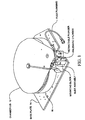
- One embodiment of the present invention is a process module assembly 10 for use in semiconductor manufacturing equipment. Suitable process modules include but are not limited to a bake module. As illustrated in Figure 1, assembly 10 includes a lid 12, a base plate 14 and a housing 16. Lid 12, base plate 14 and housing 16 define a process chamber.
- lid 12 is supported in a horizontal plane by a horizontal guide 18 and a vertical shaft 20 at a lid pivot point 22.
- Shaft 20 is supported in a bearing block 22 with two bushings 24. Together guide 22 and bushings 24 provide support for lid 12.
- Guide 22 is rigidly attached to a mounted block 26 located on base plate 14.
- Lid's 12 open and close motion can be accomplished with a pneumatic cylinder 28, or other suitable mechanical structure, attached between bearing block 22 and base plate 14.
- lid 12 In normal operation lid 12 is constrained from rotating with a suitable device including but not limited to a retractable spring plunger 30 located on bearing block 22.
- a suitable device including but not limited to a retractable spring plunger 30 located on bearing block 22.
- cylinder 28 In the up position, cylinder 28 is in its fully extended position. Lid 12 is supported in the horizontal plane by the reaction forces of horizontal guide 22 and bushings 24. Lid 12 can be cleaned or serviced in the "up" or open position.
- spring plunger 30 To rotate lid 12 spring plunger 30 is retracted. When spring plunger 30 is retracted lid 12 can be rotated to a position allowing access to clean an internal lid surfaces 32 which can include a shower head or other assembly that delivers a fluidic medium to the chamber..
- Bushings 24 allow lid 12 to be rotated about a vertical pivot axis. Substantially constant contact with horizontal guide 22 maintains lid 12 in a horizontal plane. Retracting spring plunger 30 and rotation of lid 12 is accomplished without removing or disassembling assembly 12.
- a flexible process gas tube 34 allows movement with lid 12 while remaining fixed (connected) at the opposite end.
- a chamber vacuum seal such as O-ring 36, provides a vacuum tight boundary and sealing surface of the process chamber.
- a controlled clearance between the lid support shaft and the bushings allows the sealing surface of the lid to lie parallel a top of housing 16. Additionally, the design allows for a small amount of vertical axis relative motion between the lid support shaft and bearing block due to variations in pneumatic cylinder stroke length and compression of the vacuum seal.
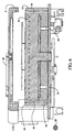
- process module assembly 10 is a bake module that includes an insulator 38, one or more reflective members 40, a hot plate 42 and housing 16.
- Reflective members 40 can have plate-type geometric configurations.
- Housing 16 has a diameter larger than the diameters of hot plate 42 and insulator 38, and a height that is approximately equal to the height of insulator 38 and hot plate 42.
- Lid 12 can include a shower heat 44.
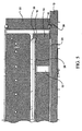
- Base plate 14 can include an exhaust port and an assembly to move lid 12, as described in Figures 2 and 3.
- Insulator 38 is positioned on base plate 14 in a manner to create a first air gap 46.
- First air gap 46 creates a conductive resistance layer between base plate 14 and the remaining elements of assembly 10.
- the diameter of first air gap 46 can be smaller than the diameter of insulator 38.
- Insulator 38 has a top surface with a recess 48. Recess 48 is dimensioned to receive one or more reflective members 40. As illustrated in Figure 4, three reflective members 40 are included. It will be appreciated that the present invention can include one reflective member 40, or any number of reflective members 40.
- An air gap 50 is formed between a top surface of insulator 38 and the lower most reflective member 40. Air gap 50 creates a conductive resistance layer. Air gaps are also formed between adjacent reflective members 40 to once again create conductive resistance layers.
- the top surfaces of reflective members 40 have high thermal reflectivity and low thermal absorptivity characteristics.
- the diameters of reflective members 40 are slightly smaller than the diameter of hot plate 42.
- An air gap 52 is formed between housing 16 and insulator 38 and hot plate 42. Hot gases surrounding hot plate 42 are removed by traveling from gap 52 and then through exhaust ports 54 that are formed in insulator 38.
- O-rings 60 and 36 are received in grooves 62 and 64.
- O-ring 60 provides a seal between housing 16 and base plate 14, while O-ring 36 creates a seal between housing 16 and lid 12.
- Process gases can be introduced to assembly 10 through a gas conduit 66.
- shower head 44 receives gases from gas conduit 66 and injects the gases onto a top surface of a wafer positioned adjacent to hot plate 42.
Applications Claiming Priority (7)
| Application Number | Priority Date | Filing Date | Title |
|---|---|---|---|
| US13956099P | 1999-06-16 | 1999-06-16 | |
| US139560P | 1999-06-16 | ||
| US20361200P | 2000-05-10 | 2000-05-10 | |
| US203612P | 2000-05-10 | ||
| US593270 | 2000-06-13 | ||
| US09/593,270 US6416318B1 (en) | 1999-06-16 | 2000-06-13 | Process chamber assembly with reflective hot plate and pivoting lid |
| EP00941486A EP1186007B1 (de) | 1999-06-16 | 2000-06-16 | Prozesskammer mit einer reflektierenden heizplatte |
Related Parent Applications (1)
| Application Number | Title | Priority Date | Filing Date |
|---|---|---|---|
| EP00941486A Division EP1186007B1 (de) | 1999-06-16 | 2000-06-16 | Prozesskammer mit einer reflektierenden heizplatte |
Publications (1)
| Publication Number | Publication Date |
|---|---|
| EP1536457A2 true EP1536457A2 (de) | 2005-06-01 |
Family
ID=34468403
Family Applications (1)
| Application Number | Title | Priority Date | Filing Date |
|---|---|---|---|
| EP05003989A Withdrawn EP1536457A2 (de) | 1999-06-16 | 2000-06-16 | Prozesskammer mit einer reflektierenden Platte |
Country Status (1)
| Country | Link |
|---|---|
| EP (1) | EP1536457A2 (de) |
-
2000
- 2000-06-16 EP EP05003989A patent/EP1536457A2/de not_active Withdrawn
Similar Documents
| Publication | Publication Date | Title |
|---|---|---|
| JP2005240173A (ja) | 基板支持用ブッシング | |
| US5753133A (en) | Method and apparatus for etching film layers on large substrates | |
| US6815349B1 (en) | Electroless copper deposition apparatus | |
| CN206657802U (zh) | 缓冲腔室和晶片传送机器人 | |
| US5879128A (en) | Lift pin and support pin apparatus for a processing chamber | |
| US5895549A (en) | Method and apparatus for etching film layers on large substrates | |
| JP3263684B2 (ja) | 基板搬送用ロボット | |
| CN100461363C (zh) | 搬运机械手以及搬运装置 | |
| US6416318B1 (en) | Process chamber assembly with reflective hot plate and pivoting lid | |
| JP6639657B2 (ja) | 熱質量が小さい加圧チャンバ | |
| JP4547119B2 (ja) | 真空処理装置 | |
| JP2003526895A (ja) | 真空処理装置においてウェーハを前処理及び後処理するための枚葉式ウェーハロードロックチャンバ | |
| US6303906B1 (en) | Resistively heated single wafer furnace | |
| JP2003249541A (ja) | ウエハステージ | |
| JP2024539714A (ja) | 化学気相堆積装置およびその方法 | |
| US20010040230A1 (en) | Compact gate valve | |
| US20040045813A1 (en) | Wafer processing apparatus, wafer stage, and wafer processing method | |
| US6091056A (en) | Hot plate oven for processing flat panel displays and large wafers | |
| JP3908678B2 (ja) | ウエハ処理方法 | |
| JP7821881B2 (ja) | エピタキシャル反応デバイス | |
| JP2004087869A (ja) | ウエハ処理装置、ウエハステージおよびウエハ処理方法 | |
| US6709470B2 (en) | Benchtop processing | |
| JPH04330722A (ja) | ウェーハ処理装置 | |
| US20260003288A1 (en) | Bowl and substrate treatment apparatus | |
| US20250372408A1 (en) | Valve apparatuses and related methods for reactive process gas isolation and facilitating purge during isolation |
Legal Events
| Date | Code | Title | Description |
|---|---|---|---|
| PUAI | Public reference made under article 153(3) epc to a published international application that has entered the european phase |
Free format text: ORIGINAL CODE: 0009012 |
|
| 17P | Request for examination filed |
Effective date: 20050309 |
|
| AC | Divisional application: reference to earlier application |
Ref document number: 1186007 Country of ref document: EP Kind code of ref document: P |
|
| AK | Designated contracting states |
Kind code of ref document: A2 Designated state(s): AT BE CH CY DE DK ES FI FR GB GR IE IT LI LU MC NL PT SE |
|
| RAP1 | Party data changed (applicant data changed or rights of an application transferred) |
Owner name: ASML HOLDING N.V. |
|
| STAA | Information on the status of an ep patent application or granted ep patent |
Free format text: STATUS: THE APPLICATION IS DEEMED TO BE WITHDRAWN |
|
| 18D | Application deemed to be withdrawn |
Effective date: 20100105 |