EP1536438A2 - Multilayer ceramic capacitor - Google Patents
Multilayer ceramic capacitor Download PDFInfo
- Publication number
- EP1536438A2 EP1536438A2 EP04028193A EP04028193A EP1536438A2 EP 1536438 A2 EP1536438 A2 EP 1536438A2 EP 04028193 A EP04028193 A EP 04028193A EP 04028193 A EP04028193 A EP 04028193A EP 1536438 A2 EP1536438 A2 EP 1536438A2
- Authority
- EP
- European Patent Office
- Prior art keywords
- dielectric
- internal electrode
- electrode layer
- dielectric layer
- temperature
- Prior art date
- Legal status (The legal status is an assumption and is not a legal conclusion. Google has not performed a legal analysis and makes no representation as to the accuracy of the status listed.)
- Granted
Links
Images


Classifications
-
- H—ELECTRICITY
- H01—ELECTRIC ELEMENTS
- H01G—CAPACITORS; CAPACITORS, RECTIFIERS, DETECTORS, SWITCHING DEVICES, LIGHT-SENSITIVE OR TEMPERATURE-SENSITIVE DEVICES OF THE ELECTROLYTIC TYPE
- H01G4/00—Fixed capacitors; Processes of their manufacture
- H01G4/002—Details
- H01G4/018—Dielectrics
- H01G4/06—Solid dielectrics
- H01G4/08—Inorganic dielectrics
- H01G4/12—Ceramic dielectrics
-
- H—ELECTRICITY
- H01—ELECTRIC ELEMENTS
- H01G—CAPACITORS; CAPACITORS, RECTIFIERS, DETECTORS, SWITCHING DEVICES, LIGHT-SENSITIVE OR TEMPERATURE-SENSITIVE DEVICES OF THE ELECTROLYTIC TYPE
- H01G4/00—Fixed capacitors; Processes of their manufacture
- H01G4/30—Stacked capacitors
Definitions
- the present invention relates to a multilayer ceramic capacitor.
- JP-A-2003-124049 there has been proposed a technique for realizing high dielectric permittivity without deteriorating electric characteristics by controlling the structure of an interlayer dielectric layer in a multilayer ceramic capacitor composed of a dielectric layer and an internal electrode layer.
- the interlayer dielectric layer includes a plurality of dielectric particles, and the plurality of dielectric particles are composed of contact dielectric particles contacting the internal electrode layer and noncontact dielectric particles not contacting the internal electrode layer.
- JP-A-2003-124049 describes to use an internal electrode layer paste added with an additive component for accelerating grain growth, but a composition of the additive component is different from that of dielectric particles.
- An object of the present invention is to provide a multilayer ceramic capacitor, wherein an improvement of a bias characteristic at 85°C can be expected even when the interlayer dielectric layer is made thin.
- a multilayer ceramic capacitor having an internal electrode layer and an interlayer dielectric layer having a thickness of 3.5 ⁇ m or less, wherein:
- a multilayer ceramic capacitor according to the present invention can be produced, for example, by a method explained below. Note that a production method of the multilayer ceramic capacitor of the present invention is not limited to the method below.
- the method includes a step of firing a multilayer body obtained by using a dielectric layer paste including a dielectric material and an internal electrode layer paste including a main component of an adding dielectric material having the same composition as that of the dielectric material, an average particle diameter of 0.01 to 0.2 ⁇ m, and a pH of 7.5 or more.
- the firing step is a step for raising an atmosphere temperature toward a firing holding temperature T2, holding the T2 for a predetermined time, then, lowering.
- the respective steps of temperature raising, holding T2 and temperature lowering are not particularly limited in detail.
- a multilayer ceramic capacitor wherein an improvement of a bias characteristic at 85°C (a change amount of a capacity when applying a predetermined bias voltage at 85°C comparing with the capacity at the room temperature) can be expected even when the interlayer dielectric layer is made thin, is provided.
- a multilayer ceramic capacitor comprising an internal electrode layer and a dielectric layer
- an explanation will be made on a multilayer ceramic capacitor, wherein a plurality of internal electrode layers and dielectric layers are alternately stacked, as an example.
- a multilayer ceramic capacitor 1 according to an embodiment of the present invention comprises a capacitor element body having the configuration of alternately stacking interlayer dielectric layers 2 and internal electrode layers 3.
- a pair of external electrodes 4 are formed to connect respectively to the internal electrode layers 3 alternately arranged inside the element body 10.
- the internal electrodes layers 3 are stacked, so that the respective end faces are alternately exposed to surfaces of two facing end portions of the capacitor element body 10.
- the pair of external electrodes 4 are formed on both end portions of the capacitor element body 10 and connected to exposed end faces of the alternately arranged internal electrode layers 3 to compose a capacitor circuit.
- a shape of the capacitor element body 10 is not particularly limited and normally is a rectangular parallelepiped shape. Also, dimensions thereof are not particularly limited and may be suitable dimensions in accordance with the use object, but normally are a length of (0.6 to 5.6 mm) ⁇ a width of (0.3 to 5.0 mm) ⁇ a height of (0.3 to 1.9 mm) or so.
- external dielectric layers 20 are arranged on both external end portions in the stacking direction of the internal electrode layers 3 and interlayer dielectric layers 2 to protect inside the element body 10.
- a composition of the interlayer dielectric layer 2 and the external dielectric layer 20 is not particularly limited in the present invention, but is composed, for example, of a dielectric ceramic composition below.
- a dielectric ceramic composition of the present embodiment is, for example, a dielectric ceramic composition including barium titanate as a main component.
- subcomponents to be included with the main component in the dielectric ceramic composition those containing at least one kind of Mn, Cr, Si, Ca, Ba, Mg, V, W, Ta, Nb, R (R is Y, at least one kind of rare earth elements), an oxide of Si, and compounds to be oxides by firing, may be mentioned. By adding a subcomponent, characteristics as a capacitor can be obtained even by firing in a reduced atmosphere.
- a minute amount of components such as C, F, Li, Na, K, P, S and Cl, may be contained by about 0.1 wt% or less.
- a composition of the interlayer dielectric layer 2 and the external dielectric layer 20 is not limited to the above in the present invention. In the present embodiment, it is preferable to use those having a composition below as the interlayer dielectric layer 2 and the external dielectric layer 20.
- the composition is to contain barium titanate as a main component, a magnesium oxide and an oxide of a rare earth element as subcomponents, at least one kind selected from a barium oxide and a calcium oxide, and at least one kind selected from a silicon oxide, a manganese oxide, a vanadium oxide and a molybdenum oxide as still other subcomponents.
- a barium titanate in terms of BaTiO 3 when expressing a barium titanate in terms of BaTiO 3 , a magnesium oxide in terms of MgO, an oxide of a rare earth element in terms of R 2 O 3 , a barium oxide in terms of BaO, a calcium oxide in terms of CaO, a silicon oxide in terms of SiO 2 , manganese oxide in terms of MnO, vanadium oxide in terms of V 2 O 5 and molybdenum oxide in terms of MoO 3 , respectively; ratios with respect to 100 moles of BaTiO 3 are MgO by 0.1 to 3 moles, R 2 O 3 by more than 0 mol but not more than 5 moles, BaO + CaO by 2 to 12 moles, SiO 2 by 2 to 12 moles, MnO by more than 0 mole but not more than 0.5 mole, V 2 O 5 by 0 to 0.3 mole and MoO 3 by 0 to 0.3 mole.
- a thickness of the interlayer dielectric layer 2 is made to be as thin as preferably 3.5 ⁇ m or less and more preferably 2.5 ⁇ m or less.
- a bias characteristic at 85°C of the capacitor 1 is improved even when the thickness of the interlayer dielectric layer 2 is made thin as such.
- the number of stacked layers of the interlayer dielectric layer 2 may be suitably determined in accordance with the object and use, but normally is as large as 50 layers or more in many cases.
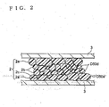
- the interlayer dielectric layer 2 comprises at least dielectric particles (contact dielectric particles) 2b contacting the internal electrode layer 3, dielectric particles (noncontact dielectric particles) 2b not contacting the internal electrode layer and a grain boundary phase 2c.
- the contact dielectric particles 2a contact one of a pair of internal electrode layers 3 sandwiching the interlayer dielectric layer 2 including the contact dielectric particles 2a, and do not contact the both.
- an average particle diameter of the contact dielectric particles 2a is indicated by D50e
- an average particle diameter of the noncontact dielectric particles 2b is indicated by D50d.
- the ratio of D50e and D50d (D50e/D50d) satisfies 1.20 to 3.00 (note that 1.20 and 3.00 are excluded). Preferably it satisfies 1.30 to 2.50 and more preferably 1.30 to 2.32.
- the (D50e/D50d) value is too small, a sufficient effect of improving the bias characteristic at 85°C cannot be obtained when the interlayer dielectric layer 2 is made thin, while when too large, there arise disadvantages, such that the defective rate of initial insulation resistance (IR) increases, etc.
- the D50e is less than 0.450 ⁇ m, preferably 0.300 ⁇ m or less. Even when the ratio of D50e and D50d (D50e/D50d) is in a suitable range, when the D50 is too great, the effect of improving the bias characteristic at 85°C is deteriorated. On the other hand, when the D50e is too small, it becomes difficult to set the (D50e/D50d) value in a suitable range, therefore, the lower limit of the D50e is preferably 0.150 ⁇ m.
- the D50d is preferably 0.050 to 0.300 ⁇ m, more preferably 0.100 to 0.200 ⁇ m.
- the D50d is too great, it may cause disadvantages, such that the insulation resistance defective rate becomes high, etc. when making the dielectric layer thin.
- the D50d is too small, a sufficient electrostatic capacity as a capacitor cannot be obtained.
- the D50e and D50d are defined as below.
- the "D50e” is a value obtained by cutting in the dielectric stacking direction, measuring an average area of a section shown in FIG. 2 of 300 or more of dielectric particles 2a contacting an internal electrode, calculating the diameter by a diameter of the equivalent circle and multiplying the result with 1.5.
- the "D50d” is a value obtained by measuring an average area of a section shown in FIG. 2 of 300 or more of dielectric particles 2b not contacting an internal electrode, calculating the diameter by a diameter of the equivalent circle and multiplying the result with 1.5.
- D50e and D50d mean average particle diameters of the contact dielectric particles 2a and noncontact dielectric particles 2b in the interlayer dielectric layer 2 (a portion contributing to an electrostatic capacity) sandwiched between the internal electrode layers 3.
- the grain boundary phase 2c normally comprises an oxide of a material composing the dielectric material or internal electrode material, an oxide of a separately added material and, furthermore, an oxide of a material to be mixed as an impurity in a step.
- the internal electrode layer 3 shown in FIG. 1 is composed of a base metal conductive material substantially serving as an electrode.
- a base metal to be used as a conductive material Ni or a Ni alloys is preferable.
- a Ni alloy an alloy of Ni and at least one kind selected from Mn, Cr, Co, Al, Ru, Rh, Ta, Re, Os, Ir, Pt and W, etc. is preferable, and a content of Ni in the alloy is preferably 95 wt% or more.
- Ni or the Ni alloy may contain a variety of minute amount of components, such as P, C, Nb, Fe, Cl, B, Li, Na, K, F and S, by about 0.1 wt% or less.
- a thickness of the internal electrode layer 3 is made thin to preferably 2.0 ⁇ m or less, more preferably 1.2 ⁇ m or less.
- the external electrode 4 shown in FIG. 1 at least one kind of Ni, Pd, Ag, Au, Cu, Pt, Rh, Ru and Ir, etc. or an alloy of these may be normally used. Normally, Cu, a Cu alloy, Ni or a Ni alloy, etc., Ag, a Ag-Pd alloy, an In-Ga alloy, etc. are used. A thickness of the external electrode 4 may be suitably determined in accordance with use, but normally 10 to 200 ⁇ m or so is preferable.
- a dielectric layer paste to compose the interlayer dielectric layer 2 and the external dielectric layer 20 shown in FIG. 1 after firing and an internal electrode layer paste to compose the internal electrode layer 3 shown in FIG. 1 after firing are prepared.
- the dielectric layer paste is produced by kneading a dielectric material and organic vehicle.
- a dielectric material may be suitably selected from a variety of compounds to be composite oxides and oxides, such as carbonate, nitrate salt, hydroxides and organic metal compounds, and mixed for use.
- the dielectric material is normally used as powder having an average particle diameter of 0.4 ⁇ m or less, preferably 0.1 to 3.0 ⁇ m or so.
- An organic vehicle contains a binder and a solvent.
- a binder a variety of normal binders, for example, ethyl cellulose, polyvinyl butyral and an acrylic resin, etc. may be used.
- the solvent is not particularly limited, and terpineol, acetone, toluene, xylene, ethanol and other organic solvents are used.
- the dielectric layer paste may be formed by kneading the dielectric material and vehicle obtained by dissolving a water-soluble binder in water.
- the water-soluble binder is not particularly limited, and polyvinyl alcohol, methyl cellulose, hydroxyl ethyl cellulose, water-soluble acrylic resin and emulsion, etc. may be used.
- a content of respective components in the dielectric layer paste is not particularly limited and the dielectric paste may be produced to contain, for example, about 1 to 50 wt% of the solvent.
- the dielectric layer paste may contain additives selected from a variety of dispersants, plasticizers, dielectrics, subcomponent compounds, glass frits, insulators, etc. in accordance with needs.
- the total content is preferably made to be about 10 wt% or less.
- the internal electrode layer paste is produced by kneading a conductive material, a main component of an adding dielectric material and an organic vehicle.
- the conductive material Ni, a Ni alloy, furthermore, a mixture of these are used.
- a shape of such conductive materials is not particularly limited, and may be a spherical shape, a scale like shape, or a combined shape of these.
- conductive materials having an average particle diameter of 0.5 ⁇ m or less, preferably 0.01 to 0.4 ⁇ m or so are supposed to be normally used in the case of a spherical shape. It is to realize a thin layer on a higher level.
- the conductive material is contained in the internal electrode layer paste preferably by 35 to 60 wt%.
- a main component of the adding dielectric material exhibits an effect of suppressing sintering of internal electrodes (conductive material) in the firing process.
- a main component of the adding dielectric material preferably has the same composition as that of the dielectric material included in the above dielectric layer paste. As a result of having the same composition, change of a composition of the dielectric layer due to dispersion from the internal electrode layer to the dielectric layer is not caused.
- the main component of the adding dielectric material preferably has a pH of a specific range. It was found by the present inventors that by using a dielectric material having a specific pH for adding, the ratio of D50e/D50d became large and a bias characteristic at 85°C of a finally obtained capacitor 1 could be improved.
- a pH of the main component of the adding dielectric material (particularly, a main component material contained in the dielectric material) is preferably 7.5 or more, more preferably 8 to 11.
- an average particle diameter of the main component of the adding dielectric material may be the same as particle diameters of the dielectric material included in the dielectric layer paste, but the smaller the more preferable, and is preferably 0.01 to 0.2 ⁇ m, particularly preferably 0.01 to 0.15 ⁇ m.
- the main component of the adding dielectric material included in the internal electrode layer paste is preferably 5 to 30 wt%, more preferably 10 to 20 wt% with respect to the conductive material.
- the organic vehicle contains a binder and a solvent.
- binder for example, ethyl cellulose, an acrylic resin, polyvinyl butyral, polyvinyl acetal, polyvinyl alcohol, polyolefin, polyurethane, polystyrene or copolymers of these may be mentioned.
- the binder is contained in the internal electrode layer paste preferably by 1 to 5 wt% with respect to mixed powder of the conductive material and the main component of the adding dielectric material.
- any of well known solvents such as terpineol, dihydroterpineol, butycarbitol, kerosene, etc. may be used.
- a content of the solvent is preferably 20 to 50 wt% or so with respect to the whole paste.
- the internal electrode layer paste may contain a plasticizer.
- a plasticizer benzyl butyl phthalate (BBP) and other phthalate esters, adipic acid, phosphoric ester and glycols, etc. may be mentioned.
- a green chip is produced.
- the dielectric layer paste and the internal electrode layer paste in a predetermined pattern are printed by stacking on a carrier sheet, cut to be a predetermined shape, and peeled from the carrier sheet to obtain a green chip.
- a green sheet obtained by forming the dielectric layer paste on the carrier sheet to be a predetermined thickness is formed, the internal electrode layer paste is printed thereon to be a predetermined pattern, then, the results are stacked to obtain a green chip.
- the binder removing is a step for raising an atmosphere temperature T0, for example, from the room temperature, (25°C) toward a binder removing holding temperature T1 at a predetermined temperature raising rate, holding at the T1 for a predetermined time, then, lowering at a predetermined temperature lowering rate, for example, as shown in FIG. 3.
- the temperature raising rate is preferably 5 to 300°C/hour, more preferably 10 to 100°C/hour.
- the binder removing holding temperature T1 is preferably 200 to 400°C, and more preferably 220 to 380°C.
- the holding time at the T1 is preferably 0.5 to 24 hours, and more preferably 2 to 20 hours.
- the temperature lowering rate is preferably 5 to 300°C/hour, more preferably 10 to 100°C/hour.
- the atmosphere for the binder removing processing is preferably in the air or in a reducing atmosphere.
- an atmosphere gas in a reducing atmosphere is preferably, for example, a wet mixed gas of N 2 and H 2 .
- An oxygen partial pressure in the processing atmosphere is preferably 10 -45 to 10 5 Pa. When the oxygen partial pressure is too low, the binder removing effect declines, while when too high, the internal electrode layer is liable to be oxidized.
- the firing is a step for raising the atmosphere temperature T0, for example, from the room temperature (25°C) toward a firing holding temperature T2 at a predetermined temperature raising rate, holding at the T2 for a predetermined time, and lowering the atmosphere temperature at a predetermined temperature lowering rate, for example, as shown in FIG. 3 (refer to a solid line portion in FIG. 3).
- the temperature raising rate is preferably 50 to 500°C/hour, more preferably 100 to 300°C/hour.
- the firing holding temperature T2 is preferably 1100 to 1300°C, more preferably 1150 to 1250°C.
- the holding time at the T2 is preferably 0.5 to 8 hours, more preferably 1 to 3 hours.
- the temperature lowering rate is preferably 50 to 500°C/hour, more preferably 150 to 300°C/hour.
- the processing atmosphere of firing is preferably a reducing atmosphere.
- a reducing atmosphere for example, a wet mixed gas of N 2 and H 2 is preferable.
- An oxygen partial pressure in the firing atmosphere is preferably 6 ⁇ 10 -9 to 10 -4 Pa.
- the oxygen partial pressure is too low, the conductive material of the internal electrode layer causes abnormal sintering and results in breaking, while when too high, the internal electrode layer is liable to be oxidized.
- the atmosphere temperature T0 may be held at a predetermined temperature T4 before reaching the T2 for a predetermined time, then, raised to the firing holding temperature T2.
- T4 By keeping for a predetermined time at the T4 before reaching the T2, it is possible to obtain an effect of making the D50e/D50d value larger (improvement of the bias characteristic at 85°C) and an effect of obtaining a desired structure even when using a main component of an adding dielectric material having a lower pH than 6.
- the bias characteristic at 85°C is furthermore improved.
- the bias characteristics at 85°C can be improved in an obtained multilayer ceramic capacitor 1.
- the T4 in this case is preferably 400 to 1050°C, more preferably 600 to 1000°C.
- the holding time at the T4 is preferably 0.5 to 10 hours, more preferably 1 to 2 hours.
- Annealing is processing to re-oxidize the dielectric layer and, thereby, characteristics of a finally obtained capacitor are obtained.
- Annealing is a step for raising an atmosphere temperature T0, for example, from the room temperature (25°C) toward an annealing holding temperature T3 at a predetermined temperature raising rate, holding the T3 for a predetermined time and lowering the atmosphere temperature T0 at a predetermined temperature lowering rate.
- the temperature raising rate is preferably 100 to 300°C/hour, more preferably 150 to 250°C/hour.
- the annealing holding temperature T3 is preferably 800 to 1100°C, more preferably 900 to 1100°C.
- the holding time at the T3 is preferably 0 to 20 hours, more preferably 2 to 10 hours.
- the T3 is too low, oxidization of the dielectric layer 2 becomes insufficient, so that it is liable that the IR becomes low and the IR lifetime becomes short.
- the T3 is too high, not only the internal electrode layer 3 is oxidized to reduce the capacity, but also the internal electrode layer 3 reacts with a dielectric base material, and it is liable to easily cause deterioration of the capacity-temperature characteristic, deterioration of the IR and deterioration of the IR lifetime.
- the temperature lowering rate is preferably 50 to 500°C/hour, more preferably 100 to 300°C/hour.
- a processing atmosphere of annealing is preferably a neutral atmosphere.
- an atmosphere gas in a neutral atmosphere for example, a wet N 2 gas is preferably used.
- the atmosphere may be changed after raising the temperature to the holding temperature T3 in a N 2 gas atmosphere, or the entire annealing process may be performed in a wet N 2 gas atmosphere.
- An oxygen partial pressure in the annealing atmosphere is preferably 2 ⁇ 10 -4 to 1 Pa. When the oxygen partial pressure is too low, re-oxidization of the dielectric layer 2 is difficult, while when too high, the internal electrode layer 3 is liable to be oxidized.
- the annealing may be composed only of a temperature raising step and a temperature lowering step.
- the temperature holding time may be zero.
- the holding temperature T3 is the same as the highest temperature.
- a wetter for example, a wetter, etc. may be used to wet a N 2 gas and a mixed gas, etc.
- the water temperature is preferably 0 to 75°C or so.
- a capacitor element body 10 composed of a sintered body is formed.
- an external electrode 4 is formed on the obtained capacitor element body.
- the external electrode 4 can be formed by a well known method of polishing end faces of the capacitor element body 10 composed of the above sintered body, for example, by barrel polishing and sandblasting, then, burning on the both end faces an external electrode paste normally including at least one kind of Ni, Pd, Ag, Au, Cu, Pt, Rh and Ir, etc. or an alloy of these, or applying an In-Ga alloy, etc.
- a covering layer may be formed by soldering, etc. on a surface of the external electrode 4.
- the binder removing processing, firing and annealing are performed independently, but the present invention is not limited to this and at least two steps may be successively performed.
- the atmosphere is changed without cooling, continuously, the temperature is raised to the firing holding temperature T2 to perform firing, then cooled, and the atmosphere is changed when reaching to the annealing holding temperature T3 to perform annealing.
- a dielectric material a dielectric material, a PVB (polyvinyl butyral) resin as a binder, DOP (dioctylphthalate) as a plasticizer, and ethanol as a solvent were prepared.
- the dielectric material was produced by performing wet mixing by a ball-mill for 16 hours on 0.2 mole% of MnCO 3 , 0.5 mole% of MgO, 0.3 mole% of V 2 O 5 , 2 mole% of Y 2 O 3 , 3 mole% of CaCO 3 , 3 mole% of BaCO 3 and 3 mole% of SiO 2 as subcomponent materials with respect to BaTiO 3 having an average particle diameter of 0.2 ⁇ m or so as a main component material, and drying the result.
- Ni particles having an average particle diameter of 0.2 ⁇ m as a conductive material, a main component of an adding dielectric material having the same composition as that of the dielectric material contained in the dielectric layer paste and having an average particle diameter and a pH shown in Table 1, an ethyl cellulose resin as a binder, and terpineol as a solvent were prepared.
- the average particle diameter and pH of the main component of the adding dielectric material in Table 1 are values (an average particle diameter of 0.025 to 0.3 ⁇ m and a pH of 7.5 to 11) of BaTiO 3 as a main component material used in producing the dielectric material.
- the pH value in Table 1 is a value obtained by adding 30g of BaTiO 3 as material powder to 100 ml of ion-exchange water, agitating the result by ultrasonic dispersion for 5 minutes, leaving it still for 100 hours, then, measuring the supernatant portion by a pH meter.
- a multilayer ceramic chip capacitor 1 shown in FIG. 1 was produced as explained below.
- the ceramic green sheet is referred to as a first green sheet and prepared by two or more.
- the internal electrode layer paste was formed to be a predetermined pattern by a screen printing method to obtain a ceramic green sheet having an electrode pattern of a thickness of 1.5 ⁇ m.
- this ceramic green sheet is referred to as a second green sheet and prepared by two or more.
- the first green sheets were stacked to be a thickness of 300 ⁇ m to form a green sheet group.
- a green sheet group five of the second green sheets were stacked, furthermore, a same green sheet group as above was formed by being stacked thereon, and the result was heated and pressurized under a condition of a temperature of 80°C and a pressure of 1 ton/cm 2 to obtain a green multilayer body.
- the obtained multilayer body is cut to be a size of a length of 3.2 mm ⁇ a width of 1.6 mm ⁇ a height of 1.0 mm, and subjected to binder removing processing, firing and annealing under the conditions below to obtain a sintered body.
- FIG. 3 shows a graph of respective temperature changes in the binder removing processing, firing and annealing.
- the binder removing was performed under a condition that a temperature raising rate was 30°C/hour, a holding temperature T1 was 250°C, a holding time was 8 hours, a temperature lowering rate was 200°C/hour, and a processing atmosphere was in the air.
- Firing was performed under a condition that a temperature raising rate was 200°C/hour, a holding temperature T2 was 1240°C, a holding time was 2 hours, a temperature lowering rate was 200°C/hour, and a processing atmosphere was in a reducing atmosphere (a mixed gas of N 2 and H 2 was adjusted by passing through steam under an oxygen partial pressure of 10 -6 Pa).
- the annealing was performed under a condition that a temperature raising rate was 200°C/hour, a holding temperature T3 was 1050°C, a holding time was 2 hours, a temperature lowering rate was 200°C/hour, and a processing atmosphere was in a neutral atmosphere (a N 2 gas was adjusted by passing through steam under an oxygen partial pressure of 0.1 Pa).
- a particle diameter D was obtained by cutting the obtained sintered body on a face perpendicular to the stacking direction of the internal electrode layers, polishing the face, performing thermal etching processing (at 1200°C for 10 minutes), observing the particles by a scanning electronic microscope (SEM), converting a particle area to a circle area, and multiplying the diameter by 1.5.
- SEM scanning electronic microscope
- end faces of the obtained sintered body were polished by sandblasting, then, an In-Ga alloy was applied to form a test electrode, so that multilayer ceramic chip capacitor samples were obtained.
- Dimensions of the capacitor samples were a length of 3.2 mm ⁇ a width of 1.6 mm ⁇ a height of 1.0 mm.
- a thickness of the dielectric layer 2 was 1.0 ⁇ m, and a thickness of the internal electrode layer 3 was 1.2 ⁇ m.
- a bias characteristic at 85°C was evaluated on the obtained capacitor samples.
- the bias characteristic of capacitors at 85°C was evaluated by measuring the obtained capacitor samples by an LCR meter under 1 kHz, 0.7 Vrms and a bias voltage of 2.6 V in a constant chamber held at 85°C, and calculating a capacity change rate from a value measured without applying a bias voltage at 20°C.
- the evaluation standard was set that those becoming higher than -21.0% were preferable. The results are shown in Table 1.
- the bias characteristic at 85°C is deteriorated in the samples 7 to 9 and 11 to 12, wherein (D50e/D50d) is out of a range of more than 1.20 but less than 3.00. Even when the (D50e/D50d) is in the range of the present invention, the bias characteristic at 85°C is deteriorated also in the sample 10, wherein the D50e is out of a range of less than 0.450 ⁇ m. Note that in a sample 13, the (D50e/D50d) value was too large as 3.00, so that the defective rate of the initial insulation resistance (IR) was increased and the IR defective was extremely much, therefore, the bias characteristic at 85°C was not evaluated.
- the electrostatic capacity change rate from 25°C to 85°C, wherein the reference was 20°C was within ⁇ 10%, and the bias characteristic at 85°C was excellent.
- the (D50e/D50d) value was larger and an effect of improving the bias characteristic was larger comparing with that in the sample 3.
Landscapes
- Engineering & Computer Science (AREA)
- Power Engineering (AREA)
- Chemical & Material Sciences (AREA)
- Manufacturing & Machinery (AREA)
- Microelectronics & Electronic Packaging (AREA)
- Ceramic Engineering (AREA)
- Inorganic Chemistry (AREA)
- Ceramic Capacitors (AREA)
- Fixed Capacitors And Capacitor Manufacturing Machines (AREA)
Abstract
Description
a multilayer ceramic capacitor, having an internal electrode layer and an interlayer dielectric layer having a thickness of 3.5 µm or less, wherein:
A dielectric ceramic composition of the present embodiment is, for example, a dielectric ceramic composition including barium titanate as a main component.
As subcomponents to be included with the main component in the dielectric ceramic composition, those containing at least one kind of Mn, Cr, Si, Ca, Ba, Mg, V, W, Ta, Nb, R (R is Y, at least one kind of rare earth elements), an oxide of Si, and compounds to be oxides by firing, may be mentioned. By adding a subcomponent, characteristics as a capacitor can be obtained even by firing in a reduced atmosphere. Nota that as an impurity, a minute amount of components, such as C, F, Li, Na, K, P, S and Cl, may be contained by about 0.1 wt% or less. Note that a composition of the interlayer
In the present embodiment, it is preferable to use those having a composition below as the interlayer
The composition is to contain barium titanate as a main component, a magnesium oxide and an oxide of a rare earth element as subcomponents, at least one kind selected from a barium oxide and a calcium oxide, and at least one kind selected from a silicon oxide, a manganese oxide, a vanadium oxide and a molybdenum oxide as still other subcomponents. Also, when expressing a barium titanate in terms of BaTiO3, a magnesium oxide in terms of MgO, an oxide of a rare earth element in terms of R2O3, a barium oxide in terms of BaO, a calcium oxide in terms of CaO, a silicon oxide in terms of SiO2, manganese oxide in terms of MnO, vanadium oxide in terms of V2O5 and molybdenum oxide in terms of MoO3, respectively; ratios with respect to 100 moles of BaTiO3 are MgO by 0.1 to 3 moles, R2O3 by more than 0 mol but not more than 5 moles, BaO + CaO by 2 to 12 moles, SiO2 by 2 to 12 moles, MnO by more than 0 mole but not more than 0.5 mole, V2O5 by 0 to 0.3 mole and MoO3 by 0 to 0.3 mole.
Note that the number of stacked layers of the interlayer
The T4 in this case is preferably 400 to 1050°C, more preferably 600 to 1000°C. The holding time at the T4 is preferably 0.5 to 10 hours, more preferably 1 to 2 hours.
The temperature lowering rate is preferably 50 to 500°C/hour, more preferably 100 to 300°C/hour.
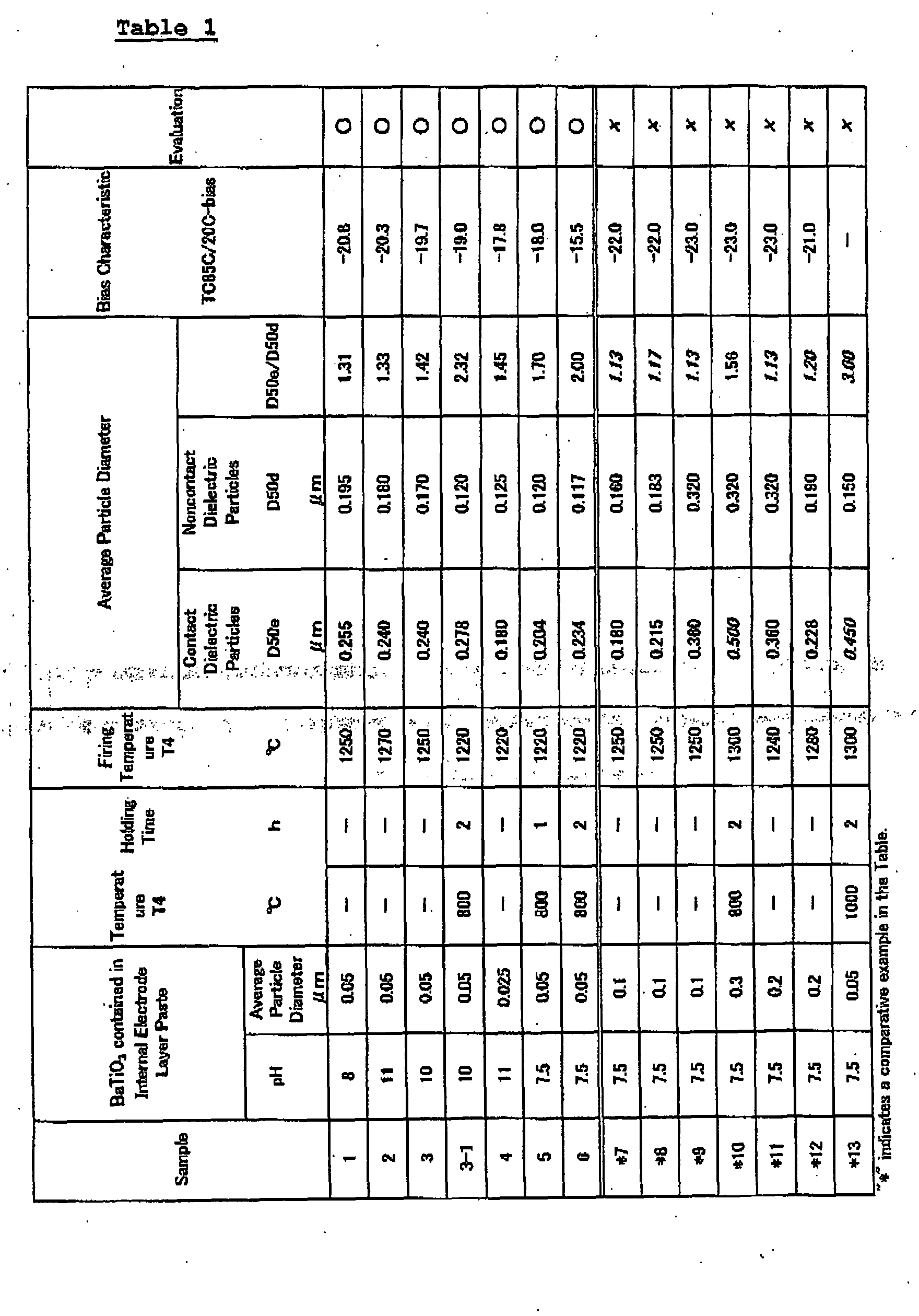
On the other hand, it was confirmed that, in the samples 1 to 6 in the range of the present invention, the electrostatic capacity change rate from 25°C to 85°C, wherein the reference was 20°C, was within ±10%, and the bias characteristic at 85°C was excellent. Particularly, in the sample 3-1, it is known that the (D50e/D50d) value was larger and an effect of improving the bias characteristic was larger comparing with that in the
Claims (3)
- A multilayer ceramic capacitor, having an internal electrode layer and a dielectric layer having a thickness of 3.5 µm or less, wherein:said dielectric layer is composed of contact dielectric particles contacting said internal electrode layer and noncontact dielectric particles not contacting said internal electrode layer; andwhen assuming that an average particle diameter of the contact dielectric particles is D50e and an average particle diameter of the noncontact dielectric particles is D50d, D50e < 0.450 µm and (D50e/D50d) = 1.20 to 3.00 (note that 1.20 and 3.00 are excluded) are satisfied.
- Method of producing a multilayer ceramic capacitor, comprising the step of firing a multilayer body obtained by using a dielectric layer paste including a dielectric material and an internal electrode layer paste including a main component of an adding dielectric material having the same composition as that of the dielectric material, an average particle diameter of 0.01 to 0.2 µm, and a pH of 7.5 or more.
- The method of claim 2, wherein the firing step comprises raising an atmosphere temperature toward a firing holding temperature T2, holding the T2 for a predetermined time, then, lowering.
Applications Claiming Priority (2)
| Application Number | Priority Date | Filing Date | Title |
|---|---|---|---|
| JP2003399006 | 2003-11-28 | ||
| JP2003399006A JP2005159224A (en) | 2003-11-28 | 2003-11-28 | Laminated ceramic capacitor |
Publications (3)
| Publication Number | Publication Date |
|---|---|
| EP1536438A2 true EP1536438A2 (en) | 2005-06-01 |
| EP1536438A3 EP1536438A3 (en) | 2008-08-06 |
| EP1536438B1 EP1536438B1 (en) | 2013-06-05 |
Family
ID=34463874
Family Applications (1)
| Application Number | Title | Priority Date | Filing Date |
|---|---|---|---|
| EP04028193.3A Expired - Lifetime EP1536438B1 (en) | 2003-11-28 | 2004-11-26 | Multilayer ceramic capacitor |
Country Status (6)
| Country | Link |
|---|---|
| US (1) | US7072170B2 (en) |
| EP (1) | EP1536438B1 (en) |
| JP (1) | JP2005159224A (en) |
| KR (1) | KR100651021B1 (en) |
| CN (1) | CN100521003C (en) |
| TW (1) | TWI249754B (en) |
Families Citing this family (25)
| Publication number | Priority date | Publication date | Assignee | Title |
|---|---|---|---|---|
| US7507682B2 (en) * | 2004-02-24 | 2009-03-24 | Kyocera Corporation | Method of manufacturing ceramic paste and ceramic multi-layer wiring substrate utilizing the same |
| JP4073416B2 (en) * | 2004-03-31 | 2008-04-09 | Tdk株式会社 | Multilayer ceramic capacitor |
| US7224570B2 (en) * | 2004-06-28 | 2007-05-29 | Kyocera Corporation | Process for preparing multilayer ceramic capacitor and the multilayer ceramic capacitor |
| US20060012282A1 (en) * | 2004-07-15 | 2006-01-19 | Ngk Insulators, Ltd. | Dielectric device |
| TW200705481A (en) * | 2005-04-28 | 2007-02-01 | Tdk Corp | Method of production of multilayer ceramic electronic device |
| JP4635928B2 (en) * | 2006-03-27 | 2011-02-23 | Tdk株式会社 | Multilayer electronic component and manufacturing method thereof |
| US7859823B2 (en) * | 2007-06-08 | 2010-12-28 | Murata Manufacturing Co., Ltd. | Multi-layered ceramic electronic component |
| JP4510116B2 (en) * | 2008-06-20 | 2010-07-21 | 富士通株式会社 | Capacitor manufacturing method, structure, and capacitor |
| JP5276137B2 (en) | 2011-04-13 | 2013-08-28 | 太陽誘電株式会社 | Multilayer capacitor |
| KR101872520B1 (en) * | 2011-07-28 | 2018-06-29 | 삼성전기주식회사 | Laminated ceramic electronic parts |
| KR20130036595A (en) * | 2011-10-04 | 2013-04-12 | 삼성전기주식회사 | Dielectric composition and ceramic electronic component comprising the same |
| JP5450696B2 (en) * | 2012-03-07 | 2014-03-26 | 太陽誘電株式会社 | Multilayer ceramic capacitor |
| KR101548785B1 (en) * | 2012-05-08 | 2015-08-31 | 삼성전기주식회사 | Multilayered ceramic elements |
| KR101548787B1 (en) * | 2012-06-05 | 2015-08-31 | 삼성전기주식회사 | Multilayered ceramic elements |
| KR20140033750A (en) * | 2012-09-10 | 2014-03-19 | 삼성전기주식회사 | Laminated ceramic electronic parts and manufacturing method thereof |
| KR20140057926A (en) * | 2012-11-05 | 2014-05-14 | 삼성전기주식회사 | Laminated ceramic electronic parts and fabricating method thereof |
| JP6252393B2 (en) * | 2014-07-28 | 2017-12-27 | 株式会社村田製作所 | Ceramic electronic component and manufacturing method thereof |
| JP7145652B2 (en) * | 2018-06-01 | 2022-10-03 | 太陽誘電株式会社 | Multilayer ceramic capacitor and manufacturing method thereof |
| US11776744B2 (en) * | 2020-05-19 | 2023-10-03 | Samhwa Capacitor Co., Ltd. | Multilayer ceramic capacitor and manufacturing method thereof |
| US11935698B2 (en) | 2021-01-28 | 2024-03-19 | Kemet Electronics Corporation | Dielectric ceramic composition and multi-layered ceramic capacitor comprised thereof |
| CN116615399B (en) | 2021-01-28 | 2025-03-21 | 基美电子公司 | Dielectric ceramic composition and ceramic capacitor using the same |
| JP2022116729A (en) * | 2021-01-29 | 2022-08-10 | Tdk株式会社 | Electronic component |
| JP2022125694A (en) * | 2021-02-17 | 2022-08-29 | 株式会社村田製作所 | Multilayer ceramic capacitor |
| JP7808012B2 (en) * | 2022-09-29 | 2026-01-28 | Tdk株式会社 | Electronic Components |
| JP7808013B2 (en) * | 2022-09-29 | 2026-01-28 | Tdk株式会社 | Electronic Components |
Family Cites Families (12)
| Publication number | Priority date | Publication date | Assignee | Title |
|---|---|---|---|---|
| JPH07201222A (en) * | 1993-12-28 | 1995-08-04 | Taiyo Yuden Co Ltd | Conductive paste, ceramic lamination body, and manufacture of ceramic lamination body |
| JP3370933B2 (en) * | 1998-05-01 | 2003-01-27 | 太陽誘電株式会社 | Multilayer ceramic capacitors |
| JP2001023852A (en) * | 1999-07-06 | 2001-01-26 | Murata Mfg Co Ltd | Laminated ceramic electronic component |
| CN1178240C (en) * | 2000-02-03 | 2004-12-01 | 太阳诱电株式会社 | Stached ceramic capacitor and making method thereof |
| JP3759386B2 (en) * | 2000-08-07 | 2006-03-22 | 株式会社村田製作所 | Multilayer ceramic capacitor and internal electrode paste used therefor |
| JP2002265277A (en) * | 2001-03-09 | 2002-09-18 | Taiyo Yuden Co Ltd | Ceramic powder, method for producing the same and method for producing multilayer ceramic capacitor |
| JP4688326B2 (en) * | 2001-03-27 | 2011-05-25 | 京セラ株式会社 | Ceramic laminate and manufacturing method thereof |
| JP2003077761A (en) * | 2001-09-05 | 2003-03-14 | Nec Tokin Ceramics Corp | Multilayer ceramic capacitor and multilayer ceramic component |
| JP2003124049A (en) * | 2001-10-10 | 2003-04-25 | Taiyo Yuden Co Ltd | Laminated ceramic capacitor |
| US6780494B2 (en) * | 2002-03-07 | 2004-08-24 | Tdk Corporation | Ceramic electronic device and method of production of same |
| US6600645B1 (en) * | 2002-09-27 | 2003-07-29 | Ut-Battelle, Llc | Dielectric composite materials and method for preparing |
| KR101108958B1 (en) * | 2003-02-25 | 2012-01-31 | 쿄세라 코포레이션 | Multilayer Ceramic Capacitor and Manufacturing Method Thereof |
-
2003
- 2003-11-28 JP JP2003399006A patent/JP2005159224A/en active Pending
-
2004
- 2004-11-23 TW TW093135951A patent/TWI249754B/en not_active IP Right Cessation
- 2004-11-26 CN CNB2004101047533A patent/CN100521003C/en not_active Expired - Lifetime
- 2004-11-26 US US10/996,424 patent/US7072170B2/en not_active Expired - Lifetime
- 2004-11-26 EP EP04028193.3A patent/EP1536438B1/en not_active Expired - Lifetime
- 2004-11-27 KR KR1020040098325A patent/KR100651021B1/en not_active Expired - Lifetime
Also Published As
| Publication number | Publication date |
|---|---|
| EP1536438A3 (en) | 2008-08-06 |
| JP2005159224A (en) | 2005-06-16 |
| CN1779874A (en) | 2006-05-31 |
| TW200529262A (en) | 2005-09-01 |
| TWI249754B (en) | 2006-02-21 |
| CN100521003C (en) | 2009-07-29 |
| KR100651021B1 (en) | 2006-11-29 |
| EP1536438B1 (en) | 2013-06-05 |
| KR20050052404A (en) | 2005-06-02 |
| US20050117274A1 (en) | 2005-06-02 |
| US7072170B2 (en) | 2006-07-04 |
Similar Documents
| Publication | Publication Date | Title |
|---|---|---|
| US7072170B2 (en) | Multilayer ceramic capacitor | |
| US6930876B1 (en) | Multilayer ceramic capacitor | |
| EP1583113B1 (en) | Multilayer ceramic capacitor | |
| JP4428187B2 (en) | Dielectric ceramic composition and electronic component | |
| EP1820784A1 (en) | Electronic device, dielectric ceramic composition and the production method | |
| US7046502B2 (en) | Multilayer ceramic capacitor | |
| KR100822110B1 (en) | Method of manufacturing laminated ceramic electronic components | |
| KR100673878B1 (en) | Dielectric ceramic compositions, electronic components, and methods of manufacturing the same | |
| EP1705674B1 (en) | Method of production of multilayer ceramic electronic device | |
| KR100602004B1 (en) | Laminated seramic condenser | |
| JP2787746B2 (en) | Multilayer ceramic chip capacitors | |
| KR100395742B1 (en) | Electronic device, dielectric ceramic composition, and method for producing same | |
| JP3520053B2 (en) | Dielectric porcelain composition, electronic component and method for producing electronic component | |
| JP2005347288A (en) | Method of manufacturing multilayered ceramic capacitor | |
| JP2006310646A (en) | Method for manufacturing multilayer ceramic electronic component | |
| JP4385381B2 (en) | Manufacturing method of multilayer ceramic electronic component | |
| JP4376508B2 (en) | Dielectric porcelain composition and electronic component | |
| JP4792707B2 (en) | Manufacturing method of multilayer ceramic capacitor | |
| JP2006327840A (en) | Ceramic electronic component and manufacturing method thereof | |
| JP2005277176A (en) | Method for manufacturing monolithic ceramic capacitor | |
| JP2006286850A (en) | Manufacturing method for laminated ceramic electronic component |
Legal Events
| Date | Code | Title | Description |
|---|---|---|---|
| PUAI | Public reference made under article 153(3) epc to a published international application that has entered the european phase |
Free format text: ORIGINAL CODE: 0009012 |
|
| 17P | Request for examination filed |
Effective date: 20041224 |
|
| AK | Designated contracting states |
Kind code of ref document: A2 Designated state(s): AT BE BG CH CY CZ DE DK EE ES FI FR GB GR HU IE IS IT LI LU MC NL PL PT RO SE SI SK TR |
|
| AX | Request for extension of the european patent |
Extension state: AL HR LT LV MK YU |
|
| PUAL | Search report despatched |
Free format text: ORIGINAL CODE: 0009013 |
|
| AK | Designated contracting states |
Kind code of ref document: A3 Designated state(s): AT BE BG CH CY CZ DE DK EE ES FI FR GB GR HU IE IS IT LI LU MC NL PL PT RO SE SI SK TR |
|
| AX | Request for extension of the european patent |
Extension state: AL HR LT LV MK YU |
|
| AKX | Designation fees paid |
Designated state(s): DE FR GB NL |
|
| 17Q | First examination report despatched |
Effective date: 20091014 |
|
| GRAP | Despatch of communication of intention to grant a patent |
Free format text: ORIGINAL CODE: EPIDOSNIGR1 |
|
| GRAS | Grant fee paid |
Free format text: ORIGINAL CODE: EPIDOSNIGR3 |
|
| GRAA | (expected) grant |
Free format text: ORIGINAL CODE: 0009210 |
|
| RIN1 | Information on inventor provided before grant (corrected) |
Inventor name: MIYAUCHI, MARI Inventor name: NOGUCHI, KAZUNORI Inventor name: SATO, AKIRA Inventor name: HIBI, TAKAKO |
|
| AK | Designated contracting states |
Kind code of ref document: B1 Designated state(s): DE FR GB NL |
|
| REG | Reference to a national code |
Ref country code: GB Ref legal event code: FG4D |
|
| REG | Reference to a national code |
Ref country code: DE Ref legal event code: R096 Ref document number: 602004042334 Country of ref document: DE Effective date: 20130801 |
|
| REG | Reference to a national code |
Ref country code: NL Ref legal event code: VDEP Effective date: 20130605 |
|
| PG25 | Lapsed in a contracting state [announced via postgrant information from national office to epo] |
Ref country code: NL Free format text: LAPSE BECAUSE OF FAILURE TO SUBMIT A TRANSLATION OF THE DESCRIPTION OR TO PAY THE FEE WITHIN THE PRESCRIBED TIME-LIMIT Effective date: 20130605 |
|
| PLBE | No opposition filed within time limit |
Free format text: ORIGINAL CODE: 0009261 |
|
| STAA | Information on the status of an ep patent application or granted ep patent |
Free format text: STATUS: NO OPPOSITION FILED WITHIN TIME LIMIT |
|
| 26N | No opposition filed |
Effective date: 20140306 |
|
| REG | Reference to a national code |
Ref country code: DE Ref legal event code: R097 Ref document number: 602004042334 Country of ref document: DE Effective date: 20140306 |
|
| GBPC | Gb: european patent ceased through non-payment of renewal fee |
Effective date: 20131126 |
|
| REG | Reference to a national code |
Ref country code: FR Ref legal event code: ST Effective date: 20140731 |
|
| PG25 | Lapsed in a contracting state [announced via postgrant information from national office to epo] |
Ref country code: FR Free format text: LAPSE BECAUSE OF NON-PAYMENT OF DUE FEES Effective date: 20131202 Ref country code: GB Free format text: LAPSE BECAUSE OF NON-PAYMENT OF DUE FEES Effective date: 20131126 |
|
| PGFP | Annual fee paid to national office [announced via postgrant information from national office to epo] |
Ref country code: DE Payment date: 20230929 Year of fee payment: 20 |
|
| REG | Reference to a national code |
Ref country code: DE Ref legal event code: R071 Ref document number: 602004042334 Country of ref document: DE |