EP1536254A1 - Optische Wellenleitervorrichtung - Google Patents
Optische Wellenleitervorrichtung Download PDFInfo
- Publication number
- EP1536254A1 EP1536254A1 EP04254980A EP04254980A EP1536254A1 EP 1536254 A1 EP1536254 A1 EP 1536254A1 EP 04254980 A EP04254980 A EP 04254980A EP 04254980 A EP04254980 A EP 04254980A EP 1536254 A1 EP1536254 A1 EP 1536254A1
- Authority
- EP
- European Patent Office
- Prior art keywords
- core
- optical waveguide
- waveguide device
- clad layer
- branch
- Prior art date
- Legal status (The legal status is an assumption and is not a legal conclusion. Google has not performed a legal analysis and makes no representation as to the accuracy of the status listed.)
- Granted
Links
- 230000003287 optical effect Effects 0.000 title claims abstract description 77
- 239000000463 material Substances 0.000 claims abstract description 15
- 239000002952 polymeric resin Substances 0.000 claims abstract description 15
- 229920003002 synthetic resin Polymers 0.000 claims abstract description 15
- 239000000758 substrate Substances 0.000 claims abstract description 9
- 238000001020 plasma etching Methods 0.000 claims description 19
- 238000004519 manufacturing process Methods 0.000 claims description 8
- QVGXLLKOCUKJST-UHFFFAOYSA-N atomic oxygen Chemical compound [O] QVGXLLKOCUKJST-UHFFFAOYSA-N 0.000 claims description 3
- 229910052760 oxygen Inorganic materials 0.000 claims description 3
- 239000001301 oxygen Substances 0.000 claims description 3
- 238000005530 etching Methods 0.000 claims description 2
- 239000010410 layer Substances 0.000 description 22
- 238000000034 method Methods 0.000 description 12
- 239000013307 optical fiber Substances 0.000 description 12
- XUIMIQQOPSSXEZ-UHFFFAOYSA-N Silicon Chemical compound [Si] XUIMIQQOPSSXEZ-UHFFFAOYSA-N 0.000 description 9
- 229910052710 silicon Inorganic materials 0.000 description 9
- 239000010703 silicon Substances 0.000 description 9
- 238000001312 dry etching Methods 0.000 description 8
- 229920001721 polyimide Polymers 0.000 description 7
- 239000009719 polyimide resin Substances 0.000 description 7
- 230000015572 biosynthetic process Effects 0.000 description 3
- 239000012792 core layer Substances 0.000 description 3
- 238000010586 diagram Methods 0.000 description 3
- 239000010453 quartz Substances 0.000 description 3
- VYPSYNLAJGMNEJ-UHFFFAOYSA-N silicon dioxide Inorganic materials O=[Si]=O VYPSYNLAJGMNEJ-UHFFFAOYSA-N 0.000 description 3
- 238000003475 lamination Methods 0.000 description 2
- 238000000206 photolithography Methods 0.000 description 2
- 230000000644 propagated effect Effects 0.000 description 2
- VYZAMTAEIAYCRO-UHFFFAOYSA-N Chromium Chemical compound [Cr] VYZAMTAEIAYCRO-UHFFFAOYSA-N 0.000 description 1
- 229910052804 chromium Inorganic materials 0.000 description 1
- 239000011651 chromium Substances 0.000 description 1
- 230000000694 effects Effects 0.000 description 1
- 239000011159 matrix material Substances 0.000 description 1
- 238000012986 modification Methods 0.000 description 1
- 230000004048 modification Effects 0.000 description 1
- 229920002120 photoresistant polymer Polymers 0.000 description 1
- 230000005855 radiation Effects 0.000 description 1
Images




Classifications
-
- G—PHYSICS
- G02—OPTICS
- G02B—OPTICAL ELEMENTS, SYSTEMS OR APPARATUS
- G02B6/00—Light guides; Structural details of arrangements comprising light guides and other optical elements, e.g. couplings
- G02B6/10—Light guides; Structural details of arrangements comprising light guides and other optical elements, e.g. couplings of the optical waveguide type
- G02B6/12—Light guides; Structural details of arrangements comprising light guides and other optical elements, e.g. couplings of the optical waveguide type of the integrated circuit kind
- G02B6/122—Basic optical elements, e.g. light-guiding paths
- G02B6/1221—Basic optical elements, e.g. light-guiding paths made from organic materials
-
- G—PHYSICS
- G02—OPTICS
- G02B—OPTICAL ELEMENTS, SYSTEMS OR APPARATUS
- G02B6/00—Light guides; Structural details of arrangements comprising light guides and other optical elements, e.g. couplings
- G02B6/10—Light guides; Structural details of arrangements comprising light guides and other optical elements, e.g. couplings of the optical waveguide type
- G02B6/12—Light guides; Structural details of arrangements comprising light guides and other optical elements, e.g. couplings of the optical waveguide type of the integrated circuit kind
- G02B6/122—Basic optical elements, e.g. light-guiding paths
- G02B6/125—Bends, branchings or intersections
-
- G—PHYSICS
- G02—OPTICS
- G02B—OPTICAL ELEMENTS, SYSTEMS OR APPARATUS
- G02B6/00—Light guides; Structural details of arrangements comprising light guides and other optical elements, e.g. couplings
- G02B6/10—Light guides; Structural details of arrangements comprising light guides and other optical elements, e.g. couplings of the optical waveguide type
- G02B6/12—Light guides; Structural details of arrangements comprising light guides and other optical elements, e.g. couplings of the optical waveguide type of the integrated circuit kind
- G02B6/13—Integrated optical circuits characterised by the manufacturing method
- G02B6/136—Integrated optical circuits characterised by the manufacturing method by etching
-
- G—PHYSICS
- G02—OPTICS
- G02B—OPTICAL ELEMENTS, SYSTEMS OR APPARATUS
- G02B6/00—Light guides; Structural details of arrangements comprising light guides and other optical elements, e.g. couplings
- G02B6/10—Light guides; Structural details of arrangements comprising light guides and other optical elements, e.g. couplings of the optical waveguide type
- G02B6/12—Light guides; Structural details of arrangements comprising light guides and other optical elements, e.g. couplings of the optical waveguide type of the integrated circuit kind
- G02B2006/12083—Constructional arrangements
- G02B2006/121—Channel; buried or the like
-
- G—PHYSICS
- G02—OPTICS
- G02B—OPTICAL ELEMENTS, SYSTEMS OR APPARATUS
- G02B6/00—Light guides; Structural details of arrangements comprising light guides and other optical elements, e.g. couplings
- G02B6/10—Light guides; Structural details of arrangements comprising light guides and other optical elements, e.g. couplings of the optical waveguide type
- G02B6/12—Light guides; Structural details of arrangements comprising light guides and other optical elements, e.g. couplings of the optical waveguide type of the integrated circuit kind
- G02B2006/12133—Functions
- G02B2006/1215—Splitter
-
- G—PHYSICS
- G02—OPTICS
- G02B—OPTICAL ELEMENTS, SYSTEMS OR APPARATUS
- G02B6/00—Light guides; Structural details of arrangements comprising light guides and other optical elements, e.g. couplings
- G02B6/10—Light guides; Structural details of arrangements comprising light guides and other optical elements, e.g. couplings of the optical waveguide type
- G02B6/12—Light guides; Structural details of arrangements comprising light guides and other optical elements, e.g. couplings of the optical waveguide type of the integrated circuit kind
- G02B2006/12166—Manufacturing methods
- G02B2006/12173—Masking
-
- G—PHYSICS
- G02—OPTICS
- G02B—OPTICAL ELEMENTS, SYSTEMS OR APPARATUS
- G02B6/00—Light guides; Structural details of arrangements comprising light guides and other optical elements, e.g. couplings
- G02B6/10—Light guides; Structural details of arrangements comprising light guides and other optical elements, e.g. couplings of the optical waveguide type
Definitions
- the present invention relates generally to optical waveguide devices, and more particularly to an optical waveguide device having an optical waveguide of a polymer resin material formed using lamination and photolithography.
- Branch optical waveguide devices with a branch optical waveguide using a polymer resin material have lower light propagation characteristics, but have the advantages of far better productivity and far lower manufacturing costs than quartz branch optical waveguide devices. Accordingly, branch optical waveguide devices are often used as optical module components.
- multiple branch optical waveguides are formed on a silicon wafer in a matrix manner using lamination and photolithography, and the silicon wafer is scribed into pieces at the end.
- a description is given in such a way as to form a single branch optical waveguide.
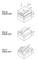
- a Y-branch optical waveguide device 1 is manufactured through processes shown in FIGS. 1A through 1G.
- FIG. 1H shows the completed Y-branch optical waveguide device 1.
- Z1-Z2, X1-X2, and Y1-Y2 indicate the directions of length, width, and thickness (height), respectively, of the Y-branch optical waveguide device 1.
- the Y-branch optical waveguide device 1 includes a Y-branch optical waveguide 2 made of a polymer resin material and a silicon substrate 3.
- the Y-branch optical waveguide 2 is formed on the upper surface of the silicon substrate 3.
- the Y-branch optical waveguide 2 includes a core 4 made of a polymer resin material such as a fluorinated polyimide resin and lower and upper clad layers 5 and 6 surrounding the core 4.
- the lower and upper clad layers 5 and 6 are also made of a fluorinated polyimide resin.
- the core 4, which has a Y-letter shape, includes an entrance-side core 4a and two branch cores 4b and 4c that branch off therefrom. In FIG. 1H, the core 4 is shown with solid lines for convenience of description.
- a fluorinated polyimide resin having a refractive index of n1 is applied on the surface of the silicon substrate 3 so that the lower clad layer 5 is formed.
- a fluorinated polyimide resin having a refractive index of n2 (> n1) is applied on the lower clad layer 5 so that a core layer 10 is formed.
- photoresist including silicon is applied on the core layer 10 so that a resist layer 11 is formed.
- a mask member 20 includes a quartz plate 21 and a Y-shaped mask pattern 22 of a chromium film formed on the lower surface of the quartz plate 21.
- the mask pattern 22 is shown with solid lines for convenience of description.
- the mask member 20 is adhered onto the resist layer 11, and is exposed to ultraviolet radiation 25 so as to develop the resist layer 11.
- a resist mask 12 for dry etching with a reactive ion etching (RIE) apparatus is formed.
- RIE dry etching is performed so that the Y-shaped core 4 is formed as shown in FIG. 1F.
- the core 4 is formed so that both side surfaces (the X1-side and X2-side surfaces) thereof are perpendicular to the upper surface of the silicon substrate 3.
- the resist mask 12 is removed.
- a fluorinated polyimide resin having the refractive index of n1 is applied so that the upper clad layer 6 is formed to cover the core 4.
- the Y-branch optical waveguide device 1 shown in FIG. 1H is manufactured.
- Such an optical waveguide manufacturing method is disclosed in Japanese Laid-Open Patent Application No. 7-92338.
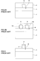
- FIGS. 2A and 2B are cross-sectional views of the Y-branch optical waveguide device 1 of FIG. 1H taken along the line IIA-IIA and the line IIB-IIB, respectively.
- optical fibers 100 are indicated by two-dot chain lines for convenience of description.
- the end of the core 4 (the branch core 4c) is offset with respect to the center of the end of the corresponding optical fiber 100 as shown in FIG. 2B. This causes a problem in that part of the light propagated through the branch core 4c is prevented from entering the optical fiber 100 at the connection of the Y-branch optical waveguide device 1 and the optical fiber 100, thus causing optical loss.
- FIG. 3 is a cross-sectional view of the structure of FIG. 1F taken along the line III-III.
- a more specific object of the present invention is to provide a branch optical waveguide device in which the distortion of a core cross section is eliminated by preventing formation of a crack in a dry etching process using an RIE apparatus.
- an optical waveguide device including a first clad layer on a substrate, the first clad layer being formed of a polymer resin material, a core on the first clad layer, the core being formed of a polymer resin material, and a second clad layer covering the core, the second clad layer being formed of a polymer resin material, wherein the core surrounded by the first and second clad layers forms an optical waveguide, the optical waveguide device characterized in that: the core has first and second opposing surfaces, the first surface facing the first clad layer and the second surface facing away from the first clad layer; and the core is shaped so that a dimension of the first surface is greater than a dimension of the second surface in a cross section of the core.
- the core is shaped so that the dimension of the lower surface thereof is greater than the dimension of the upper surface thereof in a cross section of the core. This prevents formation of a crack in a dry etching process with a reactive ion etching apparatus, thus preventing the cross section of the core perpendicular to the optical axis of the core from being distorted.
- FIG. 4 is perspective view of a Y-branch optical waveguide device 41 according to a first embodiment of the present invention.
- Z1-Z2, X1-X2, and Y1-Y2 indicate the directions of length, width, and thickness (height), respectively, of the Y-branch optical waveguide device 41.
- the Y-branch optical waveguide device 41 includes a Y-branch optical waveguide 42 made of a polymer resin material and a silicon substrate 43.
- the Y-branch optical waveguide 42 is formed on the upper surface of the silicon substrate 43.
- the Y-branch optical waveguide 42 includes a core 44 made of, for instance, a fluorinated polyimide resin having a refractive index of n2 and lower and upper clad layers 45 and 46 surrounding the core 44.
- the lower and upper clad layers 45 and 46 are made of a fluorinated polyimide resin having a refractive index of n1 ( ⁇ n2).
- the core 44 which has a Y-letter shape, includes an entrance-side core 44a and two branch cores 44b and 44c that branch off therefrom. In FIG. 4, the core 44 is shown with solid lines for convenience of description.
- the entrance-side core 44a and the branch cores 44b and 44c are fine, each having a width W1 (FIGS.
- a and 5B of approximately 5 ⁇ m and a height H1 (FIG. 4) of approximately 5 ⁇ m, and are for a single mode.
- the distance A between the branch cores 44b and 44c at the Z1 end is approximately 125-250 ⁇ m, and is set to the diameter of an optical fiber.
- a branch angle ⁇ 1 is set to 0.5-3°, which is an angle at which light can be divided equally.
- each of the entrance-side core 44a and the branch cores 44b and 44c has a cross section having side surfaces 50 flaring at the bottom. That is, the entrance-side core 44a and the branch cores 44b and 44c are shaped so that the width W2 of their lower surface 51 is greater than the width W1 of their upper surface 52.
- FIGS. 5A and 5B are cross-sectional views of the Y-branch optical waveguide device 41 of FIG. 4 taken along the line VA-VA and the line VB-VB, respectively. In FIG. 5B, the optical fibers 100 are indicated by two-dot chain lines for convenience of description.
- each of the entrance-side core 44a and the branch cores 44b and 44c includes no distortion. Accordingly, light that enters the entrance-side core 44a is distributed evenly between the branch cores 44b and 44c, thus ensuring evenness of branching.
- a Y-branch optical waveguide device module formed by connecting optical fibers to the Y-branch optical waveguide device 41 by adhesion
- the ends of the core 44 are substantially aligned with the ends of the optical fibers 100 as shown in FIG. 5B.
- light propagated through the branch cores 44b and 44c enters the optical fibers 100 satisfactorily. Accordingly, optical loss at the connection of the Y-branch optical waveguide device 41 and the optical fibers 100 can be prevented, thus resulting in good optical characteristics.
- the Y-branch optical waveguide device 41 is manufactured through processes shown in FIGS. 6A through 6G.
- the processes are equal to those shown in FIGS. 1A through 1G except that a condition of the dry etching process shown in FIG. 6F using an RIE apparatus is changed.
- FIG. 6F The RIE process shown in FIG. 6F was performed with oxygen pressure inside a chamber 61 of an RIE apparatus 60 shown in FIG. 7 being set to a value causing the reactive ion etching to be isotropic etching, for instance, 5 Pa, which is approximately 10 times its normal value of 0.6 Pa.
- the RIE apparatus 60 includes an upper electrode 62 and a lower electrode 63.
- FIGS. 8A and 8B are cross-sectional views of the structure of FIG. 6F taken along the line VIIIA-VIIIA and the line VIIIB-VIIIB, respectively.
- the inventor of the present invention observed each core on the wafer after the RIE process, and confirmed that no crack is formed in the portions of the lower clad layer 45 which portions oppose the lower edges of the side surfaces 50 of the entrance-side core 44a and the branch cores 44b and 44c.
- the inventor of the present invention observed the completed Y-branch optical waveguide devices 41, and confirmed that none of the entrance-side core 44a and the branch cores 44b and 44c has a distorted cross section as shown in FIGS. 2A and 2B in any of the completed Y-branch optical waveguide devices 41.
- the Y-branch optical waveguide device 41 can be formed stably with high quality and little variation in quality through the above-described manufacturing process.
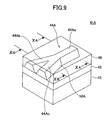
- FIG. 9 is a perspective view of a Y-branch optical waveguide device 41A according to a second embodiment of the present invention.
- the Y-branch optical waveguide device 41A is equal to the Y-branch optical waveguide device 41 of the first embodiment except for a core 44A.
- Each of an entrance-side core 44Aa and two branch cores 44Ab and 44Ac that branch off therefrom has sloping side surfaces 50A so as to have a trapezoidal cross section as shown also in FIGS. 10A and 10B.
- the core 44A is also formed by performing RIE under a predetermined condition. In FIG. 9, the core 44A is shown with solid lines for convenience of description.
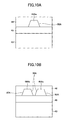
- FIGS. 10A and 10B are cross-sectional views of the Y-branch optical waveguide device 41A of FIG. 9 taken along the line XA-XA and the line XB-XB, respectively.
- the Y-branch optical waveguide device 41A has an improved branching characteristic.
- a Y-branch optical waveguide device module formed by connecting optical fibers to the Y-branch optical waveguide device 41A by adhesion, optical loss at the connection is prevented, thus resulting in improved optical characteristics.
- the configuration according to the present invention where the width of a core cross-sectional shape is greater on the lower surface side than on the upper surface side, is applicable not only to Y-branch optical waveguide devices but also to devices with an optical waveguide having a shape other than a Y-letter shape and devices with an optical waveguide with no branching function, and the same effects as described above can be produced.
- the core is shaped so that the dimension of the lower surface thereof is greater than the dimension of the upper surface thereof in a cross section of the core. This prevents formation of a crack in a dry etching process with a reactive ion etching apparatus, thus preventing the cross section of the core perpendicular to the optical axis of the core from being distorted.
Landscapes
- Physics & Mathematics (AREA)
- Engineering & Computer Science (AREA)
- Microelectronics & Electronic Packaging (AREA)
- General Physics & Mathematics (AREA)
- Optics & Photonics (AREA)
- Optical Integrated Circuits (AREA)
Applications Claiming Priority (2)
| Application Number | Priority Date | Filing Date | Title |
|---|---|---|---|
| JP2003397471 | 2003-11-27 | ||
| JP2003397471A JP2005157090A (ja) | 2003-11-27 | 2003-11-27 | 光導波路デバイス |
Publications (2)
| Publication Number | Publication Date |
|---|---|
| EP1536254A1 true EP1536254A1 (de) | 2005-06-01 |
| EP1536254B1 EP1536254B1 (de) | 2009-03-25 |
Family
ID=34463839
Family Applications (1)
| Application Number | Title | Priority Date | Filing Date |
|---|---|---|---|
| EP04254980A Expired - Lifetime EP1536254B1 (de) | 2003-11-27 | 2004-08-19 | Optische Wellenleitervorrichtung |
Country Status (5)
| Country | Link |
|---|---|
| US (1) | US7003207B2 (de) |
| EP (1) | EP1536254B1 (de) |
| JP (1) | JP2005157090A (de) |
| CN (1) | CN1621873A (de) |
| DE (1) | DE602004020169D1 (de) |
Families Citing this family (1)
| Publication number | Priority date | Publication date | Assignee | Title |
|---|---|---|---|---|
| JP4318036B2 (ja) * | 2004-02-16 | 2009-08-19 | オムロン株式会社 | 光導波路 |
Citations (3)
| Publication number | Priority date | Publication date | Assignee | Title |
|---|---|---|---|---|
| JPS57155507A (en) * | 1981-03-20 | 1982-09-25 | Fuji Photo Film Co Ltd | Manufacture of high density photoconductive sheet |
| US20030026569A1 (en) * | 2001-05-01 | 2003-02-06 | Louay Eldada | Optimized multi-layer optical waveguiding system |
| EP1336894A2 (de) * | 2002-02-19 | 2003-08-20 | Omron Corporation | Ein optischer Wellenleiter, ein optisches Bauelement und ein optischer Schalter |
Family Cites Families (5)
| Publication number | Priority date | Publication date | Assignee | Title |
|---|---|---|---|---|
| EP0394597A1 (de) * | 1989-04-28 | 1990-10-31 | International Business Machines Corporation | System zum Verfolgen eines Ätzprozesses in einer RIE-Vorrichtung und dessen Verwendung zur Herstellung reproduzierbarer Strukturen hoher Auflösung |
| US5138687A (en) * | 1989-09-26 | 1992-08-11 | Omron Corporation | Rib optical waveguide and method of manufacturing the same |
| JP3327356B2 (ja) | 1993-03-18 | 2002-09-24 | 日本電信電話株式会社 | フッ素化ポリイミド光導波路及びその製造方法 |
| EP0754309A1 (de) * | 1995-02-07 | 1997-01-22 | LDT GmbH & Co. Laser-Display-Technologie KG | Streifen-wellenleiter und verwendungen |
| TWI243288B (en) * | 2002-11-26 | 2005-11-11 | Asml Netherlands Bv | Method of fabricating an optical element, lithographic apparatus and semiconductor device manufacturing method |
-
2003
- 2003-11-27 JP JP2003397471A patent/JP2005157090A/ja active Pending
-
2004
- 2004-08-17 US US10/919,629 patent/US7003207B2/en not_active Expired - Fee Related
- 2004-08-19 DE DE602004020169T patent/DE602004020169D1/de not_active Expired - Fee Related
- 2004-08-19 EP EP04254980A patent/EP1536254B1/de not_active Expired - Lifetime
- 2004-08-31 CN CN200410074049.8A patent/CN1621873A/zh active Pending
Patent Citations (3)
| Publication number | Priority date | Publication date | Assignee | Title |
|---|---|---|---|---|
| JPS57155507A (en) * | 1981-03-20 | 1982-09-25 | Fuji Photo Film Co Ltd | Manufacture of high density photoconductive sheet |
| US20030026569A1 (en) * | 2001-05-01 | 2003-02-06 | Louay Eldada | Optimized multi-layer optical waveguiding system |
| EP1336894A2 (de) * | 2002-02-19 | 2003-08-20 | Omron Corporation | Ein optischer Wellenleiter, ein optisches Bauelement und ein optischer Schalter |
Non-Patent Citations (2)
| Title |
|---|
| KAGAMI M ET AL: "FABRICATION OF LARGE-CORE, HIGH- OPTICAL WAVEGUIDES IN POLYMERS", APPLIED OPTICS, OPTICAL SOCIETY OF AMERICA,WASHINGTON, US, vol. 34, no. 6, 20 February 1995 (1995-02-20), pages 1041 - 1046, XP000490005, ISSN: 0003-6935 * |
| PATENT ABSTRACTS OF JAPAN vol. 0062, no. 58 (P - 163) 17 December 1982 (1982-12-17) * |
Also Published As
| Publication number | Publication date |
|---|---|
| DE602004020169D1 (de) | 2009-05-07 |
| CN1621873A (zh) | 2005-06-01 |
| JP2005157090A (ja) | 2005-06-16 |
| US7003207B2 (en) | 2006-02-21 |
| US20050117865A1 (en) | 2005-06-02 |
| EP1536254B1 (de) | 2009-03-25 |
Similar Documents
| Publication | Publication Date | Title |
|---|---|---|
| US7184630B2 (en) | Optical coupling module with self-aligned etched grooves and method for fabricating the same | |
| US7546007B2 (en) | Broadband optical via | |
| US8126301B2 (en) | Optical waveguide and method for producing the same | |
| US8447152B2 (en) | Waveguide coupling device with properties of forward and backward coupling as well as manufacturing method thereof | |
| US20090003770A1 (en) | Vertical optical coupling structure | |
| JP4377195B2 (ja) | 光モジュールの製造方法 | |
| CN112394446A (zh) | 端面耦合器及其制作方法、端面耦合方法 | |
| CN112630886A (zh) | 端面耦合器及其制造方法 | |
| US20050213913A1 (en) | Optical waveguide circuit and method for fabricating the same | |
| JP2017173710A (ja) | 光ファイバ搭載光集積回路装置 | |
| JP6270936B1 (ja) | 光導波路素子 | |
| EP1536254B1 (de) | Optische Wellenleitervorrichtung | |
| CN100470278C (zh) | 光分路单元及其制造方法 | |
| JP2001281479A (ja) | 高分子光導波路素子およびその製造方法 | |
| JPH10288717A (ja) | V溝付光導波路基板の製造方法及びその製法により製造されたv溝付光導波路基板 | |
| JP4306678B2 (ja) | 光導波路装置の製造方法 | |
| US12072529B2 (en) | Optical waveguides and methods for producing | |
| JPH0886926A (ja) | 光分岐ディバイス | |
| EP1536253A1 (de) | Verfahren zur Herstellung eines verzweigten optischen Wellenleiters | |
| WO2003091776A1 (fr) | Guide d'ondes optique en resine et son procede de fabrication | |
| JP6029703B2 (ja) | 光導波路素子 | |
| US7450803B2 (en) | Optical waveguide | |
| CN119376014B (zh) | 一种多维楔形模斑转换器及其制造方法 | |
| JPH11264912A (ja) | 光配線 | |
| US6921491B2 (en) | Method for forming a groove and method for manufacturing an optical waveguide element |
Legal Events
| Date | Code | Title | Description |
|---|---|---|---|
| PUAI | Public reference made under article 153(3) epc to a published international application that has entered the european phase |
Free format text: ORIGINAL CODE: 0009012 |
|
| 17P | Request for examination filed |
Effective date: 20050314 |
|
| AK | Designated contracting states |
Kind code of ref document: A1 Designated state(s): AT BE BG CH CY CZ DE DK EE ES FI FR GB GR HU IE IT LI LU MC NL PL PT RO SE SI SK TR |
|
| AX | Request for extension of the european patent |
Extension state: AL HR LT LV MK |
|
| AKX | Designation fees paid |
Designated state(s): DE |
|
| 17Q | First examination report despatched |
Effective date: 20051220 |
|
| GRAP | Despatch of communication of intention to grant a patent |
Free format text: ORIGINAL CODE: EPIDOSNIGR1 |
|
| GRAS | Grant fee paid |
Free format text: ORIGINAL CODE: EPIDOSNIGR3 |
|
| GRAA | (expected) grant |
Free format text: ORIGINAL CODE: 0009210 |
|
| AK | Designated contracting states |
Kind code of ref document: B1 Designated state(s): DE |
|
| REF | Corresponds to: |
Ref document number: 602004020169 Country of ref document: DE Date of ref document: 20090507 Kind code of ref document: P |
|
| PLBE | No opposition filed within time limit |
Free format text: ORIGINAL CODE: 0009261 |
|
| STAA | Information on the status of an ep patent application or granted ep patent |
Free format text: STATUS: NO OPPOSITION FILED WITHIN TIME LIMIT |
|
| 26N | No opposition filed |
Effective date: 20091229 |
|
| PG25 | Lapsed in a contracting state [announced via postgrant information from national office to epo] |
Ref country code: DE Free format text: LAPSE BECAUSE OF NON-PAYMENT OF DUE FEES Effective date: 20100302 |