EP1535879A1 - Mems array, manufacturing method thereof, and mems device manufacturing method based on the same - Google Patents
Mems array, manufacturing method thereof, and mems device manufacturing method based on the same Download PDFInfo
- Publication number
- EP1535879A1 EP1535879A1 EP03760931A EP03760931A EP1535879A1 EP 1535879 A1 EP1535879 A1 EP 1535879A1 EP 03760931 A EP03760931 A EP 03760931A EP 03760931 A EP03760931 A EP 03760931A EP 1535879 A1 EP1535879 A1 EP 1535879A1
- Authority
- EP
- European Patent Office
- Prior art keywords
- switches
- elements
- mems array
- mems
- interconnect layer
- Prior art date
- Legal status (The legal status is an assumption and is not a legal conclusion. Google has not performed a legal analysis and makes no representation as to the accuracy of the status listed.)
- Withdrawn
Links
Images









Classifications
-
- H—ELECTRICITY
- H10—SEMICONDUCTOR DEVICES; ELECTRIC SOLID-STATE DEVICES NOT OTHERWISE PROVIDED FOR
- H10D—INORGANIC ELECTRIC SEMICONDUCTOR DEVICES
- H10D88/00—Three-dimensional [3D] integrated devices
-
- H—ELECTRICITY
- H10—SEMICONDUCTOR DEVICES; ELECTRIC SOLID-STATE DEVICES NOT OTHERWISE PROVIDED FOR
- H10D—INORGANIC ELECTRIC SEMICONDUCTOR DEVICES
- H10D84/00—Integrated devices formed in or on semiconductor substrates that comprise only semiconducting layers, e.g. on Si wafers or on GaAs-on-Si wafers
Definitions
- the present invention relates to technology utilizing a MEMS (Micro Electro-Mechanical System), more particularly relates to a micromachine and MEMS array provided with a plurality of circuit elements and switches.
- MEMS Micro Electro-Mechanical System
- MEMS's integrally form not only electronic circuits, but also different elements such as sensors and actuators on an Si or other substrate to impart sophisticated functions, so hold the promise of great growth.
- technology for producing MEMS devices (1) mounting sensors and other individual elements made using MEMS technology on substrates and (2) producing individual specialized MEMS circuits have been known.
- the present invention in consideration of the above problems, has as its object to provide a programmable MEMS array enabling a reduction of size and enabling the development time and development costs to be slashed and to provide a method of producing a MEMS device using the same.
- the present invention achieves this object by providing a MEMS array comprised of a plurality of elements and switches for connecting the elements arranged on a substrate and enabling the elements to be freely connected.
- the MEMS array of the present invention is provided with a plurality of elements in at least one layer and provided with the switches in another layer.
- the switches of the MEMS array of the present invention may be constituted by transistors or may be constituted by mechanical switches.
- a MEMS device based on the MEMS array. That is, a MEMS device is produced by the step of determining the connection states of the switches of the MEMS array to form a desired circuit, then interconnecting elements in accordance with the connection states of the switches.
- a freely connectable programmable MEMS array of a first embodiment of the present invention will be explained with reference to FIGS. 1 to 6.
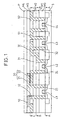
- FIG. 1 is a partial cross-sectional view of a freely connectable MEMS array of this embodiment
- FIG. 2 is a schematic view of a MEMS array of the present invention overall
- FIG. 3 is a view of an equivalent circuit of this embodiment whose cross-section is shown in FIG. 1.
- the freely connectable MEMS array of the present invention is comprised of a for example 10 mm 2 Si chip formed with about 300,000 freely connectable circuit elements utilizing the semiconductor wafer process.
- a region T of 10 ⁇ m square is provided with three LCR circuits forming a single circuit.
- FIG. 1 shows a cross-section of the LCR circuit shown by the bold line in the equivalent circuit shown in FIG. 3.
- the MEMS array of this embodiment is comprised of a substrate S, transistors 41 to 44 with source and drain regions formed on it, interconnect layers M0 to M4 formed over that, and a passivation layer P provided over that.
- An LCR circuit is comprised a resistor 10, a capacitor 20, a coil 30, and their via interconnects formed in interconnect layers M0 to M1 to be connectable in series by switches 41 to 44 comprised of four transistors (FETs) formed on the substrate S.
- adjoining elements of the three LCRs can be connected by the large number of switches including the switches 41 to 44.
- the bottommost part is provided with a switch 45 arranged in parallel with the elements so that the elements can be bypassed. Any combination of the elements is possible.
- the MEMS array comprised of the LCR circuits of the present embodiment is comprised of a plurality of resistors, capacitors, and coils regularly arranged in a planar form (two-dimensionally).
- the elements can be freely connected through switches.
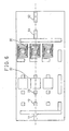
- FIG. 4 is a top view of the substrate S cut along the line A-A of FIG. 1
- FIG. 5 is a top view of the interconnect layer M1 cut along the line B-B
- FIG. 6 is a top view of the interconnect layer M3 cut long the line C-C.
- FIG. 4 shows the general arrangement of the sources and drains of the transistors forming the switches provided on the substrate S.
- the sources and drains arranged corresponding to the switches 41 to 44 are shown by the same reference numerals.
- the interconnect layer M0 is an interconnect layer formed with gate electrodes of transistors and formed with some of the interconnects to the sources and drains.
- the interconnects include the interconnect 12 to the resistor 10 for the switch 41, the interconnect 23 to the top electrode 21 of the capacitor 20, the interconnect 24 to the bottom electrode 22 of the capacitor 20 for the switch 42, the interconnects 31 and 32 for the coil 30, and the interconnects 51 and 52 for the switches 43 and 44.
- the interconnect layer M1 is shown in FIG. 5 and is provided with one interconnect part 12 of the resistor 10, the interconnect 23 to the top electrode of the capacitor 20, the interconnect 24 to the bottom electrode 22, the interconnects 31 and 32 of the coil 30, and the interconnects 51 and 52 of the switches 43 and 44.
- the interconnects 12, 23, 24, 31, and 32 also serve as interconnects leading to the switches for parallel connection.
- the interconnect layer M2 is an interconnect layer on which some of the interconnects between the elements and switches are formed.
- the interconnects are similar to those of the interconnect layer M0, so their explanations will be omitted.
- the interconnect layer M3 is shown in FIG. 6 and is provided with interconnect parts 11 and 12 of the resistor 10, the interconnect 23 to the top electrode of the capacitor 20, the bottom electrode 22 of the capacitor 20, the coil 30, and the interconnect parts 51 and 52 to the switches 43 and 44.
- the interconnects 11 and 51 serve also an interconnects for parallel connection.
- the interconnect at the bottom end (no reference numeral) is a bypass interconnect.
- the interconnect layer M4 is provided with the resistor 10 and provided with the top electrode 21 of the capacitor 20.
- the topmost part is provided with a passivation layer P.
- this layer is just an example for explanation.
- the number of the layers and other aspects of the configuration are not limited.
- the types of the elements are also not limited to LCRs.
- the elements need only be ones forming a high frequency filter circuit or other desired electrical or electronic circuit. Their shapes, arrangements, etc. may be suitably selected.
- the method of production of the MEMS array of the present embodiment is similar to an Si wafer process and comprises forming a plurality of interconnect layers on a substrate 1 formed with transistor switches.
- a substrate 1 formed with transistor switches For example, when forming passive elements as well, it is possible to form suitable shapes according to the materials of the conductor layers and otherwise use suitable known wafer processes for production.
- the MEMS array of the present embodiment is comprised of a plurality of circuit elements able to be suitably connected through switches, so by just determining the on/off states of the switches in accordance with the design of the designer, it is possible to freely form a desired circuit.
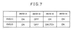
- FIG. 7 is a view of the on/off states of the switches 41 to 44 in a circuit formed using the MEMS array of FIG. 1.
- FIG. 7 shows the result when using a MEMS array according to the present invention and selecting the on/off states of the switches to form a desired circuit.
- the state (1) is an example of a static circuit with no switching during circuit operation
- the state (2) is an example of a dynamic circuit with some switching during circuit operation.
- the switch 41 In the state (1) of the switches, the switch 41 is on, the switch 42 is off, the switch 43 is on, and the switch 44 is on. This state does not change during the circuit operation. Therefore, the constantly on switches have to be supplied with gate voltage to maintain the on state. This is not economical if considering the power consumption.
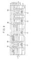
- the substrate S is not formed with any transistor switches. These are replaced by an interconnect layer M0' corresponding to the on/off state of the switches. That is, when the switches 41, 43, and 44 are on, the interconnects 60 are formed for connection (short-circuiting), while when the switch 42 is off, no interconnects are formed (open). By doing this, it is possible to reduce the power and produce a device almost completely free of malfunctions.
- the production process of a MEMS array can be utilized. Further, the step of formation of the transistors can be eliminated and a low cost substrate S can be used, so a mass production device can be made at a low cost.
- the state (2) of the switches is the same as the state (1) except for the point that the switch 43 is used as a changeable switch. This differs from the case of the state (1) in that it does not allow all of the switches to be replaced with short-circuit/open states of interconnects.
- the interconnects 60 may be provided to short-circuit the switches 41 and 44 (short-circuiting).
- the circuit is broken (open) without forming an interconnect to prevent voltage from being supplied to the gate of the transistor.
- it is sufficient to provide a via to connect the top and bottom so as to maintain the existing interconnect.
- the switches connecting adjoining elements were comprised of transistors, but this embodiment forms these switches by mechanical switches, that is, electrostatic switches. Operating the electrostatic switches requires drive transistors, but mechanical switches do not cause changes in the circuit characteristics when turned on and off compared with transistor switches, so are advantageous when using a MEMS array to form a circuit.
- FIG. 10 is a partial cross-sectional view of the part of the MEMS array of the present embodiment omitting the substrate. Components having the same functions as in the first embodiment are assigned the same reference notations.
- FIG. 10 shows the interconnect layers M0 to M4 and the passivation layer P on the substrate. Note that the layers are provided between them with Cu cap layers C comprised of silicon nitride etc. These prevent the copper of the interconnect layers from diffusing in the insulating films and causing device defects.
- the outermost layer is provided with electrostatic switches 41' to 43' having cantilever type movable parts.
- the switch drive parts 71 to 73 are connected through interconnect vias 74 to 76 to transistors provided on the not shown substrate.
- the electrostatic switches 41' to 43' close the contacts when the switch drive parts 71 to 73 are given a predetermined voltage and the corresponding movable pieces are attracted. While not shown, a cover may also be provided for protecting the switches and preventing entry of dust.
- q resistor 10, capacitor 20, and coil are formed.
- the resistor 10, switch 41', capacitor 20, switch 42', coil 30, and switch 43' can be serially connected. These are designed to be connectable to other adjoining elements not shown in the cross-sectional view of FIG. 10 through the switches. The elements can be freely connected.
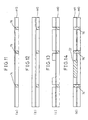
- FIGS. 11 to 14 show steps (a) to (d) up to formation of the interconnect layer M1.
- transistors for driving the static switches are formed on a not shown substrate, then vias 74 to 76 for the interconnects are provided to form the interconnect layer M0.
- an insulating film is formed, at step (c) of FIG. 13, the insulating film is etched for forming the bottom electrode 22 of the capacitor 20 and vias, and at step (d) of FIG. 14, the capacitor bottom electrode is formed and the vias are connected to form the interconnect layer M1.
- FIGS. 15 to 17 show the steps (e) to (g) up to formation of the vias of the interconnect layer M2.
- an insulating film is formed
- the insulating film is etched to form the vias
- the vias 74 to 76 of the interconnect layer M2 are formed.
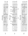
- the etching before forming the capacitor top electrode and coil of the interconnect layer M2 is shown. This is not formed simultaneously with the vias 74 to 76 of the previous step because it is necessary to leave the Cu cap layer for use as the dielectric of the capacitor.
- step (i) of FIG. 19 the capacitor top electrode 21 and coil 30 are formed.
- interconnect layer M3 along with the switch drive interconnects 74 to 76, interconnects 23 and 24 to the capacitor 20 and interconnects 31 and 32 to the coil 30 are formed.
- the interconnect layer M4 is formed. That is, at step (m) of FIG. 23, an insulating film is formed, at step (n) of FIG. 24, the input/output parts of the resistor 10 (FIG. 10), capacitor 20, and coil 30 and the parts for forming the switch drive electrodes are etched, and at step (o) of FIG. 25, the input/output parts 11 and 12 of the resistor 10 (FIG. 10), the input/output parts 25 and 26 of the capacitor 20, the input/output parts 33 and 34 of the coil 30, the switch drive electrodes 71 to 73, etc. are formed.
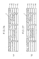
- FIGS. 26 to 29 show the steps of formation of the resistor 10.
- a Cu cap layer C is formed at step (p) of FIG. 26.
- the Cu cap layer C is etched to form a resistance thin film forming part.
- a resistance thin film R is formed over the entire surface.
- the film is etched leaving only the part for use as the resistor to thereby form the resistor 10.
- FIGS. 30 to 35 show steps of forming switches from the formation of the protective passivation film P.
- a protective passivation film P is formed over the entire surface.
- this is etched to provide the tops of the switches 41' to 43'.
- the surface is further etched for providing the connections of the switches 41' to 43'.
- the switches are made, at step (x) of FIG. 34, the tops of the switches 41' to 43' are released, and at step (y) of FIG. 35, the bottoms of the switches 41' to 43' are released to complete the switches.
- the resistor 10, capacitor 20, and coil 30 can be connected serially through the switches 41' to 43'.
- the point of formation of a large number of RCL series circuits in a planar (two-dimensional) form is the same as in the first embodiment. It is also possible to select the on/off states of the switches to form a desired circuit.
- the present embodiment requires transistor switches for driving the electrostatic switches, so has the increased step of providing electrostatic switches compared with the first embodiment, but in addition to the advantage of stabilization of the circuit characteristics by using electrostatic switches, there are the following advantages in the production of static circuit or dynamic circuit MEMS devices.
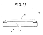
- electrostatic switches provided with cantilever type movable electrodes and turning on by attraction by electrostatic force were used, but it is also possible to use electrostatic switches 90 shown in FIG. 36. These are ones where drive electrodes 91 are supplied with voltage and thereby movable electrodes 92 are attracted by electrostatic force and short-circuited so as to turn off. Further, it is also possible to employ suitable switches other than these.
- electrostatic switches were arranged above the interconnect layer, but may also be provided in an interconnect layer.
- the plurality of elements may also be arranged three-dimensionally and may also be arranged randomly.
- the substrate of the MEMS array of the present invention may also carry other semiconductor circuits for signal processing. Further, the semiconductor circuits arranged on the semiconductor substrate may be made three-dimensional in structure as well. Further, the same package where the MEMS device is housed may also house a microprocessor, flash memory, EEPROM, or other semiconductor circuit or device suitable for signal processing to obtain a final product. By adding such other semiconductor circuits or devices, the freedom of circuit configuration is enhanced and a desired high performance MEMS device can be obtained.
- the freely connectable MEMS array of the present invention is programmable and has general applicability, so no special mask or special process is required.
- connection states By just designating the connection states, a desired MEMS device can be developed at a low cost. Changes to the prototype are also possible by just resetting the on/off states of the switches. Further, the on/off parts of the switches can be replaced by short-circuit/open states of interconnects, so shortening of the delivery and reduction of the power consumption in semicustom made products become possible. Further, if testing the MEMS array in advance, since the circuits are almost the same, the tests after production of the MEMS devices will almost never find that the specifications are not met and the certification time of devices can therefore be shortened.
Landscapes
- Semiconductor Integrated Circuits (AREA)
- Micromachines (AREA)
- Design And Manufacture Of Integrated Circuits (AREA)
Abstract
Description
Claims (23)
- A MEMS array characterized by being provided with a plurality of elements and switches for connecting said elements and by enabling the elements to be freely interconnected.
- A MEMS array as set forth in claim 1, wherein the switches connecting the elements are semiconductor switches.
- A MEMS array as set forth in claim 1, wherein the switches connecting the elements are mechanical switches.
- A MEMS array as set forth in claim 1, provided with a substrate and an interconnect layer, said substrate being formed with said switches, said interconnect layer provided with a plurality of elements connected through said switches.
- A MEMS array as set forth in claim 4, wherein said substrate is provided with drive parts for driving said switches.
- A MEMS array as set forth in claim 5, wherein said substrate is further provided with semiconductor circuits for signal processing.
- A MEMS array as set forth in claim 6, wherein said semiconductor circuits have three-dimensional structures.
- A MEMS array as set forth in claim 1, provided with a substrate and interconnect layer, said interconnect layer provided with a plurality of elements and switches for connecting the elements.
- A MEMS array as set forth in claim 8, wherein said substrate is provided with drive parts for driving said switches.
- A MEMS array as set forth in claim 9, wherein said substrate is provided with semiconductor circuits for signal processing.
- A MEMS array as set forth in claim 10, wherein said semiconductor circuits have three-dimensional structures.
- A MEMS array as set forth in claim 1, provided with a substrate and interconnect layer, said interconnect layer provided with a plurality of elements, switches for connecting said elements being provided on the interconnect layer.
- A MEMS array as set forth in claim 12, wherein said substrate is provided with drive parts for driving said switches.
- A MEMS array as set forth in claim 13, wherein said substrate is provided with semiconductor circuits for signal processing.
- A MEMS array as set forth in claim 14, wherein said semiconductor circuits have three-dimensional structures.
- A MEMS array as set forth in claim 1, wherein the same package packages semiconductor circuits built in.
- A method of production of a MEMS array providing an interconnect layer on a substrate,
said method of production of a MEMS array characterized by having:a step of forming a plurality of switches in said substrate anda step of forming a plurality of elements connected through said plurality of switches in said interconnect layer. - A method of production of a MEMS array providing an interconnect layer on a substrate,
said method of production of a MEMS array characterized by having:a step of forming a plurality of elements in said interconnect layer anda step of providing a plurality of switches for connecting said plurality of elements on said interconnect layer. - A method of production of a MEMS array providing an interconnect layer on a substrate,
said method of production of a MEMS array characterized by having:a step of forming switch drive parts on said substrate,a step of forming a plurality of elements in said interconnect layer, anda step of providing a plurality of switches for connecting said plurality of elements on said interconnect layer. - A method of production of a MEMS device having a plurality of elements of the same arrangement as a MEMS array provided with a plurality of elements and switches for connecting said elements,
said method of production of a MEMS device characterized by having:a step of determining connection states of switches of said MEMS array anda step of forming an interconnect layer connecting elements in accordance with the connection states of said switches. - A method of production of a MEMS device having a plurality of elements of the same arrangement as a MEMS array provided with a plurality of elements and switches for connecting said elements,
said method of production of a MEMS device characterized by having:a step of determining connection states of switches of said MEMS array,a step of forming an interconnect layer connecting elements in accordance with the connection states of said switches on the substrate of said MEMS device, anda step of forming a plurality of elements of the same arrangement as the MEMS array on said interconnect layer. - A method of production of a MEMS device having a plurality of elements of the same arrangement as a MEMS array provided with a plurality of elements and switches for connecting said elements,
said method of production of a MEMS device characterized by having:a step of determining connection states of switches of said MEMS array,a step of providing switches in the substrate of the MEMS device,a step of providing an additional interconnect layer for short-circuiting, opening, or connecting said switches in accordance with the connection states of said switches on the substrate of the MEMS device, anda step of providing an interconnect layer arranging a plurality of elements of the same arrangement as said MEMS array on said additional interconnect layer. - A method of production of a MEMS device having a plurality of elements of the same arrangement as a MEMS array provided with a plurality of elements and switches for connecting said elements,
said method of production of a MEMS device characterized by having:a step of determining connection states of switches of said MEMS array,a step of forming an interconnect layer providing a plurality of elements of the same arrangement as said MEMS array, anda step of selectively forming switches and interconnects on said interconnect layer based on the connection states of said switches.
Applications Claiming Priority (3)
| Application Number | Priority Date | Filing Date | Title |
|---|---|---|---|
| JP2002181965 | 2002-06-21 | ||
| JP2002181965A JP3955241B2 (en) | 2002-06-21 | 2002-06-21 | MEMS array, manufacturing method thereof, and manufacturing method of MEMS device based thereon |
| PCT/JP2003/007891 WO2004000719A1 (en) | 2002-06-21 | 2003-06-20 | Mems array, manufacturing method thereof, and mems device manufacturing method based on the same |
Publications (2)
| Publication Number | Publication Date |
|---|---|
| EP1535879A1 true EP1535879A1 (en) | 2005-06-01 |
| EP1535879A4 EP1535879A4 (en) | 2006-06-07 |
Family
ID=29996635
Family Applications (1)
| Application Number | Title | Priority Date | Filing Date |
|---|---|---|---|
| EP03760931A Withdrawn EP1535879A4 (en) | 2002-06-21 | 2003-06-20 | MEMS NETWORK, METHOD FOR MANUFACTURING SAME, AND METHOD FOR MANUFACTURING CORRESPONDING MEMS DEVICE |
Country Status (6)
| Country | Link |
|---|---|
| US (1) | US20050156259A1 (en) |
| EP (1) | EP1535879A4 (en) |
| JP (1) | JP3955241B2 (en) |
| CN (1) | CN1308221C (en) |
| AU (1) | AU2003244114A1 (en) |
| WO (1) | WO2004000719A1 (en) |
Families Citing this family (6)
| Publication number | Priority date | Publication date | Assignee | Title |
|---|---|---|---|---|
| JP4713849B2 (en) * | 2004-05-31 | 2011-06-29 | 株式会社日立ハイテクノロジーズ | Manufacturing method of multilayer wiring board |
| KR100621827B1 (en) | 2005-08-08 | 2006-09-11 | 한국과학기술원 | Nonvolatile Mechanical Memory |
| US7605466B2 (en) * | 2007-10-15 | 2009-10-20 | General Electric Company | Sealed wafer packaging of microelectromechanical systems |
| US7915696B2 (en) * | 2007-10-24 | 2011-03-29 | General Electric Company | Electrical connection through a substrate to a microelectromechanical device |
| CN102180435B (en) * | 2011-03-15 | 2012-10-10 | 迈尔森电子(天津)有限公司 | Integrated MEMS device and method of forming the same |
| FR3077163B1 (en) * | 2018-01-22 | 2021-08-27 | Soitec Silicon On Insulator | DESIGN AND MANUFACTURING METHODS OF A DEVICE INCLUDING A NETWORK OF MICRO-FACTORY ELEMENTS, A DEVICE OBTAINED AS A RESULT OF SUCH METHODS |
Family Cites Families (9)
| Publication number | Priority date | Publication date | Assignee | Title |
|---|---|---|---|---|
| JP2874550B2 (en) * | 1994-04-21 | 1999-03-24 | 日本電気株式会社 | Semiconductor integrated circuit device |
| US5825068A (en) * | 1997-03-17 | 1998-10-20 | Integrated Device Technology, Inc. | Integrated circuits that include a barrier layer reducing hydrogen diffusion into a polysilicon resistor |
| KR100561792B1 (en) * | 1997-08-05 | 2006-03-21 | 코닌클리케 필립스 일렉트로닉스 엔.브이. | Method of manufacturing a plurality of electronic devices |
| US6020848A (en) * | 1998-01-27 | 2000-02-01 | The Boeing Company | Monolithic microwave integrated circuits for use in low-cost dual polarization phased-array antennas |
| US6287951B1 (en) * | 1998-12-07 | 2001-09-11 | Motorola Inc. | Process for forming a combination hardmask and antireflective layer |
| JP3221420B2 (en) * | 1998-12-18 | 2001-10-22 | 日本電気株式会社 | Semiconductor high frequency integrated circuit and method of manufacturing the same |
| EP1093143A1 (en) * | 1999-10-15 | 2001-04-18 | Lucent Technologies Inc. | Flip-chip bonded micro-relay on integrated circuit chip |
| JP3538109B2 (en) * | 2000-03-16 | 2004-06-14 | 日本電気株式会社 | Micro machine switch |
| US6399997B1 (en) * | 2000-08-01 | 2002-06-04 | Megic Corporation | High performance system-on-chip using post passivation process and glass substrates |
-
2002
- 2002-06-21 JP JP2002181965A patent/JP3955241B2/en not_active Expired - Fee Related
-
2003
- 2003-06-20 US US10/518,642 patent/US20050156259A1/en not_active Abandoned
- 2003-06-20 WO PCT/JP2003/007891 patent/WO2004000719A1/en not_active Ceased
- 2003-06-20 AU AU2003244114A patent/AU2003244114A1/en not_active Abandoned
- 2003-06-20 EP EP03760931A patent/EP1535879A4/en not_active Withdrawn
- 2003-06-20 CN CNB038196220A patent/CN1308221C/en not_active Expired - Fee Related
Also Published As
| Publication number | Publication date |
|---|---|
| JP3955241B2 (en) | 2007-08-08 |
| JP2004025321A (en) | 2004-01-29 |
| WO2004000719A1 (en) | 2003-12-31 |
| EP1535879A4 (en) | 2006-06-07 |
| CN1675125A (en) | 2005-09-28 |
| US20050156259A1 (en) | 2005-07-21 |
| AU2003244114A1 (en) | 2004-01-06 |
| CN1308221C (en) | 2007-04-04 |
Similar Documents
| Publication | Publication Date | Title |
|---|---|---|
| KR102704554B1 (en) | Architectural design and process for manufacturing monolithic integrated 3D CMOS logic and memory | |
| US8945998B2 (en) | Programmable semiconductor interposer for electronic package and method of forming | |
| US6686768B2 (en) | Electrically-programmable interconnect architecture for easily-configurable stacked circuit arrangements | |
| US6911730B1 (en) | Multi-chip module including embedded transistors within the substrate | |
| US5691209A (en) | Lattice interconnect method and apparatus for manufacturing multi-chip modules | |
| US5721151A (en) | Method of fabricating a gate array integrated circuit including interconnectable macro-arrays | |
| CN109148423B (en) | Semiconductor devices | |
| JP5480382B2 (en) | Antifuse structure and formation method | |
| US20050184375A1 (en) | Electronic device configured as a multichip module, leadframe and panel with leadframe positions | |
| WO2006072142A1 (en) | A reprogrammable integrated circuit | |
| US6281564B1 (en) | Programmable integrated passive devices | |
| US5760428A (en) | Variable width low profile gate array input/output architecture | |
| US20050156259A1 (en) | Mems array, manufacturing method thereof, and mems device manufacturing method based on the same | |
| US20040124538A1 (en) | Multi-layer integrated semiconductor structure | |
| US10714422B2 (en) | Anti-fuse with self aligned via patterning | |
| JP2006100826A (en) | Structure and method for adjusting the resistance value of a resistor of an integrated circuit | |
| EP0650196A2 (en) | Semiconductor integrated circuit device and method of producing the same using master slice approach | |
| KR100732778B1 (en) | MEMS array and manufacturing method thereof, and manufacturing method of MEMS device based thereon | |
| KR20050021999A (en) | Mems array, manufacturing method thereof, and mems device manufacturing method based on the same | |
| US7064427B2 (en) | Buried array capacitor and microelectronic structure incorporating the same | |
| US20060192612A1 (en) | Capacitor reliability for multiple-voltage power supply systems | |
| CN109326576B (en) | interconnect structure | |
| JP2000114378A (en) | Semiconductor circuit element having easily changeable circuit wiring and method of manufacturing the same | |
| USRE38550E1 (en) | Method for programmable integrated passive devices | |
| CN108807332A (en) | Packaging structure |
Legal Events
| Date | Code | Title | Description |
|---|---|---|---|
| PUAI | Public reference made under article 153(3) epc to a published international application that has entered the european phase |
Free format text: ORIGINAL CODE: 0009012 |
|
| 17P | Request for examination filed |
Effective date: 20041220 |
|
| AK | Designated contracting states |
Kind code of ref document: A1 Designated state(s): AT BE BG CH CY CZ DE DK EE ES FI FR GB GR HU IE IT LI LU MC NL PT RO SE SI SK TR |
|
| AX | Request for extension of the european patent |
Extension state: AL LT LV MK |
|
| DAX | Request for extension of the european patent (deleted) | ||
| RBV | Designated contracting states (corrected) |
Designated state(s): DE FR GB |
|
| A4 | Supplementary search report drawn up and despatched |
Effective date: 20060508 |
|
| 17Q | First examination report despatched |
Effective date: 20061013 |
|
| STAA | Information on the status of an ep patent application or granted ep patent |
Free format text: STATUS: THE APPLICATION IS DEEMED TO BE WITHDRAWN |
|
| 18D | Application deemed to be withdrawn |
Effective date: 20090402 |