EP1533995A2 - Photoempfindliches Element für elektrooptische Sensoren - Google Patents
Photoempfindliches Element für elektrooptische Sensoren Download PDFInfo
- Publication number
- EP1533995A2 EP1533995A2 EP04105785A EP04105785A EP1533995A2 EP 1533995 A2 EP1533995 A2 EP 1533995A2 EP 04105785 A EP04105785 A EP 04105785A EP 04105785 A EP04105785 A EP 04105785A EP 1533995 A2 EP1533995 A2 EP 1533995A2
- Authority
- EP
- European Patent Office
- Prior art keywords
- photo
- sensitive element
- transistor
- sensitive
- tension
- Prior art date
- Legal status (The legal status is an assumption and is not a legal conclusion. Google has not performed a legal analysis and makes no representation as to the accuracy of the status listed.)
- Granted
Links
Images
Classifications
-
- H—ELECTRICITY
- H04—ELECTRIC COMMUNICATION TECHNIQUE
- H04N—PICTORIAL COMMUNICATION, e.g. TELEVISION
- H04N25/00—Circuitry of solid-state image sensors [SSIS]; Control thereof
- H04N25/50—Control of the SSIS exposure
- H04N25/57—Control of the dynamic range
- H04N25/571—Control of the dynamic range involving a non-linear response
- H04N25/573—Control of the dynamic range involving a non-linear response the logarithmic type
-
- H—ELECTRICITY
- H04—ELECTRIC COMMUNICATION TECHNIQUE
- H04N—PICTORIAL COMMUNICATION, e.g. TELEVISION
- H04N25/00—Circuitry of solid-state image sensors [SSIS]; Control thereof
- H04N25/70—SSIS architectures; Circuits associated therewith
- H04N25/76—Addressed sensors, e.g. MOS or CMOS sensors
- H04N25/77—Pixel circuitry, e.g. memories, A/D converters, pixel amplifiers, shared circuits or shared components
Definitions
- the present invention concerns a photo-sensitive element used in electro-optical sensors, suitable to detect an incident light and to convert it into a correlated electric signal.
- the photo-sensitive element according to the present invention is used to make electro-optical sensors of a two-dimensional matrix or linear type, which can be used in various electronic devices for artificial vision, such as for example digital video cameras, smart optical sensors or otherwise.
- the photo-sensitive element according to the invention guarantees a very satisfactory image quality both in conditions of low light and also in the presence of uncontrolled light, hence characterized by variable intensity over a wide interval, for example to make electro-optical sensors used in the field of automobiles, in security controls, in road safety control and in traffic control.
- Optical sensors consisting of a plurality of photo-sensitive elements, or pixels, able to detect light signals and to transmit them, in the form of electric signals, to a calculator which processes them and obtains images from them which it transmits to display devices; the latter are then able to allow a user to see such images or information deriving therefrom.
- optical sensors were made using CCD technology (Charge-Coupled Device), which guarantees a very satisfactory image quality in the presence of a well-controlled illumination, but are not able to operate optimally in the presence of a light which is greatly differentiated inside the same scene, that is, with an input signal having high dynamics, up to 150 dB.
- CCD technology Charge-Coupled Device
- CCDs are also not very versatile from various points of view: they cannot easily be integrated with complex pilot circuits in a single silicon support (called microchip), and it is not possible to arbitrarily select a sub-window inside the matrix sensor.
- optical sensors have been developed based on the CMOS type silicon technology (Seger, Graf, Landgraf - "Vision Assistance in Scene with extreme Contrast” - IEEE Micro, vol. 13 page 50, February 1993), which offer a good result in very differentiated lighting conditions inside the same scene. This result is obtained by means of a conversion on logarithmic scale of the signal inside the photo-sensitive element or pixel.
- Such logarithmic conversion obtained for example by connecting an MOS type transistor in diode configuration to the photo-sensitive joint, as described in US-A-5,608,204, suffers in any case from the fundamental disadvantage that it supplies a low definition of the image in the event of low illumination.
- High resolution images are obtained by means of a linear reading of the photo-sensitive element; this technique, however, has the disadvantage that it does not give the possibility of obtaining good quality images in very differentiated lighting conditions inside the same scene.
- the purpose of the invention is to achieve a photo-sensitive element for electro-optical sensors which can be integrated into a silicon support element, or substrate, of limited size, by achieving a microchip, which is suitable to supply good quality images at a high repetition frequency both when there is low light and also in the presence of an input signal characterized by high dynamics.
- the purpose of the invention is to obtain an output signal deriving, in conditions of low illumination, from the linear reading of the output of the signal arriving from the photo-sensitive element and, in conditions of high illumination, from reading the logarithmic conversion in tension of the current input signal.
- the input signal must be of a sufficiently high value to allow an efficient processing and good immunity with respect to the electric noises generated by the other components present on the microchip where the photo-sensitive element is installed.
- the photo-sensitive element consists of a photo-sensitive reception means, such as for example an inversely polarized diode, and a circuit consisting of at least a P-channel MOSFET type transistor, having one terminal (source/drain) connected to the feed and the other connected to the photo-sensitive reception means.
- a photo-sensitive reception means such as for example an inversely polarized diode
- a circuit consisting of at least a P-channel MOSFET type transistor, having one terminal (source/drain) connected to the feed and the other connected to the photo-sensitive reception means.
- the P-channel transistor has the gate terminal connected to an external circuit which allows to vary the value of the tension applied.
- the circuit comprises at least a P-channel transistor and at least an N-channel transistor, having the relative gate terminal connected to an external circuit which allows to vary the value of the tension applied.
- Both the transistors have one of the two terminals (source /drain) connected to the feed and the other connected to the photo-sensitive reception means.
- the P-channel transistor is used as an ideal key, piloted with a tension variable between a high feed tension and a low feed tension; according to the gate tension applied, the photo-sensitive element is taken to one of the two possible configurations: reset state if the tension applied is low, integration state if the tension applied is high.
- the N-type transistor is short-circuited during the reset phase by the P-channel transistor; in the integration phase it operates both as a logarithmic conversion circuit of the current photo-generated by the photo-diode under tension, and also as a circuit to polarize the photo-diode, when the illumination is strong, and also as a simple off switch, when the illumination is weak.
- the P-channel transistor and the N-channel transistor are of the CMOS type. Moreover, when the P-channel transistor is used as an ideal key, the N-channel transistor is able to represent an active load.
- a number of N-type transistors variable from 1 to 12 can be used in order to increase by a corresponding value the logarithmic conversion gain of the current photo-generated by the photo-sensitive reception means.
- the N-channel MOSFET type transistor is polarized by allocating a high tension on the gate terminal during the reset period, and a variable tension over its whole range during the integration period. According to the value of the tension applied during the integration period, it is possible to dynamically vary the duration of the zone of illumination in which the photo-sensitive element supplies a linear response, with respect to that in which it supplies a logarithmic response.
- the N-channel transistor is piloted with a constant tension having a value included in the possible tension range.
- this structure is completed by an amplification and reading circuit, for example made with two more MOSFET transistors.
- the configuration with two transistors, one P channel and one N channel, is characterized mainly by the following features:
- the reset state as in known implementations, were reached achieved only by means of an N-channel transistor, after the subtraction of the signal detected in the reset state and the signal detected in the integration state, it would be possible to obtain a signal that could be exploited electrically when functioning in the linear zone, but not when functioning in the logarithmic zone.
- the N-channel transistor, with gate and drain connected to the feed tension does not behave like an ideal key but like a diode, and therefore the value to which the pilotable terminal of the photo-diode in the reset state is not the feed, but a value that depends logarithmically on the illumination present. Consequently, after the subtraction of the signal detected in the reset state and the signal detected in the integration state, we have zero information.
- the functioning of the invention is based on the generation of a current directly proportional to the incident light on the photo-diode, which, being inversely polarized, has a large emptied zone wherein electron-hole couples are generated.
- This circuit configuration is particularly suitable to obtain a tension signal in a very wide interval, thanks to the fact that, in the reset phase, the P-channel transistor allows to polarize the photo-sensitive element at a tension equal to the feed tension.
- the presence of the N-channel transistor allows the photo-sensitive element to detect the light radiation in a wide interval of light intensity, even up to 150 dB; this is thanks to the possibility of making a logarithmic compression of the high-luminosity signals and the great precision with which the low-luminosity signals can also be detected.
- a third transistor is arranged to perform a first amplification of the signal, while a fourth transistor, which can be selectively enabled, allows to connect the photo-sensitive element to a signal transmission line, called bitline.
- Two phases are provided for reading the signal, wherein two different signals are acquired, subsequently subtracted one from the other.
- the integration phase the information is extrapolated from the photo-sensitive element from which the signal obtained during the reset phase will be subtracted, which represents the noise associated with the reading circuit.
- the reading of the signal can occur simply by enabling the fourth transistor of the pixel that is to be read and making the subtraction of these two signals. In this way we obtain the signal without the noise introduced by the reading circuit.
- This type of pixel can also be used as a purely logarithmic pixel, by definitively fixing the gate of the P-channel transistor, and that of the N channel, to the feed tension. In this case, it will be possible to do a continuous reading of the matrix without waiting for integration times before obtaining the output signal, but it will be necessary to give up the hardware correction of the noise, which correction will have to be carried out in any case outside the chip in order to obtain good level images.
- the P-channel transistor can be excluded by polarizing its gate to the feed tension, and only the N-channel MOSFET type transistor is acted on, which will be polarized by allocating high tension on the gate terminal during the reset period and a tension which can vary over its whole range during the integration period. In this case however, it will be possible to correct the noise in hardware mode, by means of subtraction, only in the interval wherein the sensor responds in linear mode.
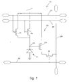
- a photo-sensitive element or pixel 10 consists of an inversely polarized diode 11, two transistors, respectively a first 21 of the P-channel type and a second 22, of the N-channel type, to polarize the photo-diode, and an amplification and reading circuit 20 comprising two transistors, respectively third 23 and fourth 24.
- the first 21 and the second 22 transistors are of the CMOS type.
- the first transistor 21 is of the P-channel type, it is able to represent an ideal key
- the second transistor 22 is of the N-channel type it is able to represent an active load.
- the number of N-channel type transistors may vary from 1 to 12 in order to increase by a corresponding value the logarithmic conversion gain of the current photo-generated by the polarized diode 11.
- the pixel 10 is of the type able to detect light of a wavelength between 400 and 1000 nm and an intensity which varies in an interval of at least 8 decades, between 10 -5 and 10 3 W/m 2 , and is able to constitute the single cell of a multiple cell matrix sensor made entirely with CMOS technology and hence able to be integrated in a chip.
- the diode 11 is made by a joint between an N-type insulated diffusion, medium doped, which can be achieved by means of Nwell, or strongly doped, achieved by means of an N+ diffusion, and the silicon substrate which is weak doped P.
- the interface area between the two parts of the diode is emptied of free loads and characterized by the presence of an internal electric field which can be increased by inversely polarizing the diode even from outside.
- a mass contact has been put in the structure, in the substrate and the N-type diffusion remains insulated or is connected to a positive tension according to the state of the two transistors 21 and 22 which are piloted externally through the signal lines 26 and 27.
- the substrate P which represents a common point for the N-channel transistors, weakly doped, is mass polarized.
- the P-channel transistor is made inside a deep diffusion achieved by means of a Nwell. The latter is polarized to a tension which, according to the embodiment, can be the feed tension or the tension of its source.
- the light In the emptied zone, the light generates electron-hole pairs which are separated from the electric field of the joint, giving origin to a current directly proportional to the incident light.
- the first P-channel transistor 21 is put in a conduction state by putting the signal 27 at a low tension (preferably mass); in this way the node 25 is polarized to the feed tension.
- the signal 27 is taken to a high tension so that the first transistor 21 enters an interdiction zone.
- the signal 26 is put at a fixed tension between a minimum and a maximum.
- the minimum value is represented by a tension equal to the threshold tension of the transistor; this guarantees that the so-called "blooming" effect is excluded.
- the maximum value is represented by the feed tension or, in extreme cases, by an external superfeed.
- the diode 11 occupies about 40% of the total surface of the pixel 10, and has a good conversion efficiency throughout the whole spectrum of the visible and nearby infra-red light.
- the pixel 10 has maximum sensitivity to radiation in the nearby infra-red, between about 800 and about 1000 nm, because this radiation is composed of photons of energy suitable to penetrate the silicon and reach the emptied area of the photo-diode and there generate pairs of electric loads.
- the amplification and reading circuit 20 substantially consists of a third transistor 23 and a fourth transistor 24, each of which has its own specific function.
- the transistor 23, made according to the known configuration called tension follower, or common drain or source follower, achieves the first stage of current amplification of the signal, transferring the tension present on the photo-sensitive node 25 to the drain of the fourth transistor 24, with a gain in tension near to one; enabling the fourth transistor 24 allows to connect the pixel 10 with an output line 28 (called bitline) with the advantage of transferring the tension of the photo-sensitive node 25 to the bitline without losses, something which would not be possible in the absence of the amplification transistor 23.
- tension follower or common drain or source follower
- the pixels 10 made in this way are organized in a two-dimensional matrix for the vision of complete scenes, but every sub-sampling of the matrix into subsets is possible.
- a second configuration of the pixel, not shown here, is possible.
- the polarity of the diode is inverted, all the N-channel transistors are replaced by P-channel transistors, the P-channel transistor is replaced by an N-channel transistor, while the positive feed terminals and the mass are inverted.
- This configuration has a very similar functioning to that of the configuration described above.
- the signal is detected at two different moments, it is performed in hardware mode, by means of subtraction of the two signals, the correction of the reading noise, both in linear and logarithmic mode.
- This correction is possible thanks to the presence of the P-channel transistor 21 which functions as an ideal key or switch and allows to eliminate the "settling down” error which occurs if only the N-channel transistor is used.
- the "settling down” error is due to the fact that the N-channel transistor uses a certain time before taking the pixel from the value immediately after transition, which depends on the value from which it starts, to the final reset tension; this time is typically more than the reset time. This causes a certain uncertainty on the value obtained after subtraction of the reset signal and the integration signal, and hence additional noise.
- the final reset value depends in any case in logarithmic mode on the light present.
- the pixel can be used as a purely logarithmic pixel; in this case, the current is continually transformed into tension and the signal can be read at any moment whatsoever, with a frequency of reading which can even reach 20 MHz, identifying any pixel 10 in the matrix.
- the pixel is used in its original configuration, it is also necessary to introduce an amplification stage on the level of the columns of the pixel matrix which makes a subtraction of the reset signal and the integration signal and a first amplification; this component is not shown in the drawing either.
- CMOS type technology can be used to make the sensor, that is, a process to make the microelectronic circuits in silicon, in order to obtain photo-sensitive elements with satisfactory electro-optical characteristics without having to develop a dedicated technology.
Landscapes
- Physics & Mathematics (AREA)
- Nonlinear Science (AREA)
- Engineering & Computer Science (AREA)
- Multimedia (AREA)
- Signal Processing (AREA)
- Solid State Image Pick-Up Elements (AREA)
- Liquid Crystal (AREA)
- Measurement Of Current Or Voltage (AREA)
- Transforming Light Signals Into Electric Signals (AREA)
- Photometry And Measurement Of Optical Pulse Characteristics (AREA)
Applications Claiming Priority (2)
| Application Number | Priority Date | Filing Date | Title |
|---|---|---|---|
| IT000226A ITUD20030226A1 (it) | 2003-11-17 | 2003-11-17 | Elemento fotosensibile per sensori elettro-ottici. |
| ITUD20030226 | 2003-11-17 |
Publications (3)
| Publication Number | Publication Date |
|---|---|
| EP1533995A2 true EP1533995A2 (de) | 2005-05-25 |
| EP1533995A3 EP1533995A3 (de) | 2005-06-08 |
| EP1533995B1 EP1533995B1 (de) | 2008-02-13 |
Family
ID=34430829
Family Applications (1)
| Application Number | Title | Priority Date | Filing Date |
|---|---|---|---|
| EP04105785A Expired - Lifetime EP1533995B1 (de) | 2003-11-17 | 2004-11-15 | Photoempfindliches Element für elektrooptische Sensoren |
Country Status (5)
| Country | Link |
|---|---|
| US (1) | US7119320B2 (de) |
| EP (1) | EP1533995B1 (de) |
| AT (1) | ATE386401T1 (de) |
| DE (1) | DE602004011731D1 (de) |
| IT (1) | ITUD20030226A1 (de) |
Families Citing this family (2)
| Publication number | Priority date | Publication date | Assignee | Title |
|---|---|---|---|---|
| TWI556644B (zh) | 2014-01-10 | 2016-11-01 | 恆景科技股份有限公司 | 像素電路和影像感測器 |
| CN108735182B (zh) * | 2018-05-04 | 2021-04-09 | 京东方科技集团股份有限公司 | 一种感光电路及其驱动方法、显示装置 |
Family Cites Families (7)
| Publication number | Priority date | Publication date | Assignee | Title |
|---|---|---|---|---|
| DE4209536C3 (de) * | 1992-03-24 | 2000-10-05 | Stuttgart Mikroelektronik | Bildzelle für einen Bildaufnehmer-Chip |
| US5917547A (en) * | 1997-07-21 | 1999-06-29 | Foveonics, Inc. | Two-stage amplifier for active pixel sensor cell array for reducing fixed pattern noise in the array output |
| USRE38499E1 (en) * | 1997-07-21 | 2004-04-20 | Foveon, Inc. | Two-stage amplifier for active pixel sensor cell array for reducing fixed pattern noise in the array output |
| US6323479B1 (en) * | 1998-09-16 | 2001-11-27 | Dalsa, Inc. | Sensor pixel with linear and logarithmic response |
| WO2000036821A1 (fr) | 1998-12-11 | 2000-06-22 | Yiming Zhu | Capteur d'images a acces aleatoire en technologie cmos a filtrage passe-bas integre |
| US6967682B1 (en) | 1999-03-29 | 2005-11-22 | Minolta Co., Ltd. | Photoelectric converting device |
| US6731397B1 (en) * | 1999-05-21 | 2004-05-04 | Foveon, Inc. | Method for storing and retrieving digital image data from an imaging array |
-
2003
- 2003-11-17 IT IT000226A patent/ITUD20030226A1/it unknown
-
2004
- 2004-03-19 US US10/804,136 patent/US7119320B2/en not_active Expired - Fee Related
- 2004-11-15 AT AT04105785T patent/ATE386401T1/de not_active IP Right Cessation
- 2004-11-15 EP EP04105785A patent/EP1533995B1/de not_active Expired - Lifetime
- 2004-11-15 DE DE602004011731T patent/DE602004011731D1/de not_active Expired - Lifetime
Also Published As
| Publication number | Publication date |
|---|---|
| US20050103982A1 (en) | 2005-05-19 |
| US7119320B2 (en) | 2006-10-10 |
| ITUD20030226A1 (it) | 2005-05-18 |
| DE602004011731D1 (de) | 2008-03-27 |
| ATE386401T1 (de) | 2008-03-15 |
| EP1533995B1 (de) | 2008-02-13 |
| EP1533995A3 (de) | 2005-06-08 |
Similar Documents
| Publication | Publication Date | Title |
|---|---|---|
| CN1833429B (zh) | 双转换增益成像器 | |
| US6140630A (en) | Vcc pump for CMOS imagers | |
| JP4331185B2 (ja) | 画素単位の飽和防止機能を有するイメージセンサ | |
| US8026969B2 (en) | Pixel for boosting pixel reset voltage | |
| US9591245B2 (en) | Image sensor pixels with adjustable body bias | |
| US9854194B2 (en) | CMOS active pixel structure | |
| KR101437912B1 (ko) | 이미지 센서의 구동 방법 | |
| US7586487B2 (en) | Solid state imaging apparatus and method for driving the same | |
| US7502060B2 (en) | Solid-state imaging device providing wide dynamic range and high low-illuminance sensitivity | |
| CN101796810A (zh) | 具有高功能动态性的cmos有源像素 | |
| US20080284890A1 (en) | Solid-state image-sensing device | |
| JP2003202264A (ja) | 光検出器、光電子イメージセンサ及び電磁放射を検出する方法 | |
| US6831691B1 (en) | Solid-state image pickup device | |
| US7015448B2 (en) | Dark current reduction circuitry for CMOS active pixel sensors | |
| US20120267695A1 (en) | Solid state imaging device | |
| US6891144B2 (en) | Photo-sensitive element for electro-optical sensors | |
| US9743027B2 (en) | Image sensor with high dynamic range and method | |
| US7119320B2 (en) | Photo-sensitive element for electro-optical sensors operating under various illumination conditions | |
| JP2001094878A (ja) | 固体撮像装置 | |
| KR101194873B1 (ko) | 넓은 다이나믹 레인지를 가지는 고감도 cmos 영상 센서 장치 | |
| KR20180011562A (ko) | 단위 픽셀 장치 및 그 동작 방법 | |
| CN115134541B (zh) | 一种同时具有高低增益和对数响应的高动态cmos图像传感器及时序控制方法和读取方式 | |
| JP2001103379A (ja) | 固体撮像装置 | |
| US7378638B2 (en) | Photo-sensitive element used in electro-optical sensors to detect and convert incident light into an electrical signal | |
| US20050103975A1 (en) | Imager |
Legal Events
| Date | Code | Title | Description |
|---|---|---|---|
| PUAI | Public reference made under article 153(3) epc to a published international application that has entered the european phase |
Free format text: ORIGINAL CODE: 0009012 |
|
| PUAL | Search report despatched |
Free format text: ORIGINAL CODE: 0009013 |
|
| AK | Designated contracting states |
Kind code of ref document: A2 Designated state(s): AT BE BG CH CY CZ DE DK EE ES FI FR GB GR HU IE IS IT LI LU MC NL PL PT RO SE SI SK TR |
|
| AX | Request for extension of the european patent |
Extension state: AL HR LT LV MK YU |
|
| AK | Designated contracting states |
Kind code of ref document: A3 Designated state(s): AT BE BG CH CY CZ DE DK EE ES FI FR GB GR HU IE IS IT LI LU MC NL PL PT RO SE SI SK TR |
|
| AX | Request for extension of the european patent |
Extension state: AL HR LT LV MK YU |
|
| 17P | Request for examination filed |
Effective date: 20051207 |
|
| AKX | Designation fees paid |
Designated state(s): AT BE BG CH CY CZ DE DK EE ES FI FR GB GR HU IE IS IT LI LU MC NL PL PT RO SE SI SK TR |
|
| GRAP | Despatch of communication of intention to grant a patent |
Free format text: ORIGINAL CODE: EPIDOSNIGR1 |
|
| RIN1 | Information on inventor provided before grant (corrected) |
Inventor name: VATTERONI, MONICA Inventor name: SARTORI, ALVISE |
|
| GRAS | Grant fee paid |
Free format text: ORIGINAL CODE: EPIDOSNIGR3 |
|
| GRAA | (expected) grant |
Free format text: ORIGINAL CODE: 0009210 |
|
| AK | Designated contracting states |
Kind code of ref document: B1 Designated state(s): AT BE BG CH CY CZ DE DK EE ES FI FR GB GR HU IE IS IT LI LU MC NL PL PT RO SE SI SK TR |
|
| REG | Reference to a national code |
Ref country code: GB Ref legal event code: FG4D |
|
| REG | Reference to a national code |
Ref country code: CH Ref legal event code: EP |
|
| RAP2 | Party data changed (patent owner data changed or rights of a patent transferred) |
Owner name: NEURICAM SPA |
|
| REG | Reference to a national code |
Ref country code: IE Ref legal event code: FG4D |
|
| REF | Corresponds to: |
Ref document number: 602004011731 Country of ref document: DE Date of ref document: 20080327 Kind code of ref document: P |
|
| NLT2 | Nl: modifications (of names), taken from the european patent patent bulletin |
Owner name: NEURICAM SPA Effective date: 20080319 |
|
| PG25 | Lapsed in a contracting state [announced via postgrant information from national office to epo] |
Ref country code: IS Free format text: LAPSE BECAUSE OF FAILURE TO SUBMIT A TRANSLATION OF THE DESCRIPTION OR TO PAY THE FEE WITHIN THE PRESCRIBED TIME-LIMIT Effective date: 20080613 Ref country code: FI Free format text: LAPSE BECAUSE OF FAILURE TO SUBMIT A TRANSLATION OF THE DESCRIPTION OR TO PAY THE FEE WITHIN THE PRESCRIBED TIME-LIMIT Effective date: 20080213 Ref country code: ES Free format text: LAPSE BECAUSE OF FAILURE TO SUBMIT A TRANSLATION OF THE DESCRIPTION OR TO PAY THE FEE WITHIN THE PRESCRIBED TIME-LIMIT Effective date: 20080524 |
|
| NLV1 | Nl: lapsed or annulled due to failure to fulfill the requirements of art. 29p and 29m of the patents act | ||
| PG25 | Lapsed in a contracting state [announced via postgrant information from national office to epo] |
Ref country code: AT Free format text: LAPSE BECAUSE OF FAILURE TO SUBMIT A TRANSLATION OF THE DESCRIPTION OR TO PAY THE FEE WITHIN THE PRESCRIBED TIME-LIMIT Effective date: 20080213 |
|
| PG25 | Lapsed in a contracting state [announced via postgrant information from national office to epo] |
Ref country code: BE Free format text: LAPSE BECAUSE OF FAILURE TO SUBMIT A TRANSLATION OF THE DESCRIPTION OR TO PAY THE FEE WITHIN THE PRESCRIBED TIME-LIMIT Effective date: 20080213 Ref country code: SI Free format text: LAPSE BECAUSE OF FAILURE TO SUBMIT A TRANSLATION OF THE DESCRIPTION OR TO PAY THE FEE WITHIN THE PRESCRIBED TIME-LIMIT Effective date: 20080213 Ref country code: PL Free format text: LAPSE BECAUSE OF FAILURE TO SUBMIT A TRANSLATION OF THE DESCRIPTION OR TO PAY THE FEE WITHIN THE PRESCRIBED TIME-LIMIT Effective date: 20080213 |
|
| PG25 | Lapsed in a contracting state [announced via postgrant information from national office to epo] |
Ref country code: SE Free format text: LAPSE BECAUSE OF FAILURE TO SUBMIT A TRANSLATION OF THE DESCRIPTION OR TO PAY THE FEE WITHIN THE PRESCRIBED TIME-LIMIT Effective date: 20080513 Ref country code: CZ Free format text: LAPSE BECAUSE OF FAILURE TO SUBMIT A TRANSLATION OF THE DESCRIPTION OR TO PAY THE FEE WITHIN THE PRESCRIBED TIME-LIMIT Effective date: 20080213 Ref country code: SK Free format text: LAPSE BECAUSE OF FAILURE TO SUBMIT A TRANSLATION OF THE DESCRIPTION OR TO PAY THE FEE WITHIN THE PRESCRIBED TIME-LIMIT Effective date: 20080213 Ref country code: PT Free format text: LAPSE BECAUSE OF FAILURE TO SUBMIT A TRANSLATION OF THE DESCRIPTION OR TO PAY THE FEE WITHIN THE PRESCRIBED TIME-LIMIT Effective date: 20080714 Ref country code: NL Free format text: LAPSE BECAUSE OF FAILURE TO SUBMIT A TRANSLATION OF THE DESCRIPTION OR TO PAY THE FEE WITHIN THE PRESCRIBED TIME-LIMIT Effective date: 20080213 Ref country code: DK Free format text: LAPSE BECAUSE OF FAILURE TO SUBMIT A TRANSLATION OF THE DESCRIPTION OR TO PAY THE FEE WITHIN THE PRESCRIBED TIME-LIMIT Effective date: 20080213 |
|
| PG25 | Lapsed in a contracting state [announced via postgrant information from national office to epo] |
Ref country code: RO Free format text: LAPSE BECAUSE OF FAILURE TO SUBMIT A TRANSLATION OF THE DESCRIPTION OR TO PAY THE FEE WITHIN THE PRESCRIBED TIME-LIMIT Effective date: 20080213 |
|
| EN | Fr: translation not filed | ||
| PLBE | No opposition filed within time limit |
Free format text: ORIGINAL CODE: 0009261 |
|
| STAA | Information on the status of an ep patent application or granted ep patent |
Free format text: STATUS: NO OPPOSITION FILED WITHIN TIME LIMIT |
|
| 26N | No opposition filed |
Effective date: 20081114 |
|
| PG25 | Lapsed in a contracting state [announced via postgrant information from national office to epo] |
Ref country code: DE Free format text: LAPSE BECAUSE OF FAILURE TO SUBMIT A TRANSLATION OF THE DESCRIPTION OR TO PAY THE FEE WITHIN THE PRESCRIBED TIME-LIMIT Effective date: 20080514 |
|
| PG25 | Lapsed in a contracting state [announced via postgrant information from national office to epo] |
Ref country code: FR Free format text: LAPSE BECAUSE OF FAILURE TO SUBMIT A TRANSLATION OF THE DESCRIPTION OR TO PAY THE FEE WITHIN THE PRESCRIBED TIME-LIMIT Effective date: 20081205 Ref country code: BG Free format text: LAPSE BECAUSE OF FAILURE TO SUBMIT A TRANSLATION OF THE DESCRIPTION OR TO PAY THE FEE WITHIN THE PRESCRIBED TIME-LIMIT Effective date: 20080513 Ref country code: EE Free format text: LAPSE BECAUSE OF FAILURE TO SUBMIT A TRANSLATION OF THE DESCRIPTION OR TO PAY THE FEE WITHIN THE PRESCRIBED TIME-LIMIT Effective date: 20080213 |
|
| PG25 | Lapsed in a contracting state [announced via postgrant information from national office to epo] |
Ref country code: MC Free format text: LAPSE BECAUSE OF NON-PAYMENT OF DUE FEES Effective date: 20081130 |
|
| REG | Reference to a national code |
Ref country code: CH Ref legal event code: PL |
|
| GBPC | Gb: european patent ceased through non-payment of renewal fee |
Effective date: 20081115 |
|
| PG25 | Lapsed in a contracting state [announced via postgrant information from national office to epo] |
Ref country code: CY Free format text: LAPSE BECAUSE OF FAILURE TO SUBMIT A TRANSLATION OF THE DESCRIPTION OR TO PAY THE FEE WITHIN THE PRESCRIBED TIME-LIMIT Effective date: 20080213 |
|
| PG25 | Lapsed in a contracting state [announced via postgrant information from national office to epo] |
Ref country code: CH Free format text: LAPSE BECAUSE OF NON-PAYMENT OF DUE FEES Effective date: 20081130 Ref country code: IE Free format text: LAPSE BECAUSE OF NON-PAYMENT OF DUE FEES Effective date: 20081117 Ref country code: LI Free format text: LAPSE BECAUSE OF NON-PAYMENT OF DUE FEES Effective date: 20081130 |
|
| PG25 | Lapsed in a contracting state [announced via postgrant information from national office to epo] |
Ref country code: GB Free format text: LAPSE BECAUSE OF NON-PAYMENT OF DUE FEES Effective date: 20081115 |
|
| PG25 | Lapsed in a contracting state [announced via postgrant information from national office to epo] |
Ref country code: HU Free format text: LAPSE BECAUSE OF FAILURE TO SUBMIT A TRANSLATION OF THE DESCRIPTION OR TO PAY THE FEE WITHIN THE PRESCRIBED TIME-LIMIT Effective date: 20080814 Ref country code: LU Free format text: LAPSE BECAUSE OF NON-PAYMENT OF DUE FEES Effective date: 20081115 |
|
| PG25 | Lapsed in a contracting state [announced via postgrant information from national office to epo] |
Ref country code: TR Free format text: LAPSE BECAUSE OF FAILURE TO SUBMIT A TRANSLATION OF THE DESCRIPTION OR TO PAY THE FEE WITHIN THE PRESCRIBED TIME-LIMIT Effective date: 20080213 |
|
| PG25 | Lapsed in a contracting state [announced via postgrant information from national office to epo] |
Ref country code: GR Free format text: LAPSE BECAUSE OF FAILURE TO SUBMIT A TRANSLATION OF THE DESCRIPTION OR TO PAY THE FEE WITHIN THE PRESCRIBED TIME-LIMIT Effective date: 20080514 |
|
| P01 | Opt-out of the competence of the unified patent court (upc) registered |
Effective date: 20230520 |
|
| PGFP | Annual fee paid to national office [announced via postgrant information from national office to epo] |
Ref country code: IT Payment date: 20231107 Year of fee payment: 20 |