EP1533905A2 - Imprint-free coding for ferroelectric nonvolatile counters - Google Patents
Imprint-free coding for ferroelectric nonvolatile counters Download PDFInfo
- Publication number
- EP1533905A2 EP1533905A2 EP04254400A EP04254400A EP1533905A2 EP 1533905 A2 EP1533905 A2 EP 1533905A2 EP 04254400 A EP04254400 A EP 04254400A EP 04254400 A EP04254400 A EP 04254400A EP 1533905 A2 EP1533905 A2 EP 1533905A2
- Authority
- EP
- European Patent Office
- Prior art keywords
- encoder
- input
- signal
- output
- equal
- Prior art date
- Legal status (The legal status is an assumption and is not a legal conclusion. Google has not performed a legal analysis and makes no representation as to the accuracy of the status listed.)
- Withdrawn
Links
Images


Classifications
-
- G—PHYSICS
- G11—INFORMATION STORAGE
- G11C—STATIC STORES
- G11C11/00—Digital stores characterised by the use of particular electric or magnetic storage elements; Storage elements therefor
- G11C11/21—Digital stores characterised by the use of particular electric or magnetic storage elements; Storage elements therefor using electric elements
- G11C11/22—Digital stores characterised by the use of particular electric or magnetic storage elements; Storage elements therefor using electric elements using ferroelectric elements
-
- H—ELECTRICITY
- H03—ELECTRONIC CIRCUITRY
- H03K—PULSE TECHNIQUE
- H03K23/00—Pulse counters comprising counting chains; Frequency dividers comprising counting chains
- H03K23/76—Pulse counters comprising counting chains; Frequency dividers comprising counting chains using magnetic cores or ferro-electric capacitors
Definitions
- the present invention relates to coding methods, and more particularly, to a coding method that substantially reduces imprint when used in conjunction with ferroelectric nonvolatile counters.
- Ferroelectric materials such as lead-zirconate-titanate (“PZT”) can be used as the dielectric material in a ferroelectric capacitor that in turn is used as the memory element in a nonvolatile memory cell, latch, or counter.
- PZT lead-zirconate-titanate
- a ferroelectric capacitor In order to be useful as the memory element in a semiconductor nonvolatile memory, latch, or counter, however, a ferroelectric capacitor must retain data for an extended period of time at a given storage temperature. The ability to retain data, also known as retention performance, is adversely affected by a multifaceted mechanism known generally by those skilled in the art as "imprint”. The term imprint is used because it implies that the history of the data stored in the ferroelectric capacitor affects its present retention performance. Specifically, storage or writing of data of the same binary value for a long period of time at temperature undesirably degrades the ability of the ferroelectric capacitor to retain data of the opposite binary value.
- a ferroelectric nonvolatile counter In a ferroelectric nonvolatile counter, the most significant bits stay at a logic zero data state until the count number is large enough to flip the logic state to a logic one data state, if conventional binary coding methods are used. For a counter with a large number of bits, the most significant bits are written (clocked) to the logic zero data state many times before they are eventually written to a logic one data state. For example, in a 40 bit counter, the most significant bit is written to a logic zero data state 2 39 times, which is about 10 12 times, before it is finally written to a logic one data state. Thus, this most significant bit and the associated nonvolatile ferroelectric capacitor is very significantly imprinted to the logic zero data state, and the imprinting will therefore negatively impact its ability to retain the logic one data state.
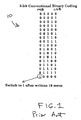
- FIG. 1 a prior art conventional five-bit binary coding scheme is shown. Note that while the least-significant bit (“LSB”) switches with every advancement of the count, the most-significant bit (“MSB”) does not switch until sixteen zero data states have been written to the associated ferroelectric capacitor. Of course, the imprint problem increases for the most-significant bits as the total number of bits in the counter increases.
- LSB least-significant bit
- MSB most-significant bit
- a coding method suitable for use with ferroelectric or other nonvolatile counters subject to imprint ensures that all of the bits in the code are frequently switched and not left in a fixed data state.
- the general coding equation for this method is such that: for an even integer n, the output code is represented by the conventional binary code of n/2; for an odd integer n, the output code is represented by the conventional binary code of the one's compliment of (n - 1)/2.
- every bit switches to its compliment when counting from an even number to an odd number. Since every bit switches at least once every two counts, imprint is substantially reduced.
- the maximal number is encoded to 1000, instead of 1111, in a four-bit coding scheme.
- a digital encoder including a XNOR gate, a "plus one” operation logic block, and a two-to-one multiplexer for converting an inverted input signal into an encoded output signal.
- the digital encoder also includes "up/down” and most-significant bit inputs.
- equation (1) The general equation for the coding method of the present invention is given by equation (1):
- the encoded output is represented by the conventional binary code of n /2; for an odd integer n , the encoded output is represented by the conventional binary code of the one's compliment of ( n - 1)/2.
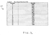
- a four-bit counter for example, we have the encoding output 20 shown in FIG. 2 (Table I). Every bit switches to its compliment when counting from an even number to an odd number. Thus, imprint is substantially reduced.
- the maximal number is encoded to 1000, instead of 1111, in the case of a four-bit counter.
- Applying this method to a five-bit counter for example, we have the encoding output 22 shown in FIG. 3 (Table II). Every bit switches to its compliment when counting from an even number to an odd number. Thus, imprint is substantially reduced.
- the maximal number is encoded to 10000, instead of 11111, in the case of a five-bit counter.
- the output is kept at zero when counting down from zero, instead of rolling over to the maximal number.
- the output is kept at the maximal number when counting up from the maximal number, instead of rolling over to zero.
- FIG. 4 a digital logic circuitry implementation of an encoder 30 is shown using the coding method of the present invention.
- the bold lines in FIG. 4 represents a bus having a width of m bits.
- Pin U/D on node 38 is set to a logic one for counting up and a logic zero for counting down.
- the signal on node 40, d ⁇ m > is the most significant bit of the input number.
- the output dout ⁇ m :0> is the result of counting up or counting down from d ⁇ m :0>.
- the signal on node 42, d ⁇ m :0> is an inverted input signal or the one's compliment of d ⁇ m :0>.
- Encoder 30 includes a "plus-one" operation block 34, which can be implemented using digital combinatorial circuitry as is known by those skilled in the art.
- the input of block 34 receives the inverted digital input signal d ⁇ m :0>, and the output of block 34 provides the output signal equal to d ⁇ m :0> + 1.
- a first input of the two-to-one multiplexer 36 receives the inverted input signal d ⁇ m:0>, and a second input receives the output signal d ⁇ m :0> + 1 on output node 46.
- a XNOR gate 32 has a first input for receiving an up-down ("U/D") signal on node 38, a second input for receiving a most-significant bit input signal ("d ⁇ m >") on node 40, and an output 48 for providing a control signal to multiplexer 36.
- the output signal dout ⁇ m :0> of the encoder 30 is provided at multiplexer output node 50.
- the output signal is equal to d if the control signal on node 48 is a logic zero, and is equal to d + 1 if the control signal on node 48 is a logic one.
- the output signal on node 50 can be input to m ferroelectric latches in parallel in an m -bit counter, corresponding to the width of the m -bit bus.
- m ferroelectric latches in parallel in an m -bit counter, corresponding to the width of the m -bit bus.
- a counter having four or five ferroelectric latches corresponding to the coding schemes shown in FIGS. 2 and 3 can be used.
- the complemented output of the latches can be fed back to node 42 to complete a ferroelectric counter including encoder 30.
- Other implementations of a full m -bit ferroelectric counter are also possible in which imprint effects can be minimized.
Landscapes
- Engineering & Computer Science (AREA)
- Computer Hardware Design (AREA)
- Power Engineering (AREA)
- Compression, Expansion, Code Conversion, And Decoders (AREA)
Abstract
Description

| Counting up from n = dmdm -1 dm -2...d 1 d 0 | ||
| n | n + 1 | |
| n is even, i.e. dm is 0 | ⇒ | n+1= |
| n is odd, i.e. dm is 1 | ⇒ | n + 1 = |
| Counting down from n=dmdm -1 dm -2...d 1 d 0 | ||
| n | n - 1 | |
| n is even, i.e. dm is 0 | ⇒ | n-1= |
| n is odd, i.e. dm is 1 | ⇒ | n - 1= |
Claims (20)
- An encoder for use in a nonvolatile counter comprising:a logic gate having a first input for receiving an up/down signal, a second input for receiving a most-significant bit signal;a plus-one block having an input for receiving an inverted input signal and an output; anda two-to-one multiplexer having a first input for receiving the inverted input signal, a second input coupled to the output of the plus-one block, a control input coupled to the output of the logic gate, and an output for providing an encoded signal.
- The encoder of claim 1 in which the first input is set to a logic one for counting up.
- The encoder of claim 1 in which the first input is set to a logic zero for counting down.
- The encoder of claim 1 in which the logic gate comprises a XNOR gate.
- The encoder of claim 1 in which the plus-one block comprises a combinatorial logic circuit.
- The encoder of claim 1 in which the encoded signal is equal to the inverted input signal if the control signal is a logic zero.
- The encoder of claim 1 in which the encoded signal is equal to the inverted input signal plus one if the control signal is a logic one.
- The encoder of claim 1 in which the nonvolatile counter comprises a ferroelectric nonvolatile counter.
- The encoder of claim 1 in which the nonvolatile counter comprises an m-bit nonvolatile counter.
- The encoder of claim 9 in which m is equal to 4.
- The encoder of claim 9 in which m is equal to 5.
- The encoder of claim 9 in which m is equal to 40.
- A method for encoding an input number n comprising:if n is even, providing a conventional binary code of (n/2); andif n is odd, providing a complementary binary code of ((n-1)/2).
- A method for encoding an input signal to an output signal comprising switching all of the bits in the output signal to the logical compliment when counting from an even number to an odd number.
- A method for counting up from an input number n = dmdm -1 dm -2...d 1 d 0 comprising:if n is even, then n+1=
d md m -1d m -2...d 1d 0; andif n is odd, then n + 1 =d md m -1d m -z...d 1d 0 + 1. - The method of claim 15 further comprising keeping an output count at a maximal number when counting up from the maximal number instead of rolling the output count over to zero.
- The method of claim 16 in which the maximal number is equal to 1000 when m is equal to four.
- A method for counting down from an input number n = dmdm -1 dm -2...d 1 d 0 comprising:if n is even, then n - 1=
d md m -1d m -2...d 1d 0 +1; andif n is odd, then n - 1 =d md m -1d m -2 ...d 1 d 0. - The method of claim 18 further comprising keeping an output count at zero when counting down from zero, instead of rolling the output count over to a maximal number.
- The method of claim 18 in which the maximal number is equal to 1000 when m is equal to four.
Applications Claiming Priority (2)
| Application Number | Priority Date | Filing Date | Title |
|---|---|---|---|
| US719108 | 1985-04-02 | ||
| US10/719,108 US7176824B2 (en) | 2003-11-21 | 2003-11-21 | Imprint-free coding for ferroelectric nonvolatile counters |
Publications (2)
| Publication Number | Publication Date |
|---|---|
| EP1533905A2 true EP1533905A2 (en) | 2005-05-25 |
| EP1533905A3 EP1533905A3 (en) | 2006-11-22 |
Family
ID=34435799
Family Applications (1)
| Application Number | Title | Priority Date | Filing Date |
|---|---|---|---|
| EP04254400A Withdrawn EP1533905A3 (en) | 2003-11-21 | 2004-07-23 | Imprint-free coding for ferroelectric nonvolatile counters |
Country Status (2)
| Country | Link |
|---|---|
| US (2) | US7176824B2 (en) |
| EP (1) | EP1533905A3 (en) |
Families Citing this family (6)
| Publication number | Priority date | Publication date | Assignee | Title |
|---|---|---|---|---|
| US20080168215A1 (en) * | 2007-01-05 | 2008-07-10 | Anxiao Jiang | Storing Information in a Memory |
| WO2008086233A1 (en) * | 2007-01-05 | 2008-07-17 | The Texas A & M University System, A Texas State Agency | Storing information in a memory |
| US7573969B2 (en) * | 2007-09-27 | 2009-08-11 | Sandisk Il Ltd. | Counter using shift for enhanced endurance |
| US8081500B2 (en) * | 2009-03-31 | 2011-12-20 | Ramtron International Corporation | Method for mitigating imprint in a ferroelectric memory |
| JP2017028409A (en) * | 2015-07-17 | 2017-02-02 | 富士通セミコンダクター株式会社 | Nonvolatile counter circuit, memory control method, and program |
| US10475524B2 (en) | 2016-09-15 | 2019-11-12 | Apple Inc. | Recovery of data read from memory with unknown polarity |
Family Cites Families (11)
| Publication number | Priority date | Publication date | Assignee | Title |
|---|---|---|---|---|
| US3651415A (en) * | 1970-12-21 | 1972-03-21 | Teletype Corp | Bidirectional counter |
| JP3355595B2 (en) * | 1996-03-25 | 2002-12-09 | シャープ株式会社 | Nonvolatile semiconductor memory device |
| US5912846A (en) * | 1997-02-28 | 1999-06-15 | Ramtron International Corporation | Serial ferroelectric random access memory architecture to equalize column accesses and improve data retention reliability by mitigating imprint effects |
| US5745403A (en) * | 1997-02-28 | 1998-04-28 | Ramtron International Corporation | System and method for mitigating imprint effect in ferroelectric random access memories utilizing a complementary data path |
| JP3003631B2 (en) * | 1997-06-23 | 2000-01-31 | 日本電気株式会社 | Nonvolatile semiconductor memory device |
| JP3770717B2 (en) * | 1997-11-26 | 2006-04-26 | ローム株式会社 | Ferroelectric memory device and method for correcting adhesion of ferroelectric memory element |
| JP2001093286A (en) | 1999-09-21 | 2001-04-06 | Nec Corp | Ferroelectric storage device and its manufacturing method |
| US6246603B1 (en) * | 2000-06-30 | 2001-06-12 | Stmicroelectronics, Inc. | Circuit and method for substantially preventing imprint effects in a ferroelectric memory device |
| JP2002184172A (en) * | 2000-10-04 | 2002-06-28 | Rohm Co Ltd | Data storage device |
| US6590798B1 (en) * | 2002-05-08 | 2003-07-08 | Texas Instruments Incorporated | Apparatus and methods for imprint reduction for ferroelectric memory cell |
| US6794997B2 (en) * | 2003-02-18 | 2004-09-21 | Sun Microsystems, Inc. | Extending non-volatile memory endurance using data encoding |
-
2003
- 2003-11-21 US US10/719,108 patent/US7176824B2/en not_active Expired - Lifetime
-
2004
- 2004-07-23 EP EP04254400A patent/EP1533905A3/en not_active Withdrawn
-
2006
- 2006-12-14 US US11/611,053 patent/US7271744B2/en not_active Expired - Lifetime
Also Published As
| Publication number | Publication date |
|---|---|
| US7176824B2 (en) | 2007-02-13 |
| EP1533905A3 (en) | 2006-11-22 |
| US7271744B2 (en) | 2007-09-18 |
| US20070085713A1 (en) | 2007-04-19 |
| US20050111287A1 (en) | 2005-05-26 |
Similar Documents
| Publication | Publication Date | Title |
|---|---|---|
| KR0142277B1 (en) | Memory system | |
| KR950008443B1 (en) | Memory containing 2- / N-valent conversion units | |
| US8732560B2 (en) | Method and device for correction of ternary stored binary data | |
| EP0646932B1 (en) | Circuit for decoding variable-length code, and system for decoding variable-length code which uses the circuit | |
| EP1410509B1 (en) | Non-power-of-two gray-code counter system having binary incrementer with counts distributed with bilateral symmetry | |
| US11430491B2 (en) | Device and method for reading data in memory | |
| JP2005100527A (en) | Semiconductor nonvolatile memory device | |
| EP0467678B1 (en) | Variable length coding apparatus and variable length decoding apparatus | |
| US7369441B2 (en) | Sensing circuit for multi-level flash memory | |
| EP1533905A2 (en) | Imprint-free coding for ferroelectric nonvolatile counters | |
| CN110619906A (en) | Readout circuit and readout method of multilevel phase change memory | |
| US5404138A (en) | Apparatus for decoding variable length codes | |
| US20050270043A1 (en) | Digital potentiometer with resistor binary weighting decoding | |
| US5048023A (en) | Asymmetric soft-error resistant memory | |
| WO1994019760A1 (en) | Semiconductor device | |
| US20220366948A1 (en) | Device and method for reading data in memory | |
| US6836525B1 (en) | Method for establishing a gray code and related counter circuit | |
| US7206876B2 (en) | Input/output interface of an integrated circuit device | |
| EP3889791B1 (en) | Efficient encoding methods | |
| US6360347B1 (en) | Error correction method for a memory device | |
| JP3784896B2 (en) | Viterbi decoder logic block | |
| CN117010032B (en) | SRAM physical unclonable function circuit capable of automatically reading and clearing and equipment | |
| EP0085762A2 (en) | Logic parity circuit | |
| JPH0440700A (en) | counter circuit | |
| Gregori et al. | An error control code scheme for multilevel Flash memories |
Legal Events
| Date | Code | Title | Description |
|---|---|---|---|
| PUAI | Public reference made under article 153(3) epc to a published international application that has entered the european phase |
Free format text: ORIGINAL CODE: 0009012 |
|
| AK | Designated contracting states |
Kind code of ref document: A2 Designated state(s): AT BE BG CH CY CZ DE DK EE ES FI FR GB GR HU IE IT LI LU MC NL PL PT RO SE SI SK TR |
|
| AX | Request for extension of the european patent |
Extension state: AL HR LT LV MK |
|
| PUAL | Search report despatched |
Free format text: ORIGINAL CODE: 0009013 |
|
| AK | Designated contracting states |
Kind code of ref document: A3 Designated state(s): AT BE BG CH CY CZ DE DK EE ES FI FR GB GR HU IE IT LI LU MC NL PL PT RO SE SI SK TR |
|
| AX | Request for extension of the european patent |
Extension state: AL HR LT LV MK |
|
| AKX | Designation fees paid | ||
| REG | Reference to a national code |
Ref country code: DE Ref legal event code: 8566 |
|
| STAA | Information on the status of an ep patent application or granted ep patent |
Free format text: STATUS: THE APPLICATION IS DEEMED TO BE WITHDRAWN |
|
| 18D | Application deemed to be withdrawn |
Effective date: 20070523 |