EP1531658A1 - Double sided wired circuit board - Google Patents
Double sided wired circuit board Download PDFInfo
- Publication number
- EP1531658A1 EP1531658A1 EP04025925A EP04025925A EP1531658A1 EP 1531658 A1 EP1531658 A1 EP 1531658A1 EP 04025925 A EP04025925 A EP 04025925A EP 04025925 A EP04025925 A EP 04025925A EP 1531658 A1 EP1531658 A1 EP 1531658A1
- Authority
- EP
- European Patent Office
- Prior art keywords
- insulating layer
- hole
- circuit board
- double sided
- conductor layers
- Prior art date
- Legal status (The legal status is an assumption and is not a legal conclusion. Google has not performed a legal analysis and makes no representation as to the accuracy of the status listed.)
- Withdrawn
Links
Images


Classifications
-
- H—ELECTRICITY
- H05—ELECTRIC TECHNIQUES NOT OTHERWISE PROVIDED FOR
- H05K—PRINTED CIRCUITS; CASINGS OR CONSTRUCTIONAL DETAILS OF ELECTRIC APPARATUS; MANUFACTURE OF ASSEMBLAGES OF ELECTRICAL COMPONENTS
- H05K3/00—Apparatus or processes for manufacturing printed circuits
- H05K3/40—Forming printed elements for providing electric connections to or between printed circuits
- H05K3/42—Plated through-holes or plated via connections
-
- H—ELECTRICITY
- H05—ELECTRIC TECHNIQUES NOT OTHERWISE PROVIDED FOR
- H05K—PRINTED CIRCUITS; CASINGS OR CONSTRUCTIONAL DETAILS OF ELECTRIC APPARATUS; MANUFACTURE OF ASSEMBLAGES OF ELECTRICAL COMPONENTS
- H05K3/00—Apparatus or processes for manufacturing printed circuits
- H05K3/40—Forming printed elements for providing electric connections to or between printed circuits
- H05K3/42—Plated through-holes or plated via connections
- H05K3/425—Plated through-holes or plated via connections characterised by the sequence of steps for plating the through-holes or via connections in relation to the conductive pattern
- H05K3/426—Plated through-holes or plated via connections characterised by the sequence of steps for plating the through-holes or via connections in relation to the conductive pattern initial plating of through-holes in substrates without metal
-
- H—ELECTRICITY
- H05—ELECTRIC TECHNIQUES NOT OTHERWISE PROVIDED FOR
- H05K—PRINTED CIRCUITS; CASINGS OR CONSTRUCTIONAL DETAILS OF ELECTRIC APPARATUS; MANUFACTURE OF ASSEMBLAGES OF ELECTRICAL COMPONENTS
- H05K3/00—Apparatus or processes for manufacturing printed circuits
- H05K3/40—Forming printed elements for providing electric connections to or between printed circuits
- H05K3/42—Plated through-holes or plated via connections
- H05K3/423—Plated through-holes or plated via connections characterised by electroplating method
-
- H—ELECTRICITY
- H05—ELECTRIC TECHNIQUES NOT OTHERWISE PROVIDED FOR
- H05K—PRINTED CIRCUITS; CASINGS OR CONSTRUCTIONAL DETAILS OF ELECTRIC APPARATUS; MANUFACTURE OF ASSEMBLAGES OF ELECTRICAL COMPONENTS
- H05K1/00—Printed circuits
- H05K1/02—Details
- H05K1/03—Use of materials for the substrate
- H05K1/0313—Organic insulating material
- H05K1/032—Organic insulating material consisting of one material
- H05K1/0346—Organic insulating material consisting of one material containing N
-
- H—ELECTRICITY
- H05—ELECTRIC TECHNIQUES NOT OTHERWISE PROVIDED FOR
- H05K—PRINTED CIRCUITS; CASINGS OR CONSTRUCTIONAL DETAILS OF ELECTRIC APPARATUS; MANUFACTURE OF ASSEMBLAGES OF ELECTRICAL COMPONENTS
- H05K1/00—Printed circuits
- H05K1/02—Details
- H05K1/11—Printed elements for providing electric connections to or between printed circuits
- H05K1/111—Pads for surface mounting, e.g. lay-out
- H05K1/112—Pads for surface mounting, e.g. lay-out directly combined with via connections
- H05K1/113—Via provided in pad; Pad over filled via
-
- H—ELECTRICITY
- H05—ELECTRIC TECHNIQUES NOT OTHERWISE PROVIDED FOR
- H05K—PRINTED CIRCUITS; CASINGS OR CONSTRUCTIONAL DETAILS OF ELECTRIC APPARATUS; MANUFACTURE OF ASSEMBLAGES OF ELECTRICAL COMPONENTS
- H05K2201/00—Indexing scheme relating to printed circuits covered by H05K1/00
- H05K2201/01—Dielectrics
- H05K2201/0137—Materials
- H05K2201/0154—Polyimide
-
- H—ELECTRICITY
- H05—ELECTRIC TECHNIQUES NOT OTHERWISE PROVIDED FOR
- H05K—PRINTED CIRCUITS; CASINGS OR CONSTRUCTIONAL DETAILS OF ELECTRIC APPARATUS; MANUFACTURE OF ASSEMBLAGES OF ELECTRICAL COMPONENTS
- H05K2201/00—Indexing scheme relating to printed circuits covered by H05K1/00
- H05K2201/09—Shape and layout
- H05K2201/09209—Shape and layout details of conductors
- H05K2201/095—Conductive through-holes or vias
- H05K2201/09563—Metal filled via
-
- H—ELECTRICITY
- H05—ELECTRIC TECHNIQUES NOT OTHERWISE PROVIDED FOR
- H05K—PRINTED CIRCUITS; CASINGS OR CONSTRUCTIONAL DETAILS OF ELECTRIC APPARATUS; MANUFACTURE OF ASSEMBLAGES OF ELECTRICAL COMPONENTS
- H05K3/00—Apparatus or processes for manufacturing printed circuits
- H05K3/10—Apparatus or processes for manufacturing printed circuits in which conductive material is applied to the insulating support in such a manner as to form the desired conductive pattern
- H05K3/108—Apparatus or processes for manufacturing printed circuits in which conductive material is applied to the insulating support in such a manner as to form the desired conductive pattern by semi-additive methods; masks therefor
-
- H—ELECTRICITY
- H05—ELECTRIC TECHNIQUES NOT OTHERWISE PROVIDED FOR
- H05K—PRINTED CIRCUITS; CASINGS OR CONSTRUCTIONAL DETAILS OF ELECTRIC APPARATUS; MANUFACTURE OF ASSEMBLAGES OF ELECTRICAL COMPONENTS
- H05K3/00—Apparatus or processes for manufacturing printed circuits
- H05K3/38—Improvement of the adhesion between the insulating substrate and the metal
- H05K3/388—Improvement of the adhesion between the insulating substrate and the metal by the use of a metallic or inorganic thin film adhesion layer
Definitions
- the present invention relates to a double sided wired circuit board and, more particularly, to a double sided wired circuit board with conductor layers formed on both sides of an insulating layer.
- the double sided flexible wired circuit board is a wired circuit board having wiring circuit patterns of a copper foil and the like formed on both sides of an insulating substrate of polyimide resin and the like.
- a through hole is formed in the insulating substrate to provide electrical conduction between the wired circuit patterns and a through hole plating is formed on an inside surface of the through hole.
- JP Laid-open (Unexamined) Patent Publication No. Hei 5-136562 proposes an elongate flexible board wherein metal foils used to form conductor circuits are integrally formed on both sides of the insulating substrate, and the conductor circuits formed on the both sides of the insulating substrate are electrically connected via the through hole.
- the through hole is plated in the ring-like form to extend along the inner circumference by the through hole plating, such that the through hole is hollow at a center thereof and is not filled with the plating material. Due to this, it is hard to form the wiring circuit pattern over the through hole and mount the electronic component thereon.
- the present invention provides a double sided wired circuit board comprising an insulating layer, and conductor layers formed on both sides of the insulating layer, wherein a through hole extending in a thickness direction of the insulating layer is formed in the insulating layer, and wherein the through hole is filled with a metal.
- the metal is formed by electrolytic plating.
- an end of the metal filled in the through hole can serve as a component mounting portion.
- the end of the metal can be used as a component mounting portion, and as such can allow the forming of the wiring circuit pattern on the component mounting portion or the mounting of electronic component thereon. This can provide enhancement of the high-density forming of the wiring circuit pattern and high-density mounting of the electronic component.
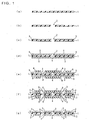
- FIG. 1 Shown in FIG. 1 is a production process drawing of a double sided flexible wired circuit board as a first embodiment of a double sided wired circuit board of the present invention. Referring to FIG. 1, the production method of the first embodiment of the double sided flexible wired circuit board will be described, first.
- an insulating layer 1 is prepared, first, as shown in FIG. 1(a).
- Any material may be used for the insulating layer 1 without any particular limitation, as long as it can be used for the insulating layer of a flexible wired circuit board.
- a synthetic resin film can be used as the insulating layer 1.
- the synthetic resin films that may be used include, for example, a polyimide resin film, polyamideimide resin film, an acrylic resin film, a polyether nitrile resin film, a polyether sulfonic resin film, a polyethylene terephthalate resin film, a polyethylene naphthalate resin film, and a polyvinyl chloride resin film.
- the polyimide resin film is used as the first insulating layer 1.
- the first insulating layer 1 has a thickness of e.g. 5-500 ⁇ m, or preferably 10-50 ⁇ m.
- a through hole 2 extending through the insulating layer 1 in a thickness direction thereof is formed in the insulating layer 1, as shown in FIG. 1(b).
- the through hole 2 can be formed by a known method, including machining such as drilling and punching, laser processing such as a YAG laser or an excimer laser, and a chemical etching.
- the through hole 2 may be formed simultaneously with the formation of the insulating layer 1 by using photosensitive synthetic resin for the insulating layer 1 and exposing it to light and developing it.
- the size and shape of the through hole 2 is properly selected for the intended purposes and applications.
- the through hole 2 is formed to have a maximum diameter of 20-300 ⁇ m, or preferably 30-150 ⁇ m, in terms of enhancement of high-density forming of the wiring circuit pattern and high-density mounting of the electronic component.
- the through hole 2 may be formed to extend along a direction perpendicular to a longitudinal direction of the insulating layer 1 (in a rectangular form in section as viewed from side) by machining and the like, as shown in FIG. 3(a).
- it may be formed in a tapered form that it becomes narrower gradually (or becomes wider gradually, though not shown) from one side of the insulating layer 1 to the other side of the same (a trapezoidal form in section as viewed from side) by laser processing or by a chemical etching and the like, as shown in FIG.
- 3(b) may be formed to obliquely extend with respect to the longitudinal direction of the insulating layer 1 and the direction perpendicular to the longitudinal direction of the same (a parallelogram form in section as viewed from side) by laser processing or by a chemical etching, as shown in FIG. 3(c).
- An angle ⁇ of obliquity of the through hole 2 with respect to a reference line L extending along the longitudinal direction of the insulating layer 1 shown in FIG. 3(b) and FIG. 3(c) (along a direction along which a front or back side of the insulating layer 1 extends) is preferably in the range of 40-70°.
- the through hole 2 is formed to extend along the perpendicular direction to the longitudinal direction of the insulating layer 1), so that the inside surface thereof extends vertically with respect to the longitudinal direction of the same, as shown in FIG. 3(a), there may be cases where it becomes hard to form the thin metal film 5 mentioned later by sputtering. Accordingly, it is preferable that the through hole 2 is formed in a tapered form shown in FIG. 3(b) or in an obliquely extending form shown in FIG. 3(c). In the case where the through hole 2 is formed obliquely, as shown in FIG. 3(c), thin metal films 5 are formed on both sides of the insulating layer 1 by sputtering from the both sides of the insulating layer 1.
- the conductor layers 3 are formed in the form of the wiring circuit pattern on both sides of the insulating layer 1 by the subtractive process, as shown in FIG. 1(c) to FIG. 1(g).
- the conductor portion 4 for providing electrical conduction between the conductor layers 3 is formed in the through hole 2 by filling conductive material in the through hole 2 with no substantial space therein.
- the thin metal films 5 serving as a seed film are formed on the both sides of the insulating layer 1 and around the inside surface of the through hole 2, first, as shown in FIG. 1(c).
- the thin metal film 5 is formed of chromium, copper, or the like. Preferably, it is formed of copper.
- the thin metal films 5 are formed, for example, by electroless plating or by sputtering, though no particular limitation on the method of forming the thin metal films 5.
- the thin metal films 5 are formed by sputtering.
- the thin metal films 5 have a thickness of e.g. 10nm-3 ⁇ m, or preferably 50-500nm.
- the conductor layers 3 are formed on the surfaces of the thin metal films 5 formed on both sides of the insulating layer 1 and also the conductor portion 4 is formed to be filled in an interior space surrounded by the thin metal film 5 formed around the inside surface of the through hole 2.
- the conductor layers 3 are formed on both lengthwise (vertical) ends of the conductor portion 4 as well, so that the both lengthwise (vertical) ends of the conductor portion 4 formed in the through hole 2 are continuous with the respective conductor layers 3.
- the conductor layers 3 and the conductor portion 4 are formed of metal such as copper, nickel, gold, solder, or alloys thereof, preferably of copper.
- the conductor layers 3 and the conductor portion 4 are simultaneously formed by electrolytic plating, or preferably by electrolytic copper plating, though not particularly limited thereto.
- a copper sulfate solution in which an additive is mixed is used as a plating solution.
- the additives that may be used include, for example, polyalkylene glycol, such as polyethylene glycol and polypropylene glycol, sulfur-based compounds, such as a thiourate-based compound and a disulfide-based compound, and nitrogenous compounds such as a dye like Janus green.
- a commercially available plating solution can be used as the plating solution.
- the current density is set to be in the range of e.g. 0.1-5A/dm 2 , or preferably in the range of 0.5-3A/dm 2 .
- Each conductor layer 3 has a thickness of e.g. 3-30 ⁇ m, or preferably 5-15 ⁇ m.
- an etching resist 6 is formed on the each conductor layer 3 in the same pattern as the wiring circuit pattern, as shown in FIG. 1(e).
- the etching resist 6 is formed in the resist pattern mentioned above, for example, by a known method of laminating a dry film photoresist on the conductor layer 3; exposing it to light; and developing it.
- the etching resist 6 is formed in a pattern to cover at least an area on the surface of the conductor portion 4.
- the conductor layers 3 exposed from the etching resists 6 are etched, as shown in FIG. 1(f).
- the etching is carried out by a known etching method such as a chemical etching (wet etching). In this etching process, the thin metal films 5 on which the conductor layers 3 exposed from the etching resists 6 are laminated are also etched.
- the etching resists 6 are removed and thereby the conductor layers 3 are produced in the form of the wiring circuit pattern, as shown in FIG. 1(g).
- the removal of the etching resists 6 is carried out by the known etching method, such as the chemical etching (wet etching) or by stripping.
- the through hole 2 is solidly filled with the conductor portion 4 (or is filled to opening cross sectional portion thereof with the conductor portion 4).
- This can allow the both lengthwise (vertical) ends of the conductor portion 4 to be used as component mounting portions, and as such can allow the forming of the wiring circuit pattern of the conductor layers 3 on the component mounting portions, as in the first embodiment, or the mounting of electronic components thereon, not shown.
- This can provide enhancement of the high-density forming of the wiring circuit pattern or high-density mounting of the electronic components.
- FIG. 2 Shown in FIG. 2 is a production process drawing of a double sided flexible wired circuit board as a second embodiment of a double sided wired circuit board of the present invention. Referring to FIG. 2, the production method of the second embodiment of the double sided flexible wired circuit board will be described below.
- the insulating layer 1 is prepared, first, as shown in FIG. 2(a).
- the same material as that of the insulating layer 1 of the first embodiment is used as the insulating layer 1.
- the through hole 2 is formed in the insulating layer 1, as shown in FIG. 2(b).
- the through hole 2 can be formed to have the same size and shape by the same method as in the first embodiment.
- conductor layers 3 are formed in the form of the wiring circuit pattern on both sides of the insulating layer 1 by the semiadditive process, as shown in FIG. 2(c) to FIG. 2(g).
- the conductor portion 4 for providing electrical conduction between the conductor layers 3 is formed in the through hole 2 by filling conductive material in the through hole 2 with no substantial space therein.
- thin metal films 5 serving as a seed film are formed on the both sides of the insulating layer 1 and around the inside surface of the through hole 2, first, as shown in FIG. 2(c).
- the thin metal film 5 can be formed to have the same thickness in the same manner as in the first embodiment.
- the thin metal films 5 are each formed by laminating a thin chromium film and a thin copper film in sequence by sputtering.
- plating resists 7 are formed in a pattern inverted to the wiring circuit pattern on the surfaces of the thin metal films 5 formed on both sides of the insulating layer 1.
- Each plating resist 7 is formed in the inverted pattern to the wiring circuit pattern mentioned above, for example, by a known method of laminating a dry film photoresist on the thin metal film 5; exposing it to light; and developing it.
- the plating resist 7 is not formed in any area corresponding to the through hole 2.
- the conductor layers 3 are formed on the surfaces of the thin metal films 5 exposed from the plating resists 7 and also the conductor portion 4 is formed to be filled in an interior space surrounded by the thin metal film 5 formed around the inside surface of the through hole 2.
- the conductor layers 3 are formed on the both lengthwise (vertical) ends of the conductor portion 4 as well, so that the both lengthwise (vertical) ends of the conductor portion 4 formed in the through hole 2 are continuous with the respective conductor layers 3.
- the conductor layers 3 and the conductor portion 4 are formed of the same metal as in the first embodiment, preferably of copper.
- the conductor layers 3 and the conductor portion 4 are simultaneously formed by electrolytic plating, or preferably by electrolytic copper plating, though not particularly limited thereto.
- electrolytic copper plating the same plating solution as in the first embodiment is used as the plating solution.
- the current density is also set to be in the same range as in the first embodiment.
- Each of the conductor layers 3 has a thickness of e.g. 3-30 ⁇ m, or preferably 5-15 ⁇ m.
- the plating resists 7 are removed and thereby the conductor layers 3 are produced in the form of the wiring circuit pattern, as shown in FIG. 2(f).
- the removal of the plating resists 7 is carried out by the known etching method, such as the chemical etching (wet etching) or by stripping.
- all areas of the thin metal films 5, except areas thereof where the conductor layers 3 and the conductor portion 4 are formed, are removed.
- the removal of the thin metal films 5 is carried out by the known etching method such as, for example, the chemical etching (wet etching).
- the through hole 2 is solidly filled with the conductor portion 4 (or is filled to opening cross sectional portion thereof with the conductor portion 4), as is the case with the double sided wired circuit board of the first embodiment.
- This can allow the both lengthwise (vertical) ends of the conductor portion 4 to be used as component mounting portions, and as such can allow the forming of the wiring circuit pattern of the conductor layers 3 on the component mounting portions, as in the second embodiment, or the mounting of electronic components thereon, not shown.
- This can provide enhancement of the high-density forming of the wiring circuit pattern or high-density mounting of the electronic components.
- the double sided wired circuit board of the present invention is not limited to the illustrated embodiments, but includes other types of double sided wired circuit boards wherein the through hole formed in the insulating layer is filled with metal.
- An insulating layer formed of a polyimide film having a thickness of 25 ⁇ m was prepared (Cf. FIG. 1(a)). Then, a through hole was formed in the insulating layer by laser processing, to have a circular truncated conic form that becomes narrower gradually from one side of the insulating layer to the other side of the same and has a diameter of 60 ⁇ m on the one side and a diameter of 30 ⁇ m on the other side and an angle ⁇ of obliquity of 60° (Cf. FIG. 1(b)).
- thin metal films of thin copper films having a thickness of 0.2 ⁇ m were formed on the both sides of the insulating layer and around the inside surface of the through hole by electroless copper plating (Cf. FIG. 1(c)).
- electroless copper plating Cf. FIG. 1(c)
- conductor layers of copper foils having a thickness of 15 ⁇ m were formed on surfaces of the thin metal films formed on both sides of the insulating layer and also the conductor portion formed of copper was formed to be filled in an interior space surrounded by the thin metal film formed around the inside surface of the through hole.
- the conductor layers were formed on both lengthwise ends of the conductor portion as well, so that the both lengthwise ends of the conductor portion formed in the through hole were continuous with the respective conductor layers (Cf. FIG. 1(d)).
- a copper sulfate solution (UDYLITE VFII available from EBARA-UDYLITE CO. LTD.) was used as a plating solution, and the current density was set at 2A/dm 2 .
- the etching resist was exposed to light and developed, to form the etching resist in the same pattern as the wiring circuit pattern (Cf. FIG. 1(e)). Thereafter, the conductor layers exposed from the etching resists and the thin metal films on which the conductor layers were laminated were also etched by the chemical etching (Cf. FIG. 1(f)). Thereafter, the etching resists were removed by the chemical etching (Cf. FIG. 1(g)). The double sided wired circuit board was obtained in the manner as mentioned above.
- the wiring circuit patterns of the conductor layers were continuously formed on the both lengthwise ends of the conductor portion as well, and as such could allow the high-density forming of fine wiring circuit patterns.
- An insulating layer formed of a polyimide film having a thickness of 25 ⁇ m was prepared (Cf. FIG. 2(a)). Then, a through hole was formed in the insulating layer by laser processing, to have a circular truncated conic form that becomes narrower gradually from one side of the insulating layer to the other side of the same and has a diameter of 60 ⁇ m on the one side and a diameter of 30 ⁇ m on the other side and an angle ⁇ of obliquity of 60° (Cf. FIG. 2(b)).
- the thin metal films were formed on both sides of the insulating layer and around the inside surface of the through hole by laminating a thin chromium film having a thickness of 0.02 ⁇ m and a thin copper film having a thickness of 0.1 ⁇ m in sequence by sputtering (Cf. FIG. 2(c)). Thereafter, plating resists of dry film photoresists were formed in a pattern inverted to the wiring circuit pattern on the surfaces of the thin metal films formed on both sides of the insulating layer by laminating the dry film photoresists on the thin metal film; exposing them to light; and developing them (Cf. FIG. 2(d)).
- the conductor layers having a thickness of 15 ⁇ m were formed on the surfaces of the thin metal films exposed from the plating resists and also the conductor portion formed of copper was formed to be filled in an interior space surrounded by the thin metal film formed around the inside surface of the through hole.
- the conductor layers were formed on the both lengthwise ends of the conductor portion as well, so that the both lengthwise ends of the conductor portion formed in the through hole were continuous with the respective conductor layers (Cf. FIG. 2(e)).
- a copper sulfate solution (TOP LUCINA ⁇ available from OKUNO CHEMICAL INDUSTRIES CO., LTD.) was used as a plating solution, and the current density was set at 2A/dm 2 .
- the plating resists were removed by the chemical etching (Cf. FIG. 2(f)) and, further, all areas of the thin metal films, except areas thereof where the conductor layers and the conductor portion were formed, were removed (Cf. FIG. 2(g)).
- the double sided wired circuit board was obtained in the manner as mentioned above.
- the wiring circuit patterns of the conductor layers were continuously formed on the both lengthwise ends of the conductor portion as well, and as such could allow the high-density forming of fine wiring circuit patterns.
Landscapes
- Engineering & Computer Science (AREA)
- Manufacturing & Machinery (AREA)
- Microelectronics & Electronic Packaging (AREA)
- Printing Elements For Providing Electric Connections Between Printed Circuits (AREA)
Abstract
A double sided wired circuit board that can permit forming of wiring
circuit pattern over the through hole and mounting of the electronic
component thereon, for high-density forming of the wiring circuit pattern
and high-density mounting of the electronic component. In the double
sided wired circuit board comprising an insulating layer 1, and conductor
layers 3 formed on both sides of the insulating layer 1, a through hole 2
extending in a thickness direction of the insulating layer 1 is formed in the
insulating layer 1 and then the through hole 2 is filled with copper with no
substantial space therein by electrolytic plating, to form a conductor
portion 4 for providing the electrical conduction between the conductor
layers 3. This can permit areas on the surface of the conductor portion to
be used as a component mounting portion. This can allow the wiring
circuit patterns of the conductor layers 3 to be formed on the component
mounting portion and can allow the electronic component to be mounted
thereon, thus achieving high-density forming of the wiring circuit pattern
and high-density mounting of the electronic component.
Description
- The present invention relates to a double sided wired circuit board and, more particularly, to a double sided wired circuit board with conductor layers formed on both sides of an insulating layer.
- The double sided flexible wired circuit board is a wired circuit board having wiring circuit patterns of a copper foil and the like formed on both sides of an insulating substrate of polyimide resin and the like.
- In this double sided flexible wired circuit board, it is usual that a through hole is formed in the insulating substrate to provide electrical conduction between the wired circuit patterns and a through hole plating is formed on an inside surface of the through hole.
- For example, JP Laid-open (Unexamined) Patent Publication No. Hei 5-136562 proposes an elongate flexible board wherein metal foils used to form conductor circuits are integrally formed on both sides of the insulating substrate, and the conductor circuits formed on the both sides of the insulating substrate are electrically connected via the through hole.
- Meanwhile, high-density forming of the wiring circuit pattern and high-density mounting of the electronic components are increasingly demanded for the wired circuit board. The through hole is plated in the ring-like form to extend along the inner circumference by the through hole plating, such that the through hole is hollow at a center thereof and is not filled with the plating material. Due to this, it is hard to form the wiring circuit pattern over the through hole and mount the electronic component thereon.
- It is the object of the invention to provide a double sided wired circuit board that can permit forming of wiring circuit pattern over the through hole and mounting of the electronic component thereon, for high-density forming of the wiring circuit pattern and high-density mounting of the electronic component.
- The present invention provides a double sided wired circuit board comprising an insulating layer, and conductor layers formed on both sides of the insulating layer, wherein a through hole extending in a thickness direction of the insulating layer is formed in the insulating layer, and wherein the through hole is filled with a metal.
- In the double sided wired circuit board of the present invention, it is preferable that the metal is formed by electrolytic plating.
- In the double sided wired circuit board of the present invention, an end of the metal filled in the through hole can serve as a component mounting portion.
- According to the double sided wired circuit board of the present invention, since the through hole is filled with a metal, the end of the metal can be used as a component mounting portion, and as such can allow the forming of the wiring circuit pattern on the component mounting portion or the mounting of electronic component thereon. This can provide enhancement of the high-density forming of the wiring circuit pattern and high-density mounting of the electronic component.
- In the drawings:
- FIG. 1 is a production process drawing of a double sided flexible wired
circuit board as a first embodiment of a double sided wired circuit board of
the present invention:
- (a) shows the process of preparing an insulating layer;
- (b) shows the process of forming a through hole in the insulating layer;
- (c) shows the process of forming a thin metal film on both sides of the insulating layer and around the inside of the through hole;
- (d) shows the process of forming conductor layers on the thin metal films formed on both sides of the insulating layer and forming a conductor portion to be filled in an interior space surrounded by the thin metal film formed around the inside surface of the through hole:
- (e) shows the process of forming an etching resist in the same pattern as the wiring circuit pattern on each of the conductor layers;
- (f) shows the process of etching the conductor layers exposed from the etching resists; and
- (g) shows the process of removing the etching resists.
- FIG. 2 is a production process drawing of a double sided flexible wired
circuit board as a second embodiment of a double sided wired circuit board
of the present invention:
- (a) shows the process of preparing an insulating layer;
- (b) shows the process of forming a through hole in the insulating layer;
- (c) shows the process of forming thin metal films on both sides of the insulating layer and around the inside of the through hole;
- (d) shows the process of forming a plating resist in the form of a pattern inverted to the wiring circuit pattern on each of the thin metal films formed on the both sides of the insulating layer;
- (e) shows the process of forming conductor layers on the thin metal films exposed from the plating resists and forming a conductor portion to be filled in an interior space surrounded by the thin metal film formed around the inside surface of the through hole:
- (f) shows the process of removing the plating resist to form the conductor layer in the form of the wiring circuit pattern;
- (g) shows the process of removing the thin metal film from the whole area of the insulating layer except the area thereof where the conductor layer and the conductor portion are formed.
- FIG. 3 is enlarged sectional views showing principal parts of
configurations of the through holes formed in the insulating layer:
- (a) shows a configuration of the through hole formed to extend along a direction perpendicular to a longitudinal direction of the insulating layer;
- (b) shows a configuration of the through hole configured in a tapered form that it becomes narrower gradually from one side of the insulating layer to the other side of the same; and
- (c) shows a configuration of the through hole formed to obliquely extend with respect to the longitudinal direction of the insulating layer and the direction perpendicular to the longitudinal direction of the same.
-
- Shown in FIG. 1 is a production process drawing of a double sided flexible wired circuit board as a first embodiment of a double sided wired circuit board of the present invention. Referring to FIG. 1, the production method of the first embodiment of the double sided flexible wired circuit board will be described, first.
- In this method, an
insulating layer 1 is prepared, first, as shown in FIG. 1(a). Any material may be used for theinsulating layer 1 without any particular limitation, as long as it can be used for the insulating layer of a flexible wired circuit board. For example, a synthetic resin film can be used as theinsulating layer 1. The synthetic resin films that may be used include, for example, a polyimide resin film, polyamideimide resin film, an acrylic resin film, a polyether nitrile resin film, a polyether sulfonic resin film, a polyethylene terephthalate resin film, a polyethylene naphthalate resin film, and a polyvinyl chloride resin film. Preferably, the polyimide resin film is used as the firstinsulating layer 1. - The first
insulating layer 1 has a thickness of e.g. 5-500µm, or preferably 10-50µm. - Then, a through
hole 2 extending through theinsulating layer 1 in a thickness direction thereof is formed in theinsulating layer 1, as shown in FIG. 1(b). No particular limitation is imposed on the method of forming the throughhole 2. The throughhole 2 can be formed by a known method, including machining such as drilling and punching, laser processing such as a YAG laser or an excimer laser, and a chemical etching. The throughhole 2 may be formed simultaneously with the formation of theinsulating layer 1 by using photosensitive synthetic resin for theinsulating layer 1 and exposing it to light and developing it. - The size and shape of the
through hole 2 is properly selected for the intended purposes and applications. For example, when formed in a circular shape, thethrough hole 2 is formed to have a maximum diameter of 20-300µm, or preferably 30-150µm, in terms of enhancement of high-density forming of the wiring circuit pattern and high-density mounting of the electronic component. - The
through hole 2 may be formed to extend along a direction perpendicular to a longitudinal direction of the insulating layer 1 (in a rectangular form in section as viewed from side) by machining and the like, as shown in FIG. 3(a). Alternatively, it may be formed in a tapered form that it becomes narrower gradually (or becomes wider gradually, though not shown) from one side of theinsulating layer 1 to the other side of the same (a trapezoidal form in section as viewed from side) by laser processing or by a chemical etching and the like, as shown in FIG. 3(b), or may be formed to obliquely extend with respect to the longitudinal direction of theinsulating layer 1 and the direction perpendicular to the longitudinal direction of the same (a parallelogram form in section as viewed from side) by laser processing or by a chemical etching, as shown in FIG. 3(c). - An angle of obliquity of the through
hole 2 with respect to a reference line L extending along the longitudinal direction of theinsulating layer 1 shown in FIG. 3(b) and FIG. 3(c) (along a direction along which a front or back side of theinsulating layer 1 extends) is preferably in the range of 40-70°. - When the
through hole 2 is formed to extend along the perpendicular direction to the longitudinal direction of the insulating layer 1), so that the inside surface thereof extends vertically with respect to the longitudinal direction of the same, as shown in FIG. 3(a), there may be cases where it becomes hard to form thethin metal film 5 mentioned later by sputtering. Accordingly, it is preferable that thethrough hole 2 is formed in a tapered form shown in FIG. 3(b) or in an obliquely extending form shown in FIG. 3(c). In the case where thethrough hole 2 is formed obliquely, as shown in FIG. 3(c),thin metal films 5 are formed on both sides of theinsulating layer 1 by sputtering from the both sides of theinsulating layer 1. - Thereafter, the
conductor layers 3 are formed in the form of the wiring circuit pattern on both sides of theinsulating layer 1 by the subtractive process, as shown in FIG. 1(c) to FIG. 1(g). At the same time as the forming of theconductor layers 3, theconductor portion 4 for providing electrical conduction between theconductor layers 3 is formed in the throughhole 2 by filling conductive material in the throughhole 2 with no substantial space therein. - Specifically, the
thin metal films 5 serving as a seed film are formed on the both sides of theinsulating layer 1 and around the inside surface of the throughhole 2, first, as shown in FIG. 1(c). Thethin metal film 5 is formed of chromium, copper, or the like. Preferably, it is formed of copper. Thethin metal films 5 are formed, for example, by electroless plating or by sputtering, though no particular limitation on the method of forming thethin metal films 5. Preferably, thethin metal films 5 are formed by sputtering. - The
thin metal films 5 have a thickness of e.g. 10nm-3µm, or preferably 50-500nm. - Then, as shown in FIG. 1(d), the conductor layers 3 are formed on the surfaces of the
thin metal films 5 formed on both sides of the insulatinglayer 1 and also theconductor portion 4 is formed to be filled in an interior space surrounded by thethin metal film 5 formed around the inside surface of the throughhole 2. - When these
conductor layers 3 andconductor portion 4 are formed, the conductor layers 3 are formed on both lengthwise (vertical) ends of theconductor portion 4 as well, so that the both lengthwise (vertical) ends of theconductor portion 4 formed in the throughhole 2 are continuous with the respective conductor layers 3. - The conductor layers 3 and the
conductor portion 4 are formed of metal such as copper, nickel, gold, solder, or alloys thereof, preferably of copper. The conductor layers 3 and theconductor portion 4 are simultaneously formed by electrolytic plating, or preferably by electrolytic copper plating, though not particularly limited thereto. - In the electrolytic copper plating, for example a copper sulfate solution in which an additive is mixed is used as a plating solution. The additives that may be used include, for example, polyalkylene glycol, such as polyethylene glycol and polypropylene glycol, sulfur-based compounds, such as a thiourate-based compound and a disulfide-based compound, and nitrogenous compounds such as a dye like Janus green. A commercially available plating solution can be used as the plating solution. Also, the current density is set to be in the range of e.g. 0.1-5A/dm2, or preferably in the range of 0.5-3A/dm2.
- Each
conductor layer 3 has a thickness of e.g. 3-30µm, or preferably 5-15µm. - Thereafter, an etching resist 6 is formed on the each
conductor layer 3 in the same pattern as the wiring circuit pattern, as shown in FIG. 1(e). The etching resist 6 is formed in the resist pattern mentioned above, for example, by a known method of laminating a dry film photoresist on theconductor layer 3; exposing it to light; and developing it. The etching resist 6 is formed in a pattern to cover at least an area on the surface of theconductor portion 4. - Thereafter, the conductor layers 3 exposed from the etching resists 6 are etched, as shown in FIG. 1(f). The etching is carried out by a known etching method such as a chemical etching (wet etching). In this etching process, the
thin metal films 5 on which the conductor layers 3 exposed from the etching resists 6 are laminated are also etched. - Then, the etching resists 6 are removed and thereby the conductor layers 3 are produced in the form of the wiring circuit pattern, as shown in FIG. 1(g). The removal of the etching resists 6 is carried out by the known etching method, such as the chemical etching (wet etching) or by stripping.
- This can provide the result that the
conductor portion 4 is formed in the throughhole 2 with no substantial space therein and also formed to be integral with therespective conductor layers 3 in the form of the wiring circuit pattern. This can allow the electrical connection between the conductor layers 3 via theconductor portion 4. - Also, in the double sided wired circuit board thus produced, the through
hole 2 is solidly filled with the conductor portion 4 (or is filled to opening cross sectional portion thereof with the conductor portion 4). This can allow the both lengthwise (vertical) ends of theconductor portion 4 to be used as component mounting portions, and as such can allow the forming of the wiring circuit pattern of the conductor layers 3 on the component mounting portions, as in the first embodiment, or the mounting of electronic components thereon, not shown. This can provide enhancement of the high-density forming of the wiring circuit pattern or high-density mounting of the electronic components. - Shown in FIG. 2 is a production process drawing of a double sided flexible wired circuit board as a second embodiment of a double sided wired circuit board of the present invention. Referring to FIG. 2, the production method of the second embodiment of the double sided flexible wired circuit board will be described below.
- In this method, the insulating
layer 1 is prepared, first, as shown in FIG. 2(a). The same material as that of the insulatinglayer 1 of the first embodiment is used as the insulatinglayer 1. - Then, a through
hole 2 is formed in the insulatinglayer 1, as shown in FIG. 2(b). The throughhole 2 can be formed to have the same size and shape by the same method as in the first embodiment. - Thereafter, conductor layers 3 are formed in the form of the wiring circuit pattern on both sides of the insulating
layer 1 by the semiadditive process, as shown in FIG. 2(c) to FIG. 2(g). At the same time as the forming of the conductor layers 3, theconductor portion 4 for providing electrical conduction between the conductor layers 3 is formed in the throughhole 2 by filling conductive material in the throughhole 2 with no substantial space therein. - Specifically,
thin metal films 5 serving as a seed film are formed on the both sides of the insulatinglayer 1 and around the inside surface of the throughhole 2, first, as shown in FIG. 2(c). Thethin metal film 5 can be formed to have the same thickness in the same manner as in the first embodiment. Preferably, thethin metal films 5 are each formed by laminating a thin chromium film and a thin copper film in sequence by sputtering. - Then, as shown in FIG. 2(d), plating resists 7 are formed in a pattern inverted to the wiring circuit pattern on the surfaces of the
thin metal films 5 formed on both sides of the insulatinglayer 1. Each plating resist 7 is formed in the inverted pattern to the wiring circuit pattern mentioned above, for example, by a known method of laminating a dry film photoresist on thethin metal film 5; exposing it to light; and developing it. The plating resist 7 is not formed in any area corresponding to the throughhole 2. - Then, as shown in FIG. 2(e), the conductor layers 3 are formed on the surfaces of the
thin metal films 5 exposed from the plating resists 7 and also theconductor portion 4 is formed to be filled in an interior space surrounded by thethin metal film 5 formed around the inside surface of the throughhole 2. - When these
conductor layers 3 andconductor portion 4 are formed, the conductor layers 3 are formed on the both lengthwise (vertical) ends of theconductor portion 4 as well, so that the both lengthwise (vertical) ends of theconductor portion 4 formed in the throughhole 2 are continuous with the respective conductor layers 3. - The conductor layers 3 and the
conductor portion 4 are formed of the same metal as in the first embodiment, preferably of copper. The conductor layers 3 and theconductor portion 4 are simultaneously formed by electrolytic plating, or preferably by electrolytic copper plating, though not particularly limited thereto. In the electrolytic copper plating, the same plating solution as in the first embodiment is used as the plating solution. The current density is also set to be in the same range as in the first embodiment. - Each of the conductor layers 3 has a thickness of e.g. 3-30µm, or preferably 5-15µm.
- Thereafter, the plating resists 7 are removed and thereby the conductor layers 3 are produced in the form of the wiring circuit pattern, as shown in FIG. 2(f). The removal of the plating resists 7 is carried out by the known etching method, such as the chemical etching (wet etching) or by stripping.
- Then, as shown in FIG. 2(g), all areas of the
thin metal films 5, except areas thereof where the conductor layers 3 and theconductor portion 4 are formed, are removed. The removal of thethin metal films 5 is carried out by the known etching method such as, for example, the chemical etching (wet etching). - This can provide the result that the
conductor portion 4 is formed in the throughhole 2 with no substantial space therein and also formed to be integral with therespective conductor layers 3 in the form of the wiring circuit pattern. This can allow the electrical connection between the conductor layers 3 via theconductor portion 4. - Also, in the double sided wired circuit board of the second embodiment thus produced, the through
hole 2 is solidly filled with the conductor portion 4 (or is filled to opening cross sectional portion thereof with the conductor portion 4), as is the case with the double sided wired circuit board of the first embodiment. This can allow the both lengthwise (vertical) ends of theconductor portion 4 to be used as component mounting portions, and as such can allow the forming of the wiring circuit pattern of the conductor layers 3 on the component mounting portions, as in the second embodiment, or the mounting of electronic components thereon, not shown. This can provide enhancement of the high-density forming of the wiring circuit pattern or high-density mounting of the electronic components. - It is to be added further that the double sided wired circuit board of the present invention is not limited to the illustrated embodiments, but includes other types of double sided wired circuit boards wherein the through hole formed in the insulating layer is filled with metal.
- While in the following, the present invention will be described in further detail with reference to Examples, the present invention is not limited to any Examples.
- An insulating layer formed of a polyimide film having a thickness of 25µm was prepared (Cf. FIG. 1(a)). Then, a through hole was formed in the insulating layer by laser processing, to have a circular truncated conic form that becomes narrower gradually from one side of the insulating layer to the other side of the same and has a diameter of 60µm on the one side and a diameter of 30µm on the other side and an angle of obliquity of 60° (Cf. FIG. 1(b)).
- Then, thin metal films of thin copper films having a thickness of 0.2µm were formed on the both sides of the insulating layer and around the inside surface of the through hole by electroless copper plating (Cf. FIG. 1(c)). Thereafter, using electrolytic plating, conductor layers of copper foils having a thickness of 15µm were formed on surfaces of the thin metal films formed on both sides of the insulating layer and also the conductor portion formed of copper was formed to be filled in an interior space surrounded by the thin metal film formed around the inside surface of the through hole. The conductor layers were formed on both lengthwise ends of the conductor portion as well, so that the both lengthwise ends of the conductor portion formed in the through hole were continuous with the respective conductor layers (Cf. FIG. 1(d)).
- In the electrolytic copper plating, a copper sulfate solution (UDYLITE VFII available from EBARA-UDYLITE CO. LTD.) was used as a plating solution, and the current density was set at 2A/dm2.
- Then, after an etching resist of a dry film photoresist was laminated on the each conductor layer, the etching resist was exposed to light and developed, to form the etching resist in the same pattern as the wiring circuit pattern (Cf. FIG. 1(e)). Thereafter, the conductor layers exposed from the etching resists and the thin metal films on which the conductor layers were laminated were also etched by the chemical etching (Cf. FIG. 1(f)). Thereafter, the etching resists were removed by the chemical etching (Cf. FIG. 1(g)). The double sided wired circuit board was obtained in the manner as mentioned above.
- In this double sided wired circuit board, the wiring circuit patterns of the conductor layers were continuously formed on the both lengthwise ends of the conductor portion as well, and as such could allow the high-density forming of fine wiring circuit patterns.
- An insulating layer formed of a polyimide film having a thickness of 25µm was prepared (Cf. FIG. 2(a)). Then, a through hole was formed in the insulating layer by laser processing, to have a circular truncated conic form that becomes narrower gradually from one side of the insulating layer to the other side of the same and has a diameter of 60µm on the one side and a diameter of 30µm on the other side and an angle of obliquity of 60° (Cf. FIG. 2(b)).
- Then, the thin metal films were formed on both sides of the insulating layer and around the inside surface of the through hole by laminating a thin chromium film having a thickness of 0.02µm and a thin copper film having a thickness of 0.1µm in sequence by sputtering (Cf. FIG. 2(c)). Thereafter, plating resists of dry film photoresists were formed in a pattern inverted to the wiring circuit pattern on the surfaces of the thin metal films formed on both sides of the insulating layer by laminating the dry film photoresists on the thin metal film; exposing them to light; and developing them (Cf. FIG. 2(d)). Then, the conductor layers having a thickness of 15µm were formed on the surfaces of the thin metal films exposed from the plating resists and also the conductor portion formed of copper was formed to be filled in an interior space surrounded by the thin metal film formed around the inside surface of the through hole. The conductor layers were formed on the both lengthwise ends of the conductor portion as well, so that the both lengthwise ends of the conductor portion formed in the through hole were continuous with the respective conductor layers (Cf. FIG. 2(e)).
- In the electrolytic copper plating, a copper sulfate solution (TOP LUCINA α available from OKUNO CHEMICAL INDUSTRIES CO., LTD.) was used as a plating solution, and the current density was set at 2A/dm2.
- Thereafter, the plating resists were removed by the chemical etching (Cf. FIG. 2(f)) and, further, all areas of the thin metal films, except areas thereof where the conductor layers and the conductor portion were formed, were removed (Cf. FIG. 2(g)). The double sided wired circuit board was obtained in the manner as mentioned above.
- In this double sided wired circuit board, the wiring circuit patterns of the conductor layers were continuously formed on the both lengthwise ends of the conductor portion as well, and as such could allow the high-density forming of fine wiring circuit patterns.
- While the illustrative embodiments of the present invention are provided in the above description, such is for illustrative purpose only and it is not to be construed restrictively. Modification and variation of the present invention that will be obvious to those skilled in the art is to be covered by the following claims.
Claims (3)
- A double sided wired circuit board comprising an insulating layer, and conductor layers formed on both sides of the insulating layer, wherein a through hole extending in a thickness direction of the insulating layer is formed in the insulating layer, and wherein the through hole is filled with a metal.
- The double sided wired circuit board according to Claim 1, wherein the metal is formed by electrolytic plating.
- The double sided wired circuit board according to Claim 1, wherein an end of the metal filled in the through hole serve as a component mounting portion.
Applications Claiming Priority (2)
| Application Number | Priority Date | Filing Date | Title |
|---|---|---|---|
| JP2003383228A JP2005150263A (en) | 2003-11-13 | 2003-11-13 | Double-sided wiring circuit board |
| JP2003383228 | 2003-11-13 |
Publications (1)
| Publication Number | Publication Date |
|---|---|
| EP1531658A1 true EP1531658A1 (en) | 2005-05-18 |
Family
ID=34431467
Family Applications (1)
| Application Number | Title | Priority Date | Filing Date |
|---|---|---|---|
| EP04025925A Withdrawn EP1531658A1 (en) | 2003-11-13 | 2004-11-02 | Double sided wired circuit board |
Country Status (6)
| Country | Link |
|---|---|
| US (1) | US20050103524A1 (en) |
| EP (1) | EP1531658A1 (en) |
| JP (1) | JP2005150263A (en) |
| KR (1) | KR20050046565A (en) |
| CN (1) | CN1617657A (en) |
| TW (1) | TW200517024A (en) |
Families Citing this family (8)
| Publication number | Priority date | Publication date | Assignee | Title |
|---|---|---|---|---|
| US20080067073A1 (en) * | 2004-07-06 | 2008-03-20 | Kenichi Kagawa | Interposer And Manufacturing Method For The Same |
| US7404251B2 (en) * | 2006-04-18 | 2008-07-29 | International Business Machines Corporation | Manufacture of printed circuit boards with stubless plated through-holes |
| US9930789B2 (en) | 2010-04-12 | 2018-03-27 | Seagate Technology Llc | Flexible printed circuit cable with multi-layer interconnection and method of forming the same |
| CN101958299B (en) * | 2010-09-04 | 2011-12-21 | 江苏长电科技股份有限公司 | Method for packaging single double-sided graphic chip by way of directly arranging and then sequentially plating and etching |
| CN102573273A (en) * | 2010-12-27 | 2012-07-11 | 佛山市顺德区顺达电脑厂有限公司 | PTH (Plated Through Hole) structure |
| CN103517558B (en) * | 2012-06-20 | 2017-03-22 | 碁鼎科技秦皇岛有限公司 | Manufacture method for package substrate |
| CN113395817B (en) * | 2020-03-13 | 2023-03-24 | 重庆达方电子有限公司 | Thin film circuit board |
| CN112822837A (en) * | 2021-02-22 | 2021-05-18 | 常州欣盛半导体技术股份有限公司 | Double-sided and multilayer FPC substrate and processing method thereof |
Citations (8)
| Publication number | Priority date | Publication date | Assignee | Title |
|---|---|---|---|---|
| FR2117172A5 (en) * | 1970-12-02 | 1972-07-21 | Siemens Ag | Printed laminated circuits - by bonding separate circuit plates of metal coated, glass fibre reinforced epoxy resin |
| EP0351851A2 (en) * | 1988-07-21 | 1990-01-24 | Microelectronics and Computer Technology Corporation | Method and apparatus for making a flexible interconnect |
| US6039889A (en) * | 1999-01-12 | 2000-03-21 | Fujitsu Limited | Process flows for formation of fine structure layer pairs on flexible films |
| US6197664B1 (en) * | 1999-01-12 | 2001-03-06 | Fujitsu Limited | Method for electroplating vias or through holes in substrates having conductors on both sides |
| US20020066672A1 (en) * | 2000-12-01 | 2002-06-06 | Takahiro Iijima | Process for manufacturing a wiring board |
| JP2002305379A (en) * | 2001-02-05 | 2002-10-18 | Tdk Corp | Multilayer substrate and manufacturing method thereof |
| US20020170827A1 (en) * | 2001-02-28 | 2002-11-21 | Shuichi Furuya | Multilayer substrate for a buildup with a via, and method for producing the same |
| JP2003283085A (en) * | 2002-03-26 | 2003-10-03 | Nec Kansai Ltd | Wiring board |
Family Cites Families (14)
| Publication number | Priority date | Publication date | Assignee | Title |
|---|---|---|---|---|
| US5071359A (en) * | 1990-04-27 | 1991-12-10 | Rogers Corporation | Array connector |
| US5497546A (en) * | 1992-09-21 | 1996-03-12 | Matsushita Electric Works, Ltd. | Method for mounting lead terminals to circuit board |
| US5371654A (en) * | 1992-10-19 | 1994-12-06 | International Business Machines Corporation | Three dimensional high performance interconnection package |
| US5585675A (en) * | 1994-05-11 | 1996-12-17 | Harris Corporation | Semiconductor die packaging tub having angularly offset pad-to-pad via structure configured to allow three-dimensional stacking and electrical interconnections among multiple identical tubs |
| US5621193A (en) * | 1995-05-23 | 1997-04-15 | Northrop Grumman Corporation | Ceramic edge connect process |
| KR100478060B1 (en) * | 1996-08-08 | 2005-03-23 | 니토 덴코 가부시키가이샤 | Anisotropic conductive film and method for manufacturing the same |
| JPH10275966A (en) * | 1997-01-30 | 1998-10-13 | Ibiden Co Ltd | Printed wiring board and manufacturing method thereof |
| US6620731B1 (en) * | 1997-12-18 | 2003-09-16 | Micron Technology, Inc. | Method for fabricating semiconductor components and interconnects with contacts on opposing sides |
| US6774315B1 (en) * | 2000-05-24 | 2004-08-10 | International Business Machines Corporation | Floating interposer |
| JP4923336B2 (en) * | 2001-04-10 | 2012-04-25 | 日本電気株式会社 | Circuit board and electronic device using the circuit board |
| DE10126655A1 (en) * | 2001-06-01 | 2002-12-05 | Endress & Hauser Gmbh & Co Kg | Circuit board for electronic equipment, has electronic component on first surface with first and second contact surfaces connected by solder or adhesive to first and second contact points with access to track |
| JPWO2003007370A1 (en) * | 2001-07-12 | 2004-11-04 | 株式会社日立製作所 | Wiring glass substrate, manufacturing method thereof, conductive paste and semiconductor module used for wiring glass substrate, wiring substrate and method of forming conductor |
| TWI256719B (en) * | 2002-03-06 | 2006-06-11 | Via Tech Inc | Semiconductor device package module and manufacturing method thereof |
| US6790305B2 (en) * | 2002-10-08 | 2004-09-14 | International Business Machines Corporation | Method and structure for small pitch z-axis electrical interconnections |
-
2003
- 2003-11-13 JP JP2003383228A patent/JP2005150263A/en active Pending
-
2004
- 2004-10-28 TW TW093132675A patent/TW200517024A/en unknown
- 2004-11-02 EP EP04025925A patent/EP1531658A1/en not_active Withdrawn
- 2004-11-11 KR KR1020040091687A patent/KR20050046565A/en not_active Withdrawn
- 2004-11-12 CN CNA2004100957940A patent/CN1617657A/en active Pending
- 2004-11-12 US US10/985,964 patent/US20050103524A1/en not_active Abandoned
Patent Citations (8)
| Publication number | Priority date | Publication date | Assignee | Title |
|---|---|---|---|---|
| FR2117172A5 (en) * | 1970-12-02 | 1972-07-21 | Siemens Ag | Printed laminated circuits - by bonding separate circuit plates of metal coated, glass fibre reinforced epoxy resin |
| EP0351851A2 (en) * | 1988-07-21 | 1990-01-24 | Microelectronics and Computer Technology Corporation | Method and apparatus for making a flexible interconnect |
| US6039889A (en) * | 1999-01-12 | 2000-03-21 | Fujitsu Limited | Process flows for formation of fine structure layer pairs on flexible films |
| US6197664B1 (en) * | 1999-01-12 | 2001-03-06 | Fujitsu Limited | Method for electroplating vias or through holes in substrates having conductors on both sides |
| US20020066672A1 (en) * | 2000-12-01 | 2002-06-06 | Takahiro Iijima | Process for manufacturing a wiring board |
| JP2002305379A (en) * | 2001-02-05 | 2002-10-18 | Tdk Corp | Multilayer substrate and manufacturing method thereof |
| US20020170827A1 (en) * | 2001-02-28 | 2002-11-21 | Shuichi Furuya | Multilayer substrate for a buildup with a via, and method for producing the same |
| JP2003283085A (en) * | 2002-03-26 | 2003-10-03 | Nec Kansai Ltd | Wiring board |
Non-Patent Citations (2)
| Title |
|---|
| PATENT ABSTRACTS OF JAPAN vol. 2003, no. 02 5 February 2003 (2003-02-05) * |
| PATENT ABSTRACTS OF JAPAN vol. 2003, no. 12 5 December 2003 (2003-12-05) * |
Also Published As
| Publication number | Publication date |
|---|---|
| TW200517024A (en) | 2005-05-16 |
| US20050103524A1 (en) | 2005-05-19 |
| KR20050046565A (en) | 2005-05-18 |
| CN1617657A (en) | 2005-05-18 |
| JP2005150263A (en) | 2005-06-09 |
Similar Documents
| Publication | Publication Date | Title |
|---|---|---|
| US7084509B2 (en) | Electronic package with filled blinds vias | |
| KR100990546B1 (en) | Printed circuit board having plating pattern embedded in via end and its manufacturing method | |
| KR20090110596A (en) | Printed Circuit Board and Manufacturing Method | |
| KR20100061021A (en) | A printed circuit board comprising double seed layers and a method of manufacturing the same | |
| US20050103524A1 (en) | Double sided wired circuit board | |
| US20050115066A1 (en) | Production method of wired circuit board | |
| JP4547958B2 (en) | Manufacturing method of multilayer wiring board | |
| JP2003218490A (en) | Printed wiring board and method of manufacturing the same | |
| JPH05327211A (en) | Multilayer flexible printed circuit board and manufacturing method thereof | |
| US20200404796A1 (en) | Printed circuit board | |
| US20040011555A1 (en) | Method for manufacturing printed circuit board with stacked wires and printed circuit board manufacturing according to the mehtod | |
| US7629692B2 (en) | Via hole having fine hole land and method for forming the same | |
| JP2005222999A (en) | Method for manufacturing double-sided circuit wiring board | |
| JPH0243356B2 (en) | ||
| CN114340178A (en) | Double-sided flexible circuit board and manufacturing method thereof | |
| JP2006339350A (en) | Printed wiring board and its manufacturing method | |
| JP2022079841A (en) | Multi-layer printed wiring board and manufacturing method thereof | |
| JP2005136282A (en) | Multilayer wiring board and manufacturing method thereof | |
| JP2005311244A (en) | Partial multilayer wiring board and manufacturing method thereof | |
| JP2005045099A (en) | Method for manufacturing printed wiring board | |
| JPH05175636A (en) | Flexible printed wiring board manufacturing method | |
| CN116669333B (en) | A through-hole segmented conduction type PCB board and manufacturing method thereof | |
| KR20040058416A (en) | Method for plating copper in pcb | |
| JP2006339349A (en) | Printed wiring board and method of manufacturing same | |
| JP2007095910A (en) | Manufacturing method of wiring board |
Legal Events
| Date | Code | Title | Description |
|---|---|---|---|
| PUAI | Public reference made under article 153(3) epc to a published international application that has entered the european phase |
Free format text: ORIGINAL CODE: 0009012 |
|
| AK | Designated contracting states |
Kind code of ref document: A1 Designated state(s): AT BE BG CH CY CZ DE DK EE ES FI FR GB GR HU IE IS IT LI LU MC NL PL PT RO SE SI SK TR |
|
| AX | Request for extension of the european patent |
Extension state: AL HR LT LV MK YU |
|
| 17P | Request for examination filed |
Effective date: 20050510 |
|
| AKX | Designation fees paid |
Designated state(s): DE FR GB |
|
| STAA | Information on the status of an ep patent application or granted ep patent |
Free format text: STATUS: THE APPLICATION HAS BEEN WITHDRAWN |
|
| 18W | Application withdrawn |
Effective date: 20090219 |