EP1528534B1 - Circuit de commande d'un dispositif d'affichage à cristaux liquides et sa méthode de commande - Google Patents
Circuit de commande d'un dispositif d'affichage à cristaux liquides et sa méthode de commande Download PDFInfo
- Publication number
- EP1528534B1 EP1528534B1 EP03025009A EP03025009A EP1528534B1 EP 1528534 B1 EP1528534 B1 EP 1528534B1 EP 03025009 A EP03025009 A EP 03025009A EP 03025009 A EP03025009 A EP 03025009A EP 1528534 B1 EP1528534 B1 EP 1528534B1
- Authority
- EP
- European Patent Office
- Prior art keywords
- image data
- bit
- data
- liquid crystal
- result value
- Prior art date
- Legal status (The legal status is an assumption and is not a legal conclusion. Google has not performed a legal analysis and makes no representation as to the accuracy of the status listed.)
- Expired - Lifetime
Links
- 239000004973 liquid crystal related substance Substances 0.000 title claims description 29
- 238000000034 method Methods 0.000 title claims description 21
- 230000003111 delayed effect Effects 0.000 claims description 10
- 230000005540 biological transmission Effects 0.000 description 13
- 238000010586 diagram Methods 0.000 description 11
- 230000004044 response Effects 0.000 description 4
- 239000000284 extract Substances 0.000 description 3
- 230000001419 dependent effect Effects 0.000 description 1
Images


Classifications
-
- G—PHYSICS
- G09—EDUCATION; CRYPTOGRAPHY; DISPLAY; ADVERTISING; SEALS
- G09G—ARRANGEMENTS OR CIRCUITS FOR CONTROL OF INDICATING DEVICES USING STATIC MEANS TO PRESENT VARIABLE INFORMATION
- G09G3/00—Control arrangements or circuits, of interest only in connection with visual indicators other than cathode-ray tubes
- G09G3/20—Control arrangements or circuits, of interest only in connection with visual indicators other than cathode-ray tubes for presentation of an assembly of a number of characters, e.g. a page, by composing the assembly by combination of individual elements arranged in a matrix no fixed position being assigned to or needed to be assigned to the individual characters or partial characters
- G09G3/34—Control arrangements or circuits, of interest only in connection with visual indicators other than cathode-ray tubes for presentation of an assembly of a number of characters, e.g. a page, by composing the assembly by combination of individual elements arranged in a matrix no fixed position being assigned to or needed to be assigned to the individual characters or partial characters by control of light from an independent source
- G09G3/36—Control arrangements or circuits, of interest only in connection with visual indicators other than cathode-ray tubes for presentation of an assembly of a number of characters, e.g. a page, by composing the assembly by combination of individual elements arranged in a matrix no fixed position being assigned to or needed to be assigned to the individual characters or partial characters by control of light from an independent source using liquid crystals
- G09G3/3611—Control of matrices with row and column drivers
- G09G3/3648—Control of matrices with row and column drivers using an active matrix
-
- G—PHYSICS
- G09—EDUCATION; CRYPTOGRAPHY; DISPLAY; ADVERTISING; SEALS
- G09G—ARRANGEMENTS OR CIRCUITS FOR CONTROL OF INDICATING DEVICES USING STATIC MEANS TO PRESENT VARIABLE INFORMATION
- G09G2320/00—Control of display operating conditions
- G09G2320/02—Improving the quality of display appearance
- G09G2320/0252—Improving the response speed
-
- G—PHYSICS
- G09—EDUCATION; CRYPTOGRAPHY; DISPLAY; ADVERTISING; SEALS
- G09G—ARRANGEMENTS OR CIRCUITS FOR CONTROL OF INDICATING DEVICES USING STATIC MEANS TO PRESENT VARIABLE INFORMATION
- G09G2320/00—Control of display operating conditions
- G09G2320/02—Improving the quality of display appearance
- G09G2320/0261—Improving the quality of display appearance in the context of movement of objects on the screen or movement of the observer relative to the screen
-
- G—PHYSICS
- G09—EDUCATION; CRYPTOGRAPHY; DISPLAY; ADVERTISING; SEALS
- G09G—ARRANGEMENTS OR CIRCUITS FOR CONTROL OF INDICATING DEVICES USING STATIC MEANS TO PRESENT VARIABLE INFORMATION
- G09G2320/00—Control of display operating conditions
- G09G2320/02—Improving the quality of display appearance
- G09G2320/0285—Improving the quality of display appearance using tables for spatial correction of display data
-
- G—PHYSICS
- G09—EDUCATION; CRYPTOGRAPHY; DISPLAY; ADVERTISING; SEALS
- G09G—ARRANGEMENTS OR CIRCUITS FOR CONTROL OF INDICATING DEVICES USING STATIC MEANS TO PRESENT VARIABLE INFORMATION
- G09G2320/00—Control of display operating conditions
- G09G2320/04—Maintaining the quality of display appearance
- G09G2320/041—Temperature compensation
-
- G—PHYSICS
- G09—EDUCATION; CRYPTOGRAPHY; DISPLAY; ADVERTISING; SEALS
- G09G—ARRANGEMENTS OR CIRCUITS FOR CONTROL OF INDICATING DEVICES USING STATIC MEANS TO PRESENT VARIABLE INFORMATION
- G09G2330/00—Aspects of power supply; Aspects of display protection and defect management
- G09G2330/02—Details of power systems and of start or stop of display operation
- G09G2330/021—Power management, e.g. power saving
- G09G2330/022—Power management, e.g. power saving in absence of operation, e.g. no data being entered during a predetermined time
-
- G—PHYSICS
- G09—EDUCATION; CRYPTOGRAPHY; DISPLAY; ADVERTISING; SEALS
- G09G—ARRANGEMENTS OR CIRCUITS FOR CONTROL OF INDICATING DEVICES USING STATIC MEANS TO PRESENT VARIABLE INFORMATION
- G09G2340/00—Aspects of display data processing
- G09G2340/16—Determination of a pixel data signal depending on the signal applied in the previous frame
-
- G—PHYSICS
- G09—EDUCATION; CRYPTOGRAPHY; DISPLAY; ADVERTISING; SEALS
- G09G—ARRANGEMENTS OR CIRCUITS FOR CONTROL OF INDICATING DEVICES USING STATIC MEANS TO PRESENT VARIABLE INFORMATION
- G09G3/00—Control arrangements or circuits, of interest only in connection with visual indicators other than cathode-ray tubes
- G09G3/20—Control arrangements or circuits, of interest only in connection with visual indicators other than cathode-ray tubes for presentation of an assembly of a number of characters, e.g. a page, by composing the assembly by combination of individual elements arranged in a matrix no fixed position being assigned to or needed to be assigned to the individual characters or partial characters
- G09G3/2007—Display of intermediate tones
- G09G3/2011—Display of intermediate tones by amplitude modulation
Definitions
- the invention relates to a driving circuit of a liquid crystal display and a driving method thereof according to the pre-characterizing clauses of claims 1 and 6. Such a method and circuit are disclosed in US 2002/0196218 A1 . Further, EP 1 443 486 A1 discloses a liquid crystal display and driving method having features corresponding to features (h) and (i) defined in claim 2.
- a liquid crystal display has advantages of light weight, low power consumption, and low divergence, and is applied to various portable equipment, such as notebook computers and personal digital assistants (PDA).
- LCD monitors and LCD televisions are gaining in popularity as a substitute for traditional cathode ray tube (CRT) monitors and televisions.
- CRT cathode ray tube
- an LCD still has some disadvantages. Because of the limitations of physical characteristics, the liquid crystal molecules should be twisted and rearranged when changing input data, and the images will be delayed. For satisfying the rapid switching requirements of multimedia equipment, improving the response speed of liquid crystal is desired.
- the present invention aims at providing a driving circuit of a liquid crystal display and a driving method thereof to solve the above-mentioned problem.
- the prior art is disclosed in U.S. published application No. 2002/0050965 .
- the U.S. published application No. 2002/0050965 discloses an over-driving method using a brief table to store the over-driving image data.
- the brief table only includes part of the over-driving image data for driving the pixels switched from one gray level to another.
- a processor is used to perform an interpolation operation to expand the brief table.
- an extra algorithm is needed in the conventional over-driving method and the algorithm will slow down the response speed.
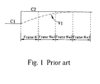
- Fig.1 is a timing diagram of the pixel voltage and the transmission rate V1 according to a prior art LCD.
- the pixel voltage is shown with the straight lines, and the transmission rate V1 is shown with a dotted line.
- frame N means a frame period, and frame N+1, N+2... mean the following frame periods.
- the pixel voltage is switched from a data voltage C1 to a data voltage C2, due to the physical characteristics of liquid crystal molecules, the liquid crystal molecules cannot be twisted to a predetermined angle within a frame period and fail to perform a predetermined transmission rate.
- the transmission rate V1 cannot reach a predetermined transmission rate until the frame period of frame N+2.
- the delayed switch will cause blurring on the LCD.
- Fig.2 is a timing diagram of the pixel voltage and the transmission rate V2 according to a prior art LCD using an over-driving method.
- an over-driving data voltage C3 is added to accelerate the response speed of the liquid crystal molecules. Since a higher data voltage can obtain a faster response speed of the liquid crystal molecules, the data voltage C3 higher than the data voltage C2 can improve the delayed switch to reach the predetermined transmission rate in a frame period. As Fig.2 shows, the curve of the transmission rate V2 can reach the predetermined transmission rate in frame N.
- Fig.3 is a diagram of a general LCD 30.
- the LCD 30 comprises a liquid crystal panel 31, and the liquid crystal panel 31 comprises a plurality of scan lines 32, a plurality of data lines 34, and a plurality of pixels 36.
- Each pixel 36 is connected to a corresponding scan line 32 and a corresponding data line 34, and each pixel 36 has a switching device 38 and a pixel electrode 39.
- the switching device 38 is connected to the corresponding scan line 32 and the corresponding data line 34.
- the driving method of the LCD 30 provides scan voltages to the scan lines 32 to open the switching devices 38, and data voltages are provided to the data lines 34 and transferred to the pixel electrodes 30 through the switching devices 38.
- scan voltages are provided to the scan lines 32 to open the switching devices 38
- data voltages on the data lines 34 will charge the pixel electrodes 39 through the switch devices 38, and twist the liquid crystal molecules.
- scan voltages on the scan lines 32 are removed to close the switching devices 38, the electrical connections between the data lines 34 and the pixel 36 will be cut and the pixel electrodes 39 will remain charged.
- the scan lines 32 control the switching devices 38 to repeatedly open and close, and thus the pixel electrodes 39 can be repeatedly charged. Different data voltages will cause different twisting angles and show different transmission rates. Hence, the LCD 30 displays different images.
- a driving circuit 40 is utilized for driving the LCD 30 in Fig.3 .
- the driving circuit 40 comprises an image data input terminal 41, a bit processor 42, an image memory 43, a comparison circuit 44, a lookup table (LUT) 45, a multiplexer 46, a data line driving circuit 47, a memory 48, a table selector 49, and a temperature detector 51.
- the image memory 43 is a 16-bit (5,6,5 or 5,5,5) memory having the necessary circuitry to read/write the memory cells.
- the image data input terminal 41 transfers 3 image data (RGB) to the bit processor 42, and each image data is 8 bits for controlling the gray levels of the pixel 30.
- Each color has 256 (2 8 ) gray levels, so the 3 image data need 24 bits (8X3) to determine a RGB image.
- the bit processor 42 is used to extract most significant bits (MSB) of the 3 RGB image data. For example, extracting 5 MSB of the R image data, 6 MSB of the G image data, and 5 MSB of the B image data, and storing the extracted data in the image memory 43. It is of course possible that 5 or other quantities MSB can be extracted from 3 RGB image data as long as the total extracted bits are not more than 16.
- the image data input terminal 41 transfers an 8-bit image data D8 to the bit processor 42.
- the bit processor 42 processes the 8-bit image data D8 and outputs a 6-bit second extracted image data D6 and a current 8-bit image data D8.
- the second extracted image data D6 is the 6 MSB extracted from the current 8-bit image data D8 by the bit processor 42, and the second extracted image data D6 is stored in the image memory 43 to delay a frame period. After delayed a frame period, the second extracted image data D6 is outputted as a first extracted image data D6' .
- the first extracted image data D6' and the second extracted image data D6 received by the comparison circuit 44 belong to different frame cycles as they differ one frame period.
- the bit processor 42 transfers the second extracted image data D6 to the comparison circuit 44 and transfers the current 8-bit image data D8 to the multiplexer 46.
- the image memory 43 transfers the first extracted image data D6' to the comparison circuit 44.
- the first extracted image data D6' and the second extracted image data D6 are compared in the comparison circuit 44.
- a result value of 0 or 1 is determined after comparing the first extracted image data D6' and the second extracted image data D6.
- the result value 0 means that the first extracted image data D6' and the second extracted image data D6 are the same, and the result value 1 means that they are different. Since the first extracted image data D6' and the second extracted image data D6 are extracted from two different 8-bit image data D8, the result value 0 means that the differences between these two 8-bit image data D8 is less than 4.
- the result value of the comparison circuit 44 is 0, and the two corresponding 8-bit image data D8 are 8 ⁇ 11 (00001000 ⁇ 00001011).
- the pixel 36 does not need the over-driving control.
- the result value is 1, the difference between these two 8-bit image data D8 is at least 4 and the pixel 36 needs the over-driving control.
- the pixel 36 needs the over-driving control.
- the lookup table 45 comprises a reference table, and the lookup table 45 is operated in accordance with the reference table.
- Fig.5 which illustrates a reference table 50 of the lookup table 45 in Fig.4 .
- the reference table 50 is recorded with (2 6 x 2 6 ) or (2 5 x 2 5 ) 8-bit image data values 52, and each image data value 52 corresponds to different first extracted image data D6' and second extracted image data D6.
- the result value is 1, meaning the first extracted image data D6' and the second extracted image data D6 are different, the first extracted image data D6' and the second extracted image data D6 are transferred to the lookup table 45.
- the lookup table 45 selects a corresponding 8-bit image data value 52 from the reference table 50 as a first image value D8' according to the first extracted image data D6' and the second extracted image data D6, and transfers the first image value D8' to the multiplexer 46.
- the lookup table 45 selects 25 (00011001) from the reference table 50 as the first image value D8' , and transfers the first image value D8' to the multiplexer 46.
- the result value of the comparison circuit 44 is transferred to the multiplexer 46 to control the operation of the multiplexer 46. If the result value is 0, the multiplexer 46 will output the current 8-bit image data D8. If the result value is 1, the multiplexer 46 will output the over-driving image data D8'.
- the output Dout of the multiplexer 46 is transferred to the data line driving circuit 47, and the data line driving circuit 47 produces a corresponding data voltage in accordance with the output Dout (D8 or D8') of the multiplexer 46.
- the data voltage is applied to the corresponding data line 34 to control the pixel 36.
- the output Dout of the multiplexer 46 will be 10 (00001010) and the data line driving circuit 47 will produce a first data voltage corresponding to the output Dout.
- the over-driving image data D8' outputted by the lookup table 45 will be 255 (11111111)
- the output Dout will be 255
- the data line driving circuit 47 will produce a second data voltage corresponding to the output Dout.
- Fig. 6 shows a similar embodiment of the present invention.
- the bit processor 42 extracts different MSBs of the 8-bit image data D8.
- 5 and 6 MSBs of the 8-bit image data D8 are extracted to be the first extracted image data D5' and the second extracted image data D6 respectively.
- the comparison circuit 44 compares the first extracted image data D5' and the second extracted image data D6 and determines the result value.
- the comparison circuit fills the least significant bits (LSB) of the first extracted image data D5' with 0 and compares the filled first extracted image data D5' with the second extracted image data D6.
- LSB least significant bits
- the LSB of the first extracted image data D5' is filled with 0 so that the filled first extracted image data D5' becomes 14 (001110). Then, 14 (001110) is compared with 10 (001010). Again, if the result value is 0, the pixel 36 does not need the over-driving control. If the result value is 1, the pixel 36 needs the over-driving control.
- the comparison circuit 44 can delete the LSB of the second extracted image data D6 and compare the first extracted image data D5' with the modified second extracted image data D6. For example, if the first extracted image data D5' is 7 (00111) and the second extracted image data D6 is 10 (001010), the LSB of the second extracted image data D6 is deleted, and the modified second extracted image data D6 is 5 (00101). Then, 7 (00111) is compared with 5 (00101). Similarly, if the result value is 0, the pixel 36 does not need the over-driving control. If the result value is 1, the pixel 36 needs the over-driving control.
- the reference table used in the lookup table 45 is different.
- Fig.7 is a reference table 70 used for the lookup table 45 in this situation.
- the reference table 70 is recorded with (2 5 x 2 6 ) 8-bit image data values 72.
- the result value is 1, meaning that the first extracted image data D5' and the second extracted image data D6 are different, the first extracted image data D5' and the second extracted image data D6 are transferred to the lookup table 45.
- the lookup table 45 selects a corresponding 8-bit image data value 72 from the reference table 70 as a first image value D8' according to the first extracted image data D5' and the second extracted image data D6, and transfers the first image value D8' to the multiplexer 46.
- the comparison.circuit 44 can further output a LUT enable signal to the lookup table 45.
- the LUT enable signal will turn on the lookup table 45.
- the LUT enable signal will turn off the lookup table 45.
- the bit processor 42 extracts N and P MSBs of the 8-bit image data D8 to form the first extracted image data and the second extracted image data.
- the combination of (N,P) is (6,6) or (5,6), and can be other suitable values such as (5, 5).
- Fig. 8 and Fig.9 are a block diagram of an embodiment where (N,P) is (5,5), and Fig.9 is a reference table 90 used for the lookup table 45 in Fig.8 .
- the operation where (N,P) is (5, 5) is similar to that where (N,P) is (6,6), and the only difference is whether 5 or 6 MSBs of the 8-bit image data D8 is extracted.
- the first extracted image data D5' and the second extracted image data D5 are both 5-bit image data
- the reference table 90 is stored with (2 5 x 2 5 ) 8-bit image data 92.
- the lookup table 45 selects a corresponding 8-bit image data value 92 from the reference table 90 according to the first extracted image data D5' and the second extracted image data D5 to control the followed operation of the data line driving circuit 47.
- the reference tables in the present invention are built by actually measuring the over-driving voltages needed for properly driving the liquid crystal panel in a frame period.
- the reference tables include all of the over-driving image data that drives the pixels from any gray level to another, so the processor used to expand the brief table is not needed, and the efficiency can be improved.
- the driving circuit and the driving method of the present invention extract LSB or MSB of a general bit length, so the management of the image memory can be more convenient and efficient.
Landscapes
- Engineering & Computer Science (AREA)
- Chemical & Material Sciences (AREA)
- Crystallography & Structural Chemistry (AREA)
- Physics & Mathematics (AREA)
- Computer Hardware Design (AREA)
- General Physics & Mathematics (AREA)
- Theoretical Computer Science (AREA)
- Control Of Indicators Other Than Cathode Ray Tubes (AREA)
Claims (10)
- Procédé de pilotage d'un afficheur à cristaux liquides (30), l'afficheur à cristaux liquides (30) comprenant :un panneau à cristaux liquides (31), le panneau à cristaux liquides (31) comprenant :caractérisé par :une pluralité de lignes de balayage (32) ;une pluralité de lignes de données (34) ; etune pluralité de pixels (36), chaque pixel (36) est connecté à une ligne de balayage correspondante (32) et à une ligne de données correspondante (34), et chaque pixel (36) a un dispositif de commutation (38) connecté à la ligne de balayage correspondante (32) et à la ligne de données correspondante (34) ;le procédé de pilotage comprend :(a) la fourniture continue de tensions de balayage aux lignes de balayage (32) ;(b) la réception d'une donnée d'image à M bit en provenance d'une borne d'entrée de données d'image (41) ;(c) l'extraction de N bits de poids fort de la donnée d'image à M bit afin de former une donnée d'image à N bit, N étant inférieur à M ;(d) le retardement de la donnée d'image à N bit d'une période de trame afin de former une donnée d'image retardée à N bit ;(e) la comparaison des P bits de poids fort d'une donnée d'image à M bit actuelle avec la donnée d'image retardée à N bit afin de déterminer une valeur de résultat ;(f) si la valeur de résultat est égale à une première valeur de résultat, la sélection d'une première valeur d'image (52, 72, 92) à partir d'une table de référence (50, 70, 90) utilisée dans une table de consultation (45) conformément aux P bits de poids fort et à la donnée d'image retardée à N bit et la formation d'une première tension de données selon la première valeur d'image (52, 72, 92), et la fourniture de la première tension de données à la ligne de données correspondante (34) ; et(g) si la valeur de résultat est égale à une seconde valeur de résultat, la formation d'une seconde tension de données conformément à la donnée d'image à M bit actuelle et la fourniture de la seconde tension de données à la ligne de données correspondante (34) ;(f1) si la valeur de résultat est égale à la première valeur de résultat, la sortie d'un signal d'activation de table de consultation mettant en fonction la table de consultation (45) ; et(g1) si la valeur de résultat est égale à la seconde valeur de résultat, la sortie d'un signal d'activation de table de consultation mettant hors fonction la table de consultation (45).
- Procédé de pilotage selon la revendication 1, caractérisé en ce que le procédé de pilotage comprend en outre :(h) la production d'un signal de compensation de température conformément à la température du panneau à cristaux liquides (31) ; et(i) la sélection de la table de référence (50, 70, 90) devant être utilisée dans la table de consultation (45) à l'étape (f) parmi une pluralité de tables (54) conformément au signal de compensation de température.
- Procédé de pilotage selon la revendication 1, caractérisé en ce que la table de référence (50, 70, 90) est enregistrée avec 2N x 2P valeurs d'image (52, 72, 92).
- Procédé de pilotage selon la revendication 1, caractérisé en ce que P est supérieur à N.
- Procédé de pilotage selon la revendication 1, caractérisé en ce que P est égal à N.
- Circuit de pilotage (40) pour piloter un afficheur à cristaux liquides (30), l'afficheur à cristaux liquides (30) comprenant :un panneau à cristaux liquides (31), le panneau à cristaux liquides (31) comprenant :une pluralité de lignes de balayage (32) ;une pluralité de lignes de données (34) ; etune pluralité de pixels (36), chaque pixel (36) est connecté à une ligne de balayage correspondante (32) et à une ligne de données correspondante (34), et chaque pixel (36) a un dispositif de commutation (38) connecté à la ligne de balayage correspondante (32) et à la ligne de données correspondante (34) ;le circuit de pilotage (40) comprend :caractérisé en ce que :un circuit de pilotage de ligne de balayage pour fournir de manière continue des tensions de balayage aux lignes de balayage (32) ;une borne d'entrée de données d'image (41) pour recevoir une donnée d'image à M bit ;un processeur de bit (42) pour extraire N bits de poids fort de la donnée d'image à M bit afin de former une donnée d'image à N bit, N est inférieur à M ;une mémoire d'image (43) pour stocker la donnée d'image à N bit et retarder la donnée d'image à N bit d'une période de trame ;un circuit de comparaison (44) pour comparer P bits de poids fort d'une donnée d'image à M bit actuelle avec la donnée d'image retardée à N bit afin de déterminer une valeur de résultat ;une table de consultation (45) pour sortir une valeur d'image (52, 72, 92) à partir d'une table de référence (50, 70, 90) conformément aux B bits de poids fort et à la donnée d'image retardée à N bit ;un multiplexeur (46) pour sortir la valeur d'image (52, 72, 92) ou sortir la donnée d'image à M bit conformément à la valeur de résultat ; etun circuit de pilotage de ligne de données (47) pour former une tension de données conformément à la sortie du multiplexeur (46), et fournir la tension de données à la ligne de données correspondante (34),le circuit de comparaison (44) sort en outre un signal d'activation de table de consultation vers la table de consultation (45) pour mettre en fonction la table de consultation (45) lorsque le multiplexeur (46) devrait sortir la valeur d'image (52, 72, 92) et pour mettre hors fonction la table de consultation (45) lorsque le multiplexeur (46) devrait sortir la donnée d'image à M bit.
- Circuit de pilotage (40) selon la revendication 6, caractérisé en ce que le circuit de pilotage (40) comprend en outre :un détecteur de température (51) pour détecter la température du panneau à cristaux liquides (31), et produire un signal de compensation de température conformément à la température du panneau à cristaux liquides (31) ;une mémoire (48) pour stocker une pluralité de tables (54) ; etun sélecteur (49) pour sélectionner une table de référence (50, 70, 90) parmi la pluralité de tables (54) stockées dans la mémoire (48) conformément au signal de compensation de température, et transférer la table de référence sélectionnée (50, 70, 90) à la table de consultation (45) pour amener la table de consultation (45) à sortir la valeur d'image (52, 72, 92) conformément à la table de référence sélectionnée (50, 70, 90).
- Circuit de pilotage (40) selon la revendication 6, caractérisé en ce que la table de référence (50, 70, 90) est enregistrée avec 2N x 2P valeurs d'image (52, 72, 92).
- Circuit de pilotage (40) selon la revendication 6, caractérisé en ce que P est supérieur à N.
- Circuit de pilotage (40) selon la revendication 6, caractérisé en ce que P est égal à N.
Priority Applications (1)
| Application Number | Priority Date | Filing Date | Title |
|---|---|---|---|
| EP03025009A EP1528534B1 (fr) | 2003-10-30 | 2003-10-30 | Circuit de commande d'un dispositif d'affichage à cristaux liquides et sa méthode de commande |
Applications Claiming Priority (1)
| Application Number | Priority Date | Filing Date | Title |
|---|---|---|---|
| EP03025009A EP1528534B1 (fr) | 2003-10-30 | 2003-10-30 | Circuit de commande d'un dispositif d'affichage à cristaux liquides et sa méthode de commande |
Publications (2)
| Publication Number | Publication Date |
|---|---|
| EP1528534A1 EP1528534A1 (fr) | 2005-05-04 |
| EP1528534B1 true EP1528534B1 (fr) | 2012-04-18 |
Family
ID=34400502
Family Applications (1)
| Application Number | Title | Priority Date | Filing Date |
|---|---|---|---|
| EP03025009A Expired - Lifetime EP1528534B1 (fr) | 2003-10-30 | 2003-10-30 | Circuit de commande d'un dispositif d'affichage à cristaux liquides et sa méthode de commande |
Country Status (1)
| Country | Link |
|---|---|
| EP (1) | EP1528534B1 (fr) |
Families Citing this family (4)
| Publication number | Priority date | Publication date | Assignee | Title |
|---|---|---|---|---|
| CN100353412C (zh) * | 2005-06-03 | 2007-12-05 | 友达光电股份有限公司 | 像素驱动方法、时序控制器与平面显示器 |
| JP4549944B2 (ja) | 2005-07-27 | 2010-09-22 | 三菱電機株式会社 | 画像処理回路 |
| CN101101735B (zh) * | 2006-07-07 | 2011-07-27 | 奇美电子股份有限公司 | 液晶显示装置及其过度驱动方法 |
| CN108806623B (zh) * | 2018-04-25 | 2021-09-10 | 南京京东方显示技术有限公司 | 过压补偿装置及方法及过压补偿显示装置及方法 |
Citations (1)
| Publication number | Priority date | Publication date | Assignee | Title |
|---|---|---|---|---|
| EP1443486A1 (fr) * | 2001-11-09 | 2004-08-04 | Sharp Corporation | Afficheur a cristaux liquides |
Family Cites Families (6)
| Publication number | Priority date | Publication date | Assignee | Title |
|---|---|---|---|---|
| US5347294A (en) * | 1991-04-17 | 1994-09-13 | Casio Computer Co., Ltd. | Image display apparatus |
| JP3052418B2 (ja) * | 1991-04-17 | 2000-06-12 | カシオ計算機株式会社 | 液晶パネル駆動装置 |
| JP4188566B2 (ja) * | 2000-10-27 | 2008-11-26 | 三菱電機株式会社 | 液晶表示装置の駆動回路および駆動方法 |
| US6771242B2 (en) * | 2001-06-11 | 2004-08-03 | Lg. Philips Lcd Co., Ltd. | Method and apparatus for driving liquid crystal display |
| JP2003084736A (ja) * | 2001-06-25 | 2003-03-19 | Nec Corp | 液晶表示装置 |
| KR100840316B1 (ko) * | 2001-11-26 | 2008-06-20 | 삼성전자주식회사 | 액정 표시 장치 및 그의 구동 방법 |
-
2003
- 2003-10-30 EP EP03025009A patent/EP1528534B1/fr not_active Expired - Lifetime
Patent Citations (1)
| Publication number | Priority date | Publication date | Assignee | Title |
|---|---|---|---|---|
| EP1443486A1 (fr) * | 2001-11-09 | 2004-08-04 | Sharp Corporation | Afficheur a cristaux liquides |
Also Published As
| Publication number | Publication date |
|---|---|
| EP1528534A1 (fr) | 2005-05-04 |
Similar Documents
| Publication | Publication Date | Title |
|---|---|---|
| US7248242B2 (en) | Driving circuit of a liquid crystal display and driving method thereof | |
| US8248339B2 (en) | Display controller and display | |
| US7522140B2 (en) | Liquid crystal display device driving method | |
| TWI251195B (en) | A liquid crystal display for improving dynamic contrast and a method for generating gamma voltages for the liquid crystal display | |
| JP3470095B2 (ja) | 液晶表示装置及びその駆動用回路装置 | |
| US7312777B2 (en) | Liquid crystal display device and driving method thereof | |
| US7148869B2 (en) | Driving circuit of a liquid crystal display and relating driving method | |
| US5635950A (en) | Drive circuit for a display apparatus | |
| JP5100312B2 (ja) | 液晶表示装置及びlcdドライバ | |
| JPH11312977A (ja) | 非線形デジタル―アナログコンバ―タおよびディスプレイ | |
| JP2004226952A (ja) | ディスプレイの反応速度増加装置と駆動方法 | |
| JPH07110666A (ja) | 表示装置の駆動方法 | |
| JPH04365094A (ja) | 液晶表示装置 | |
| EP1528534B1 (fr) | Circuit de commande d'un dispositif d'affichage à cristaux liquides et sa méthode de commande | |
| JPH06332397A (ja) | フラットパネルディスプレイ装置 | |
| JP2012042788A (ja) | 映像制御装置および映像制御方法 | |
| US7453476B2 (en) | Apparatus for driving discharge display panel using dual subfield coding | |
| US7202843B2 (en) | Driving circuit of a liquid crystal display panel and related driving method | |
| EP1538595B1 (fr) | Circuit de commande pour un dispositif d'affichage à cristaux liquides et son procédé de commande | |
| CN106558290A (zh) | 预校正电路 | |
| JP3979498B2 (ja) | 液晶表示器の駆動回路及び駆動方法 | |
| EP1548698A1 (fr) | Circuit de commande d'un dispositif d'affichage à cristaux liquides et sa méthode de commande | |
| JP2002055655A (ja) | ステップ式充放電による低パワーの液晶駆動回路及び駆動方法 |
Legal Events
| Date | Code | Title | Description |
|---|---|---|---|
| PUAI | Public reference made under article 153(3) epc to a published international application that has entered the european phase |
Free format text: ORIGINAL CODE: 0009012 |
|
| 17P | Request for examination filed |
Effective date: 20040924 |
|
| AK | Designated contracting states |
Kind code of ref document: A1 Designated state(s): AT BE BG CH CY CZ DE DK EE ES FI FR GB GR HU IE IT LI LU MC NL PT RO SE SI SK TR |
|
| AX | Request for extension of the european patent |
Extension state: AL LT LV MK |
|
| AKX | Designation fees paid |
Designated state(s): DE FR GB |
|
| 17Q | First examination report despatched |
Effective date: 20080226 |
|
| GRAP | Despatch of communication of intention to grant a patent |
Free format text: ORIGINAL CODE: EPIDOSNIGR1 |
|
| RIN1 | Information on inventor provided before grant (corrected) |
Inventor name: CHIEN, LIANG-CHEN Inventor name: CHEN, CHENG-JUNG Inventor name: SHEN, YUH-REN |
|
| GRAS | Grant fee paid |
Free format text: ORIGINAL CODE: EPIDOSNIGR3 |
|
| GRAA | (expected) grant |
Free format text: ORIGINAL CODE: 0009210 |
|
| AK | Designated contracting states |
Kind code of ref document: B1 Designated state(s): DE FR GB |
|
| REG | Reference to a national code |
Ref country code: GB Ref legal event code: FG4D |
|
| REG | Reference to a national code |
Ref country code: DE Ref legal event code: R096 Ref document number: 60340629 Country of ref document: DE Effective date: 20120614 |
|
| PLBE | No opposition filed within time limit |
Free format text: ORIGINAL CODE: 0009261 |
|
| STAA | Information on the status of an ep patent application or granted ep patent |
Free format text: STATUS: NO OPPOSITION FILED WITHIN TIME LIMIT |
|
| 26N | No opposition filed |
Effective date: 20130121 |
|
| REG | Reference to a national code |
Ref country code: DE Ref legal event code: R097 Ref document number: 60340629 Country of ref document: DE Effective date: 20130121 |
|
| GBPC | Gb: european patent ceased through non-payment of renewal fee |
Effective date: 20121030 |
|
| REG | Reference to a national code |
Ref country code: FR Ref legal event code: ST Effective date: 20130628 |
|
| PG25 | Lapsed in a contracting state [announced via postgrant information from national office to epo] |
Ref country code: GB Free format text: LAPSE BECAUSE OF NON-PAYMENT OF DUE FEES Effective date: 20121030 |
|
| PG25 | Lapsed in a contracting state [announced via postgrant information from national office to epo] |
Ref country code: FR Free format text: LAPSE BECAUSE OF NON-PAYMENT OF DUE FEES Effective date: 20121031 |
|
| PGFP | Annual fee paid to national office [announced via postgrant information from national office to epo] |
Ref country code: DE Payment date: 20151029 Year of fee payment: 13 |
|
| REG | Reference to a national code |
Ref country code: DE Ref legal event code: R119 Ref document number: 60340629 Country of ref document: DE |
|
| PG25 | Lapsed in a contracting state [announced via postgrant information from national office to epo] |
Ref country code: DE Free format text: LAPSE BECAUSE OF NON-PAYMENT OF DUE FEES Effective date: 20170503 |