EP1527463B1 - Planar inductance - Google Patents
Planar inductance Download PDFInfo
- Publication number
- EP1527463B1 EP1527463B1 EP03771228A EP03771228A EP1527463B1 EP 1527463 B1 EP1527463 B1 EP 1527463B1 EP 03771228 A EP03771228 A EP 03771228A EP 03771228 A EP03771228 A EP 03771228A EP 1527463 B1 EP1527463 B1 EP 1527463B1
- Authority
- EP
- European Patent Office
- Prior art keywords
- winding
- planar
- planar inductance
- conductors
- eye
- Prior art date
- Legal status (The legal status is an assumption and is not a legal conclusion. Google has not performed a legal analysis and makes no representation as to the accuracy of the status listed.)
- Expired - Lifetime
Links
Images
Classifications
-
- H—ELECTRICITY
- H01—ELECTRIC ELEMENTS
- H01F—MAGNETS; INDUCTANCES; TRANSFORMERS; SELECTION OF MATERIALS FOR THEIR MAGNETIC PROPERTIES
- H01F17/00—Fixed inductances of the signal type
- H01F17/0006—Printed inductances
-
- H—ELECTRICITY
- H01—ELECTRIC ELEMENTS
- H01F—MAGNETS; INDUCTANCES; TRANSFORMERS; SELECTION OF MATERIALS FOR THEIR MAGNETIC PROPERTIES
- H01F17/00—Fixed inductances of the signal type
- H01F17/0006—Printed inductances
- H01F2017/0073—Printed inductances with a special conductive pattern, e.g. flat spiral
-
- H—ELECTRICITY
- H01—ELECTRIC ELEMENTS
- H01F—MAGNETS; INDUCTANCES; TRANSFORMERS; SELECTION OF MATERIALS FOR THEIR MAGNETIC PROPERTIES
- H01F21/00—Variable inductances or transformers of the signal type
- H01F21/12—Variable inductances or transformers of the signal type discontinuously variable, e.g. tapped
- H01F2021/125—Printed variable inductor with taps, e.g. for VCO
-
- H—ELECTRICITY
- H01—ELECTRIC ELEMENTS
- H01F—MAGNETS; INDUCTANCES; TRANSFORMERS; SELECTION OF MATERIALS FOR THEIR MAGNETIC PROPERTIES
- H01F27/00—Details of transformers or inductances, in general
- H01F27/34—Special means for preventing or reducing unwanted electric or magnetic effects, e.g. no-load losses, reactive currents, harmonics, oscillations, leakage fields
- H01F27/346—Preventing or reducing leakage fields
Definitions
- the invention relates to a planar inductance, in particular for monolithic HF oscillators with planar spiral windings.
- the windings are in the form of essentially closed loops, e.g. any polygons that can assume an elliptical form in the boundary area, or may also be circular in shape, wherein, for connection of the power supply lines, the intersecting winding ends form conductor sections running, in sections, in parallel with each other and carrying current in the same direction.
- the disadvantage of these known structures consists in the fact that a strong magnetic field component evolves outside the winding loop.
- transceiver ICs in mobile communications or in data transmission technology, which comprise further magnetic elements internally or in the external wiring, including parasitic elements if applicable - as is the case in interface circuits for LNAs, for example - interfering couplings may occur with a spiral inductance of this kind. In its turn, this may express itself in undesired oscillations, excessively high crosstalk of the relevant frequency components or similar.
- each winding is in the form of an "eight" with three cross-conductors carrying current in the same direction and running between two loops.
- each spiral winding comprises two loops, one of which carries current clockwise and the other counterclockwise
- the surface requirement is similar to that for the known structures, and roughly identical inductance and performance factor values arise.
- the opposing magnetic flow directions in the two loops of the winding ensure that the greater part of the magnetic flow concentrates around the three central cross-conductors.
- the magnetic dipoles of the mutual windings lead to a good local positioning of the magnetic field components. Outside the windings, therefore, the field is considerably reduced in comparison with the structures used hitherto.
- planar inductance in accordance with the invention may, of course, also be in the form of multiple windings.
- each eye of the winding may be equipped with multiple windings, arranged spirally inside one another, the inner ends of which are joined together.
- the eye of the winding from which the supply lines depart is arranged to be smaller than the other eye, wherein, to this end, an additional metallization plane may be provided, if appropriate, and the central conductors are, in part, located one above the other.
- the US - A - 5 245 307 discloses a planar inductance with windings in the form of an eight. However, from three cross conductors running between two loops only two are carrying current in the same direction, while the third is carrying current perpendicular to the direction of the only two. According to the document WO098/05048 cross conductors carrying current in the same direction only occur between plural loops, that is at least three loops.
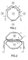
- the winding for a planar inductance in accordance with another prior art as shown in Fig. 1 comprises a ring-shaped loop 1, the ends 2 and 3 of which, crossing over each other, are routed outwards and joined to the power supply lines 4 and 5, or to further loops in the case of multiple windings.
- a strong magnetic field is created outside of the actual winding 1, which - as explained in detail above - has an interfering effect in many application instances.
- a modified structure is depicted, as shown in Fig. 2 , with its winding 1 in the form of a figure "8" with two loops 1a and 1b, wherein three cross-conductors 6 to 8, carrying current in the same direction, are formed between the two loops 1a and 1b.
- These cross-conductors 6 to 8 are located parallel with each other, wherein the top cross-conductor 8 and the bottom cross-conductor 6 are joined on opposite sides to the power supply lines 4 and 5. It hereby goes without saying that crossovers of the planar spiral windings are, of course, insulated.
- the magnetic dipoles of the opposed-direction winding loops 1a and 1b give rise to an extremely good local positioning of the magnetic field components, so that virtually no appreciable magnetic field components any longer occur outside of the winding loops.
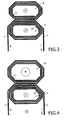
- Fig. 3 shows an example of embodiment of a planar inductance with multiple windings.
- the conductor layout is arranged in such a way that, starting from supply line 5 of the bottom eye 9, the top eye 10 is firstly wound in such a way that the conductor tracks are arranged spirally inside each other.
- the end 11 of the inner winding of the top eye 10 is joined to the end 12 of the inner winding of the bottom eye 9.
- the top eye 10 of the planar inductance is arranged to be larger.
Landscapes
- Engineering & Computer Science (AREA)
- Power Engineering (AREA)
- Microelectronics & Electronic Packaging (AREA)
- Coils Or Transformers For Communication (AREA)
- Semiconductor Integrated Circuits (AREA)
- Coils Of Transformers For General Uses (AREA)
Description
- The invention relates to a planar inductance, in particular for monolithic HF oscillators with planar spiral windings.
- Normally, in the planar inductances known hitherto, the windings are in the form of essentially closed loops, e.g. any polygons that can assume an elliptical form in the boundary area, or may also be circular in shape, wherein, for connection of the power supply lines, the intersecting winding ends form conductor sections running, in sections, in parallel with each other and carrying current in the same direction. The disadvantage of these known structures consists in the fact that a strong magnetic field component evolves outside the winding loop. In the case of integrated circuits, such as transceiver ICs in mobile communications or in data transmission technology, which comprise further magnetic elements internally or in the external wiring, including parasitic elements if applicable - as is the case in interface circuits for LNAs, for example - interfering couplings may occur with a spiral inductance of this kind. In its turn, this may express itself in undesired oscillations, excessively high crosstalk of the relevant frequency components or similar.
- It is therefore an object of the invention to create a planar inductance which, with a structure of similar simplicity to the planar inductances known hitherto, has a reduced magnetic field component outside the windings.
- To achieve this object, the invention provides that each winding is in the form of an "eight" with three cross-conductors carrying current in the same direction and running between two loops.
- Thanks to the design in accordance with the invention, in which each spiral winding comprises two loops, one of which carries current clockwise and the other counterclockwise, the surface requirement is similar to that for the known structures, and roughly identical inductance and performance factor values arise. The opposing magnetic flow directions in the two loops of the winding ensure that the greater part of the magnetic flow concentrates around the three central cross-conductors. The magnetic dipoles of the mutual windings lead to a good local positioning of the magnetic field components. Outside the windings, therefore, the field is considerably reduced in comparison with the structures used hitherto. Measurement results of a self-mixing effect between a fully integrated RF-VCO and a high-frequency receiving circuit, brought about by these magnetic field components, indicate a reduction of around 10 dB for the new structure as compared with the one used hitherto. Finally, it is also within the scope of the invention that the cross-conductors are located parallel with each other, and the top and bottom ones are joined to the power supply lines on opposite sides. These cross-conductors may also be located one above the other.
- The planar inductance in accordance with the invention may, of course, also be in the form of multiple windings. To this end, in an embodiment of the invention, each eye of the winding may be equipped with multiple windings, arranged spirally inside one another, the inner ends of which are joined together.
- To compensate the magnetic field of the supply lines, it may further be provided that the eye of the winding from which the supply lines depart is arranged to be smaller than the other eye, wherein, to this end, an additional metallization plane may be provided, if appropriate, and the central conductors are, in part, located one above the other.
- The invention will be further described with reference to examples of embodiments shown in the drawings, to which, however, the invention is not restricted.
-
Fig. 1 shows a representation of a typical planar inductance in accordance with the prior art. -
Fig. 2 shows a representation of the structure of a planar inductance in accordance with the invention. -
Figs. 3 to 5 show examples of embodiments of a planar inductance with multiple windings. - The
US - A - 5 245 307 discloses a planar inductance with windings in the form of an eight. However, from three cross conductors running between two loops only two are carrying current in the same direction, while the third is carrying current perpendicular to the direction of the only two. According to the documentWO098/05048 - The winding for a planar inductance in accordance with another prior art as shown in
Fig. 1 comprises a ring-shaped loop 1, theends power supply lines actual winding 1, which - as explained in detail above - has an interfering effect in many application instances. - In accordance with the invention, therefore, a modified structure is depicted, as shown in
Fig. 2 , with its winding 1 in the form of a figure "8" with twoloops cross-conductors 6 to 8, carrying current in the same direction, are formed between the twoloops cross-conductors 6 to 8 are located parallel with each other, wherein thetop cross-conductor 8 and thebottom cross-conductor 6 are joined on opposite sides to thepower supply lines - The magnetic dipoles of the opposed-
direction winding loops -
Fig. 3 shows an example of embodiment of a planar inductance with multiple windings. Here, the conductor layout is arranged in such a way that, starting fromsupply line 5 of thebottom eye 9, thetop eye 10 is firstly wound in such a way that the conductor tracks are arranged spirally inside each other. Theend 11 of the inner winding of thetop eye 10 is joined to theend 12 of the inner winding of thebottom eye 9. - To compensate the magnetic field of
supply lines Fig. 4 , thetop eye 10 of the planar inductance is arranged to be larger. - In the embodiment example shown in
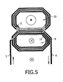
Fig. 5 , in which thetop eye 10, i.e. the eye withoutsupply lines
Claims (5)
- A planar inductance, in particular for monolithic HF oscillators, with planar spiral windings, wherein winding (1) is in the form of an "eight" with three cross-conductors (6, 7, 8) carrying current in the same direction and running between two loops (1a, 1b).
- A planar inductance as claimed in claim 1, characterized in that the cross-conductors (6, 7, 8) are located parallel with each other, and the top (8) and bottom (6) ones are joined to the power supply lines (4, 5) on opposite sides.
- A planar inductance as claimed in claim 1 or 2, characterized in that each eye (9, 10) of the winding is equipped with multiple windings, arranged spirally inside one another, the inner ends (11, 12) of which are joined together.
- A planar inductance as claimed in claim 3, characterized in that the eye (9) of the winding adjacent to which the supply lines (4, 5) run is arranged to be smaller than the other eye (10) in order to compensate the magnetic field of the supply lines (4, 5).
- A planar inductance as claimed in claim 4, characterized in that an additional metallization plane is provided, and the central cross-conductors are, in part, located one above the other.
Applications Claiming Priority (3)
| Application Number | Priority Date | Filing Date | Title |
|---|---|---|---|
| DE10233980 | 2002-07-25 | ||
| DE10233980A DE10233980A1 (en) | 2002-07-25 | 2002-07-25 | planar inductor |
| PCT/IB2003/003227 WO2004012213A1 (en) | 2002-07-25 | 2003-07-16 | Planar inductance |
Publications (2)
| Publication Number | Publication Date |
|---|---|
| EP1527463A1 EP1527463A1 (en) | 2005-05-04 |
| EP1527463B1 true EP1527463B1 (en) | 2012-09-05 |
Family
ID=30128411
Family Applications (1)
| Application Number | Title | Priority Date | Filing Date |
|---|---|---|---|
| EP03771228A Expired - Lifetime EP1527463B1 (en) | 2002-07-25 | 2003-07-16 | Planar inductance |
Country Status (7)
| Country | Link |
|---|---|
| US (1) | US7642891B2 (en) |
| EP (1) | EP1527463B1 (en) |
| JP (1) | JP2005534184A (en) |
| CN (1) | CN100338698C (en) |
| AU (1) | AU2003247070A1 (en) |
| DE (1) | DE10233980A1 (en) |
| WO (1) | WO2004012213A1 (en) |
Families Citing this family (58)
| Publication number | Priority date | Publication date | Assignee | Title |
|---|---|---|---|---|
| KR101005264B1 (en) * | 2003-07-26 | 2011-01-04 | 삼성전자주식회사 | Symmetric Inductor Device |
| US7151430B2 (en) * | 2004-03-03 | 2006-12-19 | Telefonaktiebolaget Lm Ericsson (Publ) | Method of and inductor layout for reduced VCO coupling |
| JP2005327931A (en) * | 2004-05-14 | 2005-11-24 | Sony Corp | Integrated inductor and receiving circuit using the same |
| US7432794B2 (en) * | 2004-08-16 | 2008-10-07 | Telefonaktiebolaget L M Ericsson (Publ) | Variable integrated inductor |
| WO2006075217A1 (en) * | 2005-01-12 | 2006-07-20 | Koninklijke Philips Electronics N.V. | Inductor |
| WO2006105184A1 (en) * | 2005-03-30 | 2006-10-05 | Silicon Laboratories Inc. | Magnetically differential inductors and associated methods |
| US7955886B2 (en) | 2005-03-30 | 2011-06-07 | Silicon Laboratories Inc. | Apparatus and method for reducing interference |
| WO2008007307A1 (en) * | 2006-07-07 | 2008-01-17 | Nxp B.V. | Programmable inductor |
| DE102007027612B4 (en) * | 2007-06-12 | 2009-04-02 | Atmel Duisburg Gmbh | Monolithic integrated inductance |
| US8049588B2 (en) * | 2007-11-21 | 2011-11-01 | Panasonic Corporation | Coil device |
| WO2009101550A1 (en) | 2008-02-14 | 2009-08-20 | Nxp B.V. | Method of correction of network synchronisation |
| JP2009206445A (en) * | 2008-02-29 | 2009-09-10 | Goto Denshi Kk | Alpha-turn coil |
| WO2009125324A1 (en) * | 2008-04-10 | 2009-10-15 | Nxp B.V. | 8-shaped inductor |
| US8421577B2 (en) | 2008-04-21 | 2013-04-16 | Nxp B.V. | Planar inductive unit and an electronic device comprising a planar inductive unit |
| GB2492872B (en) * | 2008-08-29 | 2013-05-01 | Cambridge Silicon Radio Ltd | Inductor structure |
| GB2462885B (en) | 2008-08-29 | 2013-03-27 | Cambridge Silicon Radio Ltd | Inductor structure |
| EP2273613A1 (en) | 2009-07-07 | 2011-01-12 | Nxp B.V. | Magnetic shield layout, semiconductor device and application |
| EP2421011A1 (en) | 2010-08-19 | 2012-02-22 | Nxp B.V. | Symmetrical inductor |
| US9196409B2 (en) * | 2010-12-06 | 2015-11-24 | Nxp, B. V. | Integrated circuit inductors |
| US8576039B2 (en) * | 2011-12-06 | 2013-11-05 | Cambridge Silicon Radio Limited | Inductor structure |
| DE102012112571B3 (en) | 2012-12-18 | 2014-06-05 | Epcos Ag | circuitry |
| CN103107166A (en) * | 2013-01-23 | 2013-05-15 | 华中科技大学 | Inductor and wireless coupling communication system in three-dimensional stack packaging chip |
| US9755671B2 (en) | 2013-08-01 | 2017-09-05 | Qorvo Us, Inc. | VSWR detector for a tunable filter structure |
| US9705478B2 (en) | 2013-08-01 | 2017-07-11 | Qorvo Us, Inc. | Weakly coupled tunable RF receiver architecture |
| US9444417B2 (en) | 2013-03-15 | 2016-09-13 | Qorvo Us, Inc. | Weakly coupled RF network based power amplifier architecture |
| US9294046B2 (en) | 2013-03-15 | 2016-03-22 | Rf Micro Devices (Cayman Islands), Ltd. | RF power amplifier with PM feedback linearization |
| US9780756B2 (en) | 2013-08-01 | 2017-10-03 | Qorvo Us, Inc. | Calibration for a tunable RF filter structure |
| US12224096B2 (en) | 2013-03-15 | 2025-02-11 | Qorvo Us, Inc. | Advanced 3D inductor structures with confined magnetic field |
| US9899133B2 (en) | 2013-08-01 | 2018-02-20 | Qorvo Us, Inc. | Advanced 3D inductor structures with confined magnetic field |
| US9455680B2 (en) | 2013-06-06 | 2016-09-27 | Qorvo Us, Inc. | Tunable RF filter structure formed by a matrix of weakly coupled resonators |
| US9871499B2 (en) | 2013-03-15 | 2018-01-16 | Qorvo Us, Inc. | Multi-band impedance tuners using weakly-coupled LC resonators |
| US9685928B2 (en) | 2013-08-01 | 2017-06-20 | Qorvo Us, Inc. | Interference rejection RF filters |
| US9825656B2 (en) | 2013-08-01 | 2017-11-21 | Qorvo Us, Inc. | Weakly coupled tunable RF transmitter architecture |
| US9774311B2 (en) | 2013-03-15 | 2017-09-26 | Qorvo Us, Inc. | Filtering characteristic adjustments of weakly coupled tunable RF filters |
| US9628045B2 (en) | 2013-08-01 | 2017-04-18 | Qorvo Us, Inc. | Cooperative tunable RF filters |
| US9859863B2 (en) | 2013-03-15 | 2018-01-02 | Qorvo Us, Inc. | RF filter structure for antenna diversity and beam forming |
| JP5979233B2 (en) * | 2013-03-29 | 2016-08-24 | 株式会社村田製作所 | Multilayer coil parts and matching circuit |
| DE102013104842B4 (en) * | 2013-05-10 | 2015-11-12 | Epcos Ag | Miniaturized RF component with reduced coupling |
| US9705542B2 (en) | 2013-06-06 | 2017-07-11 | Qorvo Us, Inc. | Reconfigurable RF filter |
| US9800282B2 (en) | 2013-06-06 | 2017-10-24 | Qorvo Us, Inc. | Passive voltage-gain network |
| US9780817B2 (en) | 2013-06-06 | 2017-10-03 | Qorvo Us, Inc. | RX shunt switching element-based RF front-end circuit |
| US9966981B2 (en) | 2013-06-06 | 2018-05-08 | Qorvo Us, Inc. | Passive acoustic resonator based RF receiver |
| EP2887364B1 (en) | 2013-12-18 | 2017-06-07 | Nxp B.V. | Integrated transformer |
| DE102014202128A1 (en) | 2014-02-06 | 2015-08-06 | Siemens Aktiengesellschaft | inductor |
| CN105321932B (en) * | 2014-07-03 | 2018-09-14 | 瑞昱半导体股份有限公司 | It can inhibit the inductance capacitance resonant cavity and its manufacturing method that self electromagnetism radiates |
| TWI553676B (en) | 2015-07-07 | 2016-10-11 | 瑞昱半導體股份有限公司 | Structure of planar transformer and balun |
| US10796835B2 (en) | 2015-08-24 | 2020-10-06 | Qorvo Us, Inc. | Stacked laminate inductors for high module volume utilization and performance-cost-size-processing-time tradeoff |
| TWI591800B (en) * | 2015-10-06 | 2017-07-11 | 瑞昱半導體股份有限公司 | Integrated inductor structure and integrated transformer structure |
| TWI579997B (en) | 2016-01-07 | 2017-04-21 | 瑞昱半導體股份有限公司 | Integral inductor structure |
| CN105761881A (en) * | 2016-05-20 | 2016-07-13 | 浙江求缺科技有限公司 | Planar winding coil for double-column magnetic core structure |
| TWI627644B (en) | 2016-08-05 | 2018-06-21 | 瑞昱半導體股份有限公司 | Semiconductor component |
| TWI632657B (en) | 2016-08-05 | 2018-08-11 | 瑞昱半導體股份有限公司 | Semiconductor component |
| CN107731780B (en) * | 2016-08-12 | 2019-09-17 | 瑞昱半导体股份有限公司 | Semiconductor device with a plurality of semiconductor chips |
| CN107731781B (en) * | 2016-08-12 | 2019-09-17 | 瑞昱半导体股份有限公司 | Semiconductor device with a plurality of semiconductor chips |
| US11139238B2 (en) | 2016-12-07 | 2021-10-05 | Qorvo Us, Inc. | High Q factor inductor structure |
| US10068699B1 (en) * | 2017-03-01 | 2018-09-04 | Realtek Semiconductor Corp. | Integrated inductor and fabrication method thereof |
| GB2576874A (en) * | 2018-08-24 | 2020-03-11 | Bombardier Primove Gmbh | Conductor arrangement, system and methods for an inductive power transfer |
| JP7003955B2 (en) * | 2019-03-19 | 2022-02-04 | 株式会社豊田中央研究所 | Noise filter |
Family Cites Families (17)
| Publication number | Priority date | Publication date | Assignee | Title |
|---|---|---|---|---|
| US2471777A (en) * | 1946-03-27 | 1949-05-31 | Rca Corp | Method of making ultra high frequency inductors |
| JPS4997337U (en) * | 1972-12-15 | 1974-08-22 | ||
| JPS5819200B2 (en) * | 1977-12-23 | 1983-04-16 | パイオニア株式会社 | Moving coil type cartridge |
| US4201965A (en) * | 1978-06-29 | 1980-05-06 | Rca Corporation | Inductance fabricated on a metal base printed circuit board |
| JPS5795609A (en) * | 1980-12-05 | 1982-06-14 | Kangiyou Denki Kiki Kk | Sheet coil |
| JPS59132604A (en) * | 1983-01-20 | 1984-07-30 | Nec Corp | Laminated inductor |
| DE3912840A1 (en) | 1989-04-19 | 1990-10-25 | Foerster Inst Dr Friedrich | SEARCH COIL ARRANGEMENT FOR AN INDUCTIVE SEARCH DEVICE |
| DE3920081A1 (en) * | 1989-06-20 | 1991-01-03 | Foerster Inst Dr Friedrich | SEARCH COIL ARRANGEMENT |
| JPH03219609A (en) * | 1990-01-24 | 1991-09-27 | Murata Mfg Co Ltd | Laminated-type common-mode choke coil |
| JP3141562B2 (en) * | 1992-05-27 | 2001-03-05 | 富士電機株式会社 | Thin film transformer device |
| JPH0653044A (en) * | 1992-07-31 | 1994-02-25 | Nippon Steel Corp | Thin inductor or thin transformer and their manufacture |
| AU3597897A (en) * | 1996-07-29 | 1998-02-20 | Motorola, Inc. | Low radiation planar inductor/transformer and method |
| JP4138956B2 (en) * | 1998-07-31 | 2008-08-27 | Tdk株式会社 | Coil parts |
| JP2000101025A (en) * | 1998-09-17 | 2000-04-07 | Kanagawa Prefecture | Integrated circuit with magnetic element |
| JP3765366B2 (en) * | 1999-05-19 | 2006-04-12 | 富士電機デバイステクノロジー株式会社 | Planar magnetic element integrated semiconductor device |
| DE19958908A1 (en) * | 1999-12-07 | 2001-06-21 | Infineon Technologies Ag | Circuit arrangement for direct modulation |
| US7151430B2 (en) * | 2004-03-03 | 2006-12-19 | Telefonaktiebolaget Lm Ericsson (Publ) | Method of and inductor layout for reduced VCO coupling |
-
2002
- 2002-07-25 DE DE10233980A patent/DE10233980A1/en not_active Withdrawn
-
2003
- 2003-07-16 JP JP2004524018A patent/JP2005534184A/en active Pending
- 2003-07-16 US US10/521,854 patent/US7642891B2/en not_active Expired - Lifetime
- 2003-07-16 AU AU2003247070A patent/AU2003247070A1/en not_active Abandoned
- 2003-07-16 CN CNB038178400A patent/CN100338698C/en not_active Expired - Lifetime
- 2003-07-16 EP EP03771228A patent/EP1527463B1/en not_active Expired - Lifetime
- 2003-07-16 WO PCT/IB2003/003227 patent/WO2004012213A1/en not_active Ceased
Also Published As
| Publication number | Publication date |
|---|---|
| WO2004012213A1 (en) | 2004-02-05 |
| EP1527463A1 (en) | 2005-05-04 |
| US20050237144A1 (en) | 2005-10-27 |
| CN1672223A (en) | 2005-09-21 |
| AU2003247070A1 (en) | 2004-02-16 |
| US7642891B2 (en) | 2010-01-05 |
| DE10233980A1 (en) | 2004-02-12 |
| JP2005534184A (en) | 2005-11-10 |
| CN100338698C (en) | 2007-09-19 |
Similar Documents
| Publication | Publication Date | Title |
|---|---|---|
| EP1527463B1 (en) | Planar inductance | |
| US7796006B2 (en) | Suspension inductor devices | |
| CN101185146B (en) | Magnetic differential sensor and related method | |
| EP2421011A1 (en) | Symmetrical inductor | |
| US9305697B2 (en) | Integrated transformer | |
| US20010033204A1 (en) | Monolithically intergrated transformer | |
| JP6461437B2 (en) | Noise filter circuit | |
| US20020067235A1 (en) | High Q spiral inductor | |
| US10242791B2 (en) | Coupled-inductor module and voltage regulating module comprising the same | |
| US9508480B2 (en) | Vertical slow-wave symmetric inductor structure for semiconductor devices | |
| US20060254814A1 (en) | Ground shield structure | |
| US20100314713A1 (en) | Integrated Circuit Inductors with Reduced Magnetic Coupling | |
| US7955886B2 (en) | Apparatus and method for reducing interference | |
| US11783991B2 (en) | Inductor device | |
| WO2006105184A1 (en) | Magnetically differential inductors and associated methods | |
| US20230230764A1 (en) | Offset transformer structure | |
| WO2016129199A1 (en) | Structure and wiring substrate | |
| CN215988377U (en) | Inductance structure and radio frequency module | |
| US7943857B2 (en) | Sliced electromagnetic cage for inductors | |
| JP2004095777A (en) | Inductor element | |
| CN110783079B (en) | an inductive structure | |
| JP2006013713A (en) | Line filter | |
| US20250203756A1 (en) | Circuit board module capable of suppressing common mode noise | |
| CN223638193U (en) | An inductor component and an electronic device | |
| CN213071122U (en) | Shielding structure and semiconductor device |
Legal Events
| Date | Code | Title | Description |
|---|---|---|---|
| PUAI | Public reference made under article 153(3) epc to a published international application that has entered the european phase |
Free format text: ORIGINAL CODE: 0009012 |
|
| 17P | Request for examination filed |
Effective date: 20050225 |
|
| AK | Designated contracting states |
Kind code of ref document: A1 Designated state(s): AT BE BG CH CY CZ DE DK EE ES FI FR GB GR HU IE IT LI LU MC NL PT RO SE SI SK TR |
|
| AX | Request for extension of the european patent |
Extension state: AL LT LV MK |
|
| DAX | Request for extension of the european patent (deleted) | ||
| RAP1 | Party data changed (applicant data changed or rights of an application transferred) |
Owner name: PHILIPS INTELLECTUAL PROPERTY & STANDARDS GMBH Owner name: KONINKLIJKE PHILIPS ELECTRONICS N.V. |
|
| RAP1 | Party data changed (applicant data changed or rights of an application transferred) |
Owner name: NXP B.V. |
|
| GRAP | Despatch of communication of intention to grant a patent |
Free format text: ORIGINAL CODE: EPIDOSNIGR1 |
|
| RIN1 | Information on inventor provided before grant (corrected) |
Inventor name: EINZINGER, J., Inventor name: LOTH, ANDREAS, |
|
| GRAS | Grant fee paid |
Free format text: ORIGINAL CODE: EPIDOSNIGR3 |
|
| GRAA | (expected) grant |
Free format text: ORIGINAL CODE: 0009210 |
|
| RAP1 | Party data changed (applicant data changed or rights of an application transferred) |
Owner name: ST-ERICSSON SA |
|
| AK | Designated contracting states |
Kind code of ref document: B1 Designated state(s): AT BE BG CH CY CZ DE DK EE ES FI FR GB GR HU IE IT LI LU MC NL PT RO SE SI SK TR |
|
| REG | Reference to a national code |
Ref country code: GB Ref legal event code: FG4D |
|
| REG | Reference to a national code |
Ref country code: CH Ref legal event code: EP |
|
| REG | Reference to a national code |
Ref country code: AT Ref legal event code: REF Ref document number: 574451 Country of ref document: AT Kind code of ref document: T Effective date: 20120915 |
|
| REG | Reference to a national code |
Ref country code: IE Ref legal event code: FG4D |
|
| REG | Reference to a national code |
Ref country code: DE Ref legal event code: R096 Ref document number: 60342027 Country of ref document: DE Effective date: 20121025 |
|
| REG | Reference to a national code |
Ref country code: NL Ref legal event code: T3 |
|
| REG | Reference to a national code |
Ref country code: AT Ref legal event code: MK05 Ref document number: 574451 Country of ref document: AT Kind code of ref document: T Effective date: 20120905 |
|
| PG25 | Lapsed in a contracting state [announced via postgrant information from national office to epo] |
Ref country code: CY Free format text: LAPSE BECAUSE OF FAILURE TO SUBMIT A TRANSLATION OF THE DESCRIPTION OR TO PAY THE FEE WITHIN THE PRESCRIBED TIME-LIMIT Effective date: 20120905 Ref country code: FI Free format text: LAPSE BECAUSE OF FAILURE TO SUBMIT A TRANSLATION OF THE DESCRIPTION OR TO PAY THE FEE WITHIN THE PRESCRIBED TIME-LIMIT Effective date: 20120905 Ref country code: AT Free format text: LAPSE BECAUSE OF FAILURE TO SUBMIT A TRANSLATION OF THE DESCRIPTION OR TO PAY THE FEE WITHIN THE PRESCRIBED TIME-LIMIT Effective date: 20120905 |
|
| PG25 | Lapsed in a contracting state [announced via postgrant information from national office to epo] |
Ref country code: GR Free format text: LAPSE BECAUSE OF FAILURE TO SUBMIT A TRANSLATION OF THE DESCRIPTION OR TO PAY THE FEE WITHIN THE PRESCRIBED TIME-LIMIT Effective date: 20121206 Ref country code: SE Free format text: LAPSE BECAUSE OF FAILURE TO SUBMIT A TRANSLATION OF THE DESCRIPTION OR TO PAY THE FEE WITHIN THE PRESCRIBED TIME-LIMIT Effective date: 20120905 Ref country code: SI Free format text: LAPSE BECAUSE OF FAILURE TO SUBMIT A TRANSLATION OF THE DESCRIPTION OR TO PAY THE FEE WITHIN THE PRESCRIBED TIME-LIMIT Effective date: 20120905 |
|
| PG25 | Lapsed in a contracting state [announced via postgrant information from national office to epo] |
Ref country code: RO Free format text: LAPSE BECAUSE OF FAILURE TO SUBMIT A TRANSLATION OF THE DESCRIPTION OR TO PAY THE FEE WITHIN THE PRESCRIBED TIME-LIMIT Effective date: 20120905 Ref country code: BE Free format text: LAPSE BECAUSE OF FAILURE TO SUBMIT A TRANSLATION OF THE DESCRIPTION OR TO PAY THE FEE WITHIN THE PRESCRIBED TIME-LIMIT Effective date: 20120905 Ref country code: ES Free format text: LAPSE BECAUSE OF FAILURE TO SUBMIT A TRANSLATION OF THE DESCRIPTION OR TO PAY THE FEE WITHIN THE PRESCRIBED TIME-LIMIT Effective date: 20121216 Ref country code: EE Free format text: LAPSE BECAUSE OF FAILURE TO SUBMIT A TRANSLATION OF THE DESCRIPTION OR TO PAY THE FEE WITHIN THE PRESCRIBED TIME-LIMIT Effective date: 20120905 Ref country code: CZ Free format text: LAPSE BECAUSE OF FAILURE TO SUBMIT A TRANSLATION OF THE DESCRIPTION OR TO PAY THE FEE WITHIN THE PRESCRIBED TIME-LIMIT Effective date: 20120905 |
|
| PG25 | Lapsed in a contracting state [announced via postgrant information from national office to epo] |
Ref country code: SK Free format text: LAPSE BECAUSE OF FAILURE TO SUBMIT A TRANSLATION OF THE DESCRIPTION OR TO PAY THE FEE WITHIN THE PRESCRIBED TIME-LIMIT Effective date: 20120905 Ref country code: PT Free format text: LAPSE BECAUSE OF FAILURE TO SUBMIT A TRANSLATION OF THE DESCRIPTION OR TO PAY THE FEE WITHIN THE PRESCRIBED TIME-LIMIT Effective date: 20130107 |
|
| PLBE | No opposition filed within time limit |
Free format text: ORIGINAL CODE: 0009261 |
|
| STAA | Information on the status of an ep patent application or granted ep patent |
Free format text: STATUS: NO OPPOSITION FILED WITHIN TIME LIMIT |
|
| PG25 | Lapsed in a contracting state [announced via postgrant information from national office to epo] |
Ref country code: DK Free format text: LAPSE BECAUSE OF FAILURE TO SUBMIT A TRANSLATION OF THE DESCRIPTION OR TO PAY THE FEE WITHIN THE PRESCRIBED TIME-LIMIT Effective date: 20120905 Ref country code: BG Free format text: LAPSE BECAUSE OF FAILURE TO SUBMIT A TRANSLATION OF THE DESCRIPTION OR TO PAY THE FEE WITHIN THE PRESCRIBED TIME-LIMIT Effective date: 20121205 |
|
| 26N | No opposition filed |
Effective date: 20130606 |
|
| PG25 | Lapsed in a contracting state [announced via postgrant information from national office to epo] |
Ref country code: IT Free format text: LAPSE BECAUSE OF FAILURE TO SUBMIT A TRANSLATION OF THE DESCRIPTION OR TO PAY THE FEE WITHIN THE PRESCRIBED TIME-LIMIT Effective date: 20120905 |
|
| REG | Reference to a national code |
Ref country code: DE Ref legal event code: R097 Ref document number: 60342027 Country of ref document: DE Effective date: 20130606 |
|
| PG25 | Lapsed in a contracting state [announced via postgrant information from national office to epo] |
Ref country code: MC Free format text: LAPSE BECAUSE OF FAILURE TO SUBMIT A TRANSLATION OF THE DESCRIPTION OR TO PAY THE FEE WITHIN THE PRESCRIBED TIME-LIMIT Effective date: 20120905 |
|
| REG | Reference to a national code |
Ref country code: CH Ref legal event code: PL |
|
| REG | Reference to a national code |
Ref country code: IE Ref legal event code: MM4A |
|
| REG | Reference to a national code |
Ref country code: FR Ref legal event code: ST Effective date: 20140331 |
|
| PG25 | Lapsed in a contracting state [announced via postgrant information from national office to epo] |
Ref country code: CH Free format text: LAPSE BECAUSE OF NON-PAYMENT OF DUE FEES Effective date: 20130731 Ref country code: LI Free format text: LAPSE BECAUSE OF NON-PAYMENT OF DUE FEES Effective date: 20130731 |
|
| PG25 | Lapsed in a contracting state [announced via postgrant information from national office to epo] |
Ref country code: FR Free format text: LAPSE BECAUSE OF NON-PAYMENT OF DUE FEES Effective date: 20130731 |
|
| REG | Reference to a national code |
Ref country code: GB Ref legal event code: 732E Free format text: REGISTERED BETWEEN 20140515 AND 20140521 |
|
| PG25 | Lapsed in a contracting state [announced via postgrant information from national office to epo] |
Ref country code: IE Free format text: LAPSE BECAUSE OF NON-PAYMENT OF DUE FEES Effective date: 20130716 |
|
| REG | Reference to a national code |
Ref country code: DE Ref legal event code: R081 Ref document number: 60342027 Country of ref document: DE Owner name: ERICSSON MODEMS SA, CH Free format text: FORMER OWNER: ST-ERICSSON SA, GENEVE, CH Effective date: 20140723 Ref country code: DE Ref legal event code: R081 Ref document number: 60342027 Country of ref document: DE Owner name: ERICSSON MODEMS SA, CH Free format text: FORMER OWNER: PHILIPS INTELLECTUAL PROPERTY &, KONINKLIJKE PHILIPS ELECTRONICS, , NL Effective date: 20120905 Ref country code: DE Ref legal event code: R081 Ref document number: 60342027 Country of ref document: DE Owner name: ERICSSON MODEMS SA, CH Free format text: FORMER OWNERS: PHILIPS INTELLECTUAL PROPERTY & STANDARDS GMBH, 20099 HAMBURG, DE; KONINKLIJKE PHILIPS ELECTRONICS N.V., EINDHOVEN, NL Effective date: 20120905 Ref country code: DE Ref legal event code: R081 Ref document number: 60342027 Country of ref document: DE Owner name: TELEFONAKTIEBOLAGET L M ERICSSON (PUBL), SE Free format text: FORMER OWNERS: PHILIPS INTELLECTUAL PROPERTY & STANDARDS GMBH, 20099 HAMBURG, DE; KONINKLIJKE PHILIPS ELECTRONICS N.V., EINDHOVEN, NL Effective date: 20120905 Ref country code: DE Ref legal event code: R081 Ref document number: 60342027 Country of ref document: DE Owner name: TELEFONAKTIEBOLAGET L M ERICSSON (PUBL), SE Free format text: FORMER OWNER: ST-ERICSSON SA, GENEVE, CH Effective date: 20140723 |
|
| PG25 | Lapsed in a contracting state [announced via postgrant information from national office to epo] |
Ref country code: TR Free format text: LAPSE BECAUSE OF FAILURE TO SUBMIT A TRANSLATION OF THE DESCRIPTION OR TO PAY THE FEE WITHIN THE PRESCRIBED TIME-LIMIT Effective date: 20120905 |
|
| PG25 | Lapsed in a contracting state [announced via postgrant information from national office to epo] |
Ref country code: HU Free format text: LAPSE BECAUSE OF FAILURE TO SUBMIT A TRANSLATION OF THE DESCRIPTION OR TO PAY THE FEE WITHIN THE PRESCRIBED TIME-LIMIT; INVALID AB INITIO Effective date: 20030716 Ref country code: LU Free format text: LAPSE BECAUSE OF NON-PAYMENT OF DUE FEES Effective date: 20130716 |
|
| REG | Reference to a national code |
Ref country code: GB Ref legal event code: 732E Free format text: REGISTERED BETWEEN 20151001 AND 20151007 |
|
| REG | Reference to a national code |
Ref country code: DE Ref legal event code: R081 Ref document number: 60342027 Country of ref document: DE Owner name: TELEFONAKTIEBOLAGET L M ERICSSON (PUBL), SE Free format text: FORMER OWNER: ERICSSON MODEMS SA, LE GRAND-SACONNEX, CH |
|
| REG | Reference to a national code |
Ref country code: NL Ref legal event code: PD Owner name: TELEFONAKTIEBOLAGET L M ERICSSON (PUBL); SE Free format text: DETAILS ASSIGNMENT: VERANDERING VAN EIGENAAR(S), OVERDRACHT; FORMER OWNER NAME: ST-ERICSSON SA Effective date: 20151023 Ref country code: NL Ref legal event code: HC Owner name: ERICSSON MODEMS SA; CH Free format text: DETAILS ASSIGNMENT: VERANDERING VAN EIGENAAR(S), VERANDERING VAN NAAM VAN DE EIGENAAR(S); FORMER OWNER NAME: ST-ERICSSON AT SA Effective date: 20151023 |
|
| PGFP | Annual fee paid to national office [announced via postgrant information from national office to epo] |
Ref country code: NL Payment date: 20220726 Year of fee payment: 20 |
|
| PGFP | Annual fee paid to national office [announced via postgrant information from national office to epo] |
Ref country code: GB Payment date: 20220727 Year of fee payment: 20 Ref country code: DE Payment date: 20220629 Year of fee payment: 20 |
|
| REG | Reference to a national code |
Ref country code: DE Ref legal event code: R071 Ref document number: 60342027 Country of ref document: DE |
|
| REG | Reference to a national code |
Ref country code: NL Ref legal event code: MK Effective date: 20230715 |
|
| REG | Reference to a national code |
Ref country code: GB Ref legal event code: PE20 Expiry date: 20230715 |
|
| PG25 | Lapsed in a contracting state [announced via postgrant information from national office to epo] |
Ref country code: GB Free format text: LAPSE BECAUSE OF EXPIRATION OF PROTECTION Effective date: 20230715 |