EP1525783B1 - Elektronikgehäuse mit integriertem wärmeverteiler - Google Patents
Elektronikgehäuse mit integriertem wärmeverteiler Download PDFInfo
- Publication number
- EP1525783B1 EP1525783B1 EP03766221A EP03766221A EP1525783B1 EP 1525783 B1 EP1525783 B1 EP 1525783B1 EP 03766221 A EP03766221 A EP 03766221A EP 03766221 A EP03766221 A EP 03766221A EP 1525783 B1 EP1525783 B1 EP 1525783B1
- Authority
- EP
- European Patent Office
- Prior art keywords
- heat spreader
- unit
- panel
- per
- circuit board
- Prior art date
- Legal status (The legal status is an assumption and is not a legal conclusion. Google has not performed a legal analysis and makes no representation as to the accuracy of the status listed.)
- Expired - Lifetime
Links
Images
Classifications
-
- H—ELECTRICITY
- H05—ELECTRIC TECHNIQUES NOT OTHERWISE PROVIDED FOR
- H05K—PRINTED CIRCUITS; CASINGS OR CONSTRUCTIONAL DETAILS OF ELECTRIC APPARATUS; MANUFACTURE OF ASSEMBLAGES OF ELECTRICAL COMPONENTS
- H05K5/00—Casings, cabinets or drawers for electric apparatus
- H05K5/06—Hermetically-sealed casings
- H05K5/064—Hermetically-sealed casings sealed by potting, e.g. waterproof resin poured in a rigid casing
-
- H—ELECTRICITY
- H05—ELECTRIC TECHNIQUES NOT OTHERWISE PROVIDED FOR
- H05K—PRINTED CIRCUITS; CASINGS OR CONSTRUCTIONAL DETAILS OF ELECTRIC APPARATUS; MANUFACTURE OF ASSEMBLAGES OF ELECTRICAL COMPONENTS
- H05K7/00—Constructional details common to different types of electric apparatus
- H05K7/20—Modifications to facilitate cooling, ventilating, or heating
- H05K7/2039—Modifications to facilitate cooling, ventilating, or heating characterised by the heat transfer by conduction from the heat generating element to a dissipating body
- H05K7/20436—Inner thermal coupling elements in heat dissipating housings, e.g. protrusions or depressions integrally formed in the housing
- H05K7/20445—Inner thermal coupling elements in heat dissipating housings, e.g. protrusions or depressions integrally formed in the housing the coupling element being an additional piece, e.g. thermal standoff
- H05K7/20463—Filling compound, e.g. potted resin
-
- H—ELECTRICITY
- H05—ELECTRIC TECHNIQUES NOT OTHERWISE PROVIDED FOR
- H05K—PRINTED CIRCUITS; CASINGS OR CONSTRUCTIONAL DETAILS OF ELECTRIC APPARATUS; MANUFACTURE OF ASSEMBLAGES OF ELECTRICAL COMPONENTS
- H05K3/00—Apparatus or processes for manufacturing printed circuits
- H05K3/22—Secondary treatment of printed circuits
- H05K3/28—Applying non-metallic protective coatings
- H05K3/284—Applying non-metallic protective coatings for encapsulating mounted components
Definitions
- the present invention relates to an electronics housing, in particular an electronics housing for a transmitter.
- European patent no. 0 920 789 B1 discloses a heat sink having a substantially planar metallic heat sink disposed between two thin layers of electrically insulating and thermally conductive potting compound at a small distance parallel to the circuit board.
- the metallic heat sink continues in its edge region in a heat-conducting tongue, which is led out of the potting compound and connected to a sufficiently large thermal mass, which is arranged laterally of the circuit board, whereby the waste heat is dissipated parallel to the circuit board.
- the metallic heat sink pores which are penetrated by the potting compound.
- the device described is disadvantageous in that when the cross section of the heat sink perpendicular to the direction of the heat flow is very small and is additionally reduced by the pores.
- the construction of the heat-conducting tongue and its connection to the thermal mass is very expensive.
- the European patent EP 1 182 768 discloses a device according to the preamble of claim 1.
- the basis of the solution according to the invention is the consideration that it is not important to reduce the amount of heat emitted via a housing wall, but only to distribute the heat sufficiently homogeneous over the surface of the housing wall.
- the device comprises an electronics housing which defines an interior space; at least one printed circuit board, which is arranged in the interior and is equipped at least on a first surface with electronic components, wherein the first surface facing a first wall of the electronics housing and the interior filled at least between the first surface of the circuit board and the first wall with a potting compound is, whereby waste heat of the electronic components can be derived to the first wall; wherein in the sealing compound between the circuit board and the first wall, a planar heat spreader is embedded, which faces with its front side of the first wall and with its rear side of the circuit board, and which has a greater specific thermal conductivity than the potting compound, whereby inhomogeneous temperature distributions along the surface the first wall be significantly weakened.
- the heat spreader may be, for example, a thin metal layer, foil, or plate, such as copper.
- the strength of the metal plate results for the skilled person from the amount of heat to be distributed. In most applications, thicknesses of not more than about 1 mm, preferably not more than 0.4 mm, more preferably between 0.05 mm and 0.2 mm are sufficient.
- the heat spreader preferably covers at least the area of the printed circuit board in which those components are arranged which generate substantial portions of the waste heat which occurs.
- a planar heat spreader is preferred, which is arranged parallel to the circuit board and the housing wall.
- the heat spreader can be either planar or curved, wherein the degree of curvature is preferably not stronger than the curvature of the housing wall.
- Silgel As a sealing compound currently Silgel is preferred, but there are also other casting compounds suitable, which are electrically insulating and have sufficient thermal conductivity.
- the electronics housing may in particular be the housing of a transmitter, as used, for example, in industrial process measuring technology.
- the invention is particularly suitable for housing in explosion-proof applications, since it is imperative that the temperature of the entire housing surface remains below critical limits.
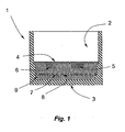
- Transmitter housing 1 shown encloses an inner space 2 in which a printed circuit board 4 is arranged parallel to a first wall 3 of the housing 1.
- the first wall can be, for example, the end face of a cylindrical housing 1.
- electronic or electrical components 5, 6 are arranged, which generate waste heat in operation, which is dissipate in order to avoid overheating of the electronic components 5, 6.
- the interior space 2 at least in the portion between the circuit board 4 and the first wall 3 with a sealing compound 10, preferably Silgel shed.
- a heat spreader 7 is embedded, which is arranged substantially parallel to the printed circuit board 4. The position of the heat spreader 7 spaced from the circuit board and the first wall 3 is defined in this embodiment by stops 9, in which the heat spreader rests in its edge region.
- the heat spreader 7 is preferably a metallic layer, in particular a metallic foil or plate.
- a copper plate is used with a thickness of 0.2 mm.
- the optional opening 8 in the heat spreader 7 allows the passage of the potting compound, which improves the mechanical anchoring of the heat spreader 7.
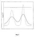
- Fig. 2 explains which schematically shows the profile of the temperature on the outer surface of the housing wall 3 along a line whose projection extends to the plane of the circuit board via the electronic components 5, 6.
- the dashed line shows the temperature profile without a heat spreader in the potting compound and the solid line shows the temperature profile with a heat spreader in the potting compound.
- the heat spreader widens the local temperature maxima and significantly reduces the peak values so that critical limits can be significantly undercut.
- the indication of units has been omitted, since the exact course of the temperature line anyway depends on the geometry of the respective arrangement.
- the peak temperature can be lowered from about 75 ° C to 45 °.
Landscapes
- Engineering & Computer Science (AREA)
- Microelectronics & Electronic Packaging (AREA)
- Physics & Mathematics (AREA)
- Thermal Sciences (AREA)
- Cooling Or The Like Of Electrical Apparatus (AREA)
- Casings For Electric Apparatus (AREA)
- Coupling Device And Connection With Printed Circuit (AREA)
- Laminated Bodies (AREA)
- Cooling Or The Like Of Semiconductors Or Solid State Devices (AREA)
Description
- Die vorliegende Erfindung betrifft ein Elektronikgehäuse insbesondere ein Elektronikgehäuse für einen Meßumformer.
- Bei der Konzeption von elektronischen Geräten ist es wichtig, daß Temperaturspitzen weitgehend vermieden werden, um die Zuverlässigkeit der elektronischen Schaltkreise zu gewährleisten. Insbesondere in explosionsgeschützten Anwendungen ist zu gewährleisten, die Abwärme von elektronischen Bauelementen so abzuführen, daß an keiner Oberfläche eines Gerätes, die Zündtemperatur erreicht wird.
- Der Stand der Technik offenbart insbesondere drucktechnisch hergestellte Wärmesenken auf Leiterplatten, wozu Kramer et al. im Referat Nr. 144 der EPC Conference am11. November 1999 in München einen Überblick geben. Auf einer Leiterplatte gedruckte Wärmepfade haben jedoch einen Flächenbedarf, welcher die Integration elektrischer bzw. elektronischer Bauelemente auf der Leiterplatte beschränkt.
- Das europäische Patent Nr.
0 920 789 B1 offenbart eine Wärmesenke, welche eine im wesentlichen planare metallische Wärmesenke aufweist, die zwischen zwei dünnen Schichten von elektrisch isolierender und thermisch leitender Vergußmasse mit geringem Abstand parallel zur Leiterplatte angeordnet ist. Die metallische Wärmesenke setzt sich in Ihrem Randbereich in einer wärmeleitenden Zunge fort, welche aus der Vergußmasse herausgeführt wird und mit einer hinreichend großen thermischen Masse verbunden ist, welche seitlich von der Leiterplatte angeordnet ist, wodurch die Abwärme parallel zur Leiterplatte abgeführt wird. Zur festen Verankerung der metallischen Wärmesenke in den dünnen Vergußmasseschichten weist die metallische Wärmesenke Poren auf, welche von der Vergußmasse durchdrungen werden. Die beschriebene Vorrichtung ist insofern nachteilig, als der Querschnitt der Wärmesenke senkrecht zur Richtung des Wärmeflusses sehr gering ist und durch die Poren zusätzlich verringert wird. Zudem ist die Konstruktion der wärmeleitenden Zunge und deren Anschluß an die thermische Masse sehr aufwendig. - Das europäische Patent
EP 1 182 768 offenbart eine Vorrichtung gemäß dem Oberbegriff des Anspruchs 1. - Es ist daher die Aufgabe der vorliegenden Erfindung ein Elektronikgehäuse bereitzustellen, welches die beschriebenen Nachteile überwindet.
- Grundlage der erfindungsgemäßen Lösung ist die Erwägung daß es nicht darauf ankommt die über eine Gehäusewand abgegebene Wärmemenge zu reduzieren, sondern nur darauf, die Wärme hinreichend homogen über die Fläche der Gehäusewand zu verteilen.
- Die Aufgabe wird erfindungsgemäß gelöst durch die Vorrichtung gemäß des unabhängigen Patentanspruchs 1.
- Die erfindungsgemäße Vorrichtung umfaßt ein Elektronikgehäuse, welches einen Innenraum definiert; mindestens eine Leiterplatte, die in dem Innenraum angeordnet ist und zumindest auf einer ersten Oberfläche mit elektronischen Bauteilen bestückt ist, wobei die erste Oberfläche einer ersten Wand des Elektronikgehäuses zugewandt und der Innenraum zumindest zwischen der ersten Oberfläche der Leiterplatte und der ersten Wand mit einer Vergußmasse gefüllt ist, wodurch Abwärme der elektronischen Bauteile zu der ersten Wand abgeleitet werden kann; wobei in der Vergußmasse zwischen der Leiterplatte und der ersten Wand ein flächiger Wärmeverteiler eingebettet ist, der mit seiner Vorderseite der ersten Wand und mit seiner Rückseite der Leiterplatte zugewandt ist, und der eine größere spezifische Wärmeleitfähigkeit aufweist als die Vergußmasse, wodurch inhomogene Temperaturverteilungen entlang der Fläche der ersten Wand deutlich abgeschwächt werden.
- Der Wärmeverteiler kann beispielsweise eine dünne Metallschicht, -folie, oder -platte, beispielsweise aus Kupfer, sein. Die Stärke der Metallplatte ergibt sich für den Fachmann aus der zu verteilenden Wärmemenge. In den meisten Anwendungsfällen sind Stärken von nicht mehr als etwa 1 mm vorzugsweise nicht mehr als 0,4 mm, besonders bevorzugt zwischen 0,05 mm und 0,2 mm ausreichend.
- Der Wärmeverteiler überdeckt vorzugsweise zumindest den Flächenbereich der Leiterplatte in dem jene Bauelemente angeordnet sind, die wesentliche Anteile der auftretenden Abwärme erzeugen.
- Sofern die Leiterplatte und die erste Gehäusewand planar sind, ist ein planarer Wärmeverteiler vorzuziehen, der parallel zur Leiterplatte und zur Gehäusewand angeordnet ist. Prinzipiell ist aufgrund des Vorteiles einer möglichen deutlichen Oberflächenvergrößerung auch eine Oberflächenstrukturierung mit strahlförmigen Wellenzügen sinnvoll. Sollte die Gehäusewand eine Wölbung aufweisen, so kann der Wärmeverteiler entweder planar oder gewölbt sein, wobei der Grad der Wölbung vorzugsweise nicht stärker ist als die Wölbung der Gehäusewand.
- Als Vergußmasse wird derzeit Silgel bevorzugt, es sind aber auch andere Vergußmassen geeignet, die elektrisch isolierend sind und eine hinreichende Wärmeleitfähigkeit aufweisen.
- Das Elektronikgehäuse kann insbesondere das Gehäuse eines Meßumformers sein, wie er beispielsweise in der industriellen Prozeßmeßtechnik zum Einsatz kommt. Besonders geeignet ist die Erfindung für Gehäuse in explosionsgeschützten Anwendungen, da es hier zwingend erforderlich ist, daß die Temperatur der gesamten Gehäuseoberfläche unterhalb von kritischen Grenzwerten bleibt.
- Weitere Vorteile und Gesichtspunkte der Erfindung ergeben sich aus den abhängigen Ansprüchen, der nachfolgenden Beschreibung eines Ausführungsbeispiels und den Zeichnungen.
- Es zeigt:
- Fig.1:
- eine Schnittzeichnung durch ein erfindungsgemäßes Elektronikgehäuse; und
- Fig.2:
- die Temperaturverteilung an der Oberfläche eines erfindungsgemäßen Elektronikgehäuses im Vergleich zu einem Elektronikgehäuse nach dem Stand der Technik.
- Das in
Fig. 1 gezeigte Meßumformergehäuse 1 umschließt einen Innenraum 2 in dem eine Leiterplatte 4 parallel zu einer ersten Wand 3 des Gehäuses 1 angeordnet ist. Die erste Wand kann beispielsweise die Stirnfläche eines zylindrischen Gehäuses 1 sein. Auf einer ersten Oberfläche der Leiterplatte 4, die der ersten Wand zugewandt ist, sind elektronische oder elektrische Bauelemente 5, 6 angeordnet, welche im Betrieb Abwärme erzeugen, die abzuführen ist, um ein Überhitzen der elektronischen Bauteile 5, 6 zu vermeiden. - Zu diesem Zweck ist der Innenraum 2 zumindest in dem Abschnitt zwischen der Leiterplatte 4 und der ersten Wand 3 mit einer Vergußmasse 10, vorzugsweise Silgel, vergossen. In die Vergußmasse ist ein Wärmeverteiler 7 eingebettet, der im wesentlichen parallel zur Leiterplatte 4 angeordnet ist. Die Position des Wärmeverteilers 7 beabstandet zur Leiterplatte und zur ersten Wand 3 ist bei dieser Ausführungsform durch Anschläge 9 definiert, an denen der Wärmeverteiler in seinem Randbereich anliegt.
- Der Wärmeverteiler 7 ist bevorzugt eine metallische Schicht, insbesondere eine metallische Folie oder Platte. Bei der derzeit bevorzugten Ausführungsform wird eine Kupferplatte mit einer Stärke von 0,2 mm eingesetzt.
- Die optionale Öffnung 8 in dem Wärmeverteiler 7 ermöglicht den Durchtritt der Vergußmasse, was die mechanische Verankerung des Wärmeverteilers 7 verbessert.
- Die Wirkung des Wärmeverteilers wird nun anhand des Diagramms in
Fig. 2 erläutert, welche schematisch den Verlauf der Temperatur an der äußeren Oberfläche der Gehäusewand 3 entlang einer Linie zeigt, deren Projektion auf die Ebene der Leiterplatte über die elektronischen Bauelemente 5, 6 verläuft.
Die gestrichelte Linie zeigt den Temperaturverlauf ohne einen Wärmeverteiler in der Vergußmasse und die durchgezogene Linie zeigt den Temperaturverlauf mit einem Wärmeverteiler in der Vergußmasse. Durch den Wärmeverteiler werden die lokalen Temperaturmaxima verbreitert, und die Spitzenwerte werden deutlich herabgesetzt, so daß kritische Grenzwerte deutlich unterschritten werden können. Auf die Angabe von Einheiten wurde verzichtet, da der exakte Verlauf der Temperaturlinie ohnehin von der Geometrie der jeweiligen Anordnung abhängt. Als Richtwert kann die Spitzentemperatur von etwa 75°C auf 45° abgesenkt werden. - Damit sind deutliche Abstände zu den kritischen Temperaturen explosinsgefährdeter Prozesse zu erzielen, die erhöhte Sicherheitsreserven auch beim Überhitzen von Bauteilen nach deren Ausfall ermöglichen.
Claims (8)
- Vorrichtung mit
einem Elektronikgehäuse (1), welches einen Innenraum (2) definiert; mindestens einer Leiterplatte (4), die in dem Innenraum angeordnet ist und zumindest auf einer ersten Oberfläche mit elektronischen Bauteilen (5, 6) bestückt ist, wobei die erste Oberfläche einer ersten Wand (3) des Elektronikgehäuses (1) zugewandt und der Innenraum (2) zumindest zwischen der ersten Oberfläche der Leiterplatte (4) und der ersten Wand (3) mit einer Vergußmasse (10) gefüllt ist, wodurch Abwärme der elektronischen Bauteile (5, 6) zu der ersten Wand (3) abgeleitet werden kann; dadurch gekennzeichnet, daß
in der Vergußmasse zwischen der Leiterplatte (4) und der ersten Wand (5) ein flächiger Wärmeverteiler eingebettet ist, der mit seiner Vorderseite der ersten Wand (3) und mit seiner Rückseite der Leiterplatte (4) zugewandt ist, und der eine größere spezifische Wärmeleitfähigkeit aufweist als die Vergußmasse, wodurch inhomogene Temperaturverteilungen entlang der Fläche (3) der ersten Wand abgeschwächt werden. - Vorrichtung nach Anspruch 1,wobei der Wärmeverteiler (7) eine metallische oder keramische Schicht, Folie umfaßt.
- Vorrichtung nach Anspruch 2, wobei der Wärmeverteiler Kupfer oder Aluminiumnitrid aufweist.
- Vorrichtung nach Anspruch 2 oder 3, wobei der Wärmeverteiler (7) eine Stärke der Metallplatte oder Keramikplatte von nicht mehr als 1 mm bevorzugt nicht mehr als 0,4 mm, und besonders bevorzugt zwischen 0,05 mm und 0,2 mm aufweist.
- Vorrichtung nach einem der Ansprüche 1 bis 4 wobei der Wärmeverteiler (7) im wesentlichen planar ist.
- Vorrichtung nach einem der Ansprüche 1 bis 4, wobei die erste Wand (3) gewölbt ist, und wobei der Wärmeverteiler (7) entweder planar oder gewölbt ist, und der Grad der Wölbung nicht stärker ist als die Wölbung der Wand (3).
- Vorrichtung nach einem der Ansprüche 1 bis 4, wobei der Wärmeverteiler ein Wellenmuster, insbesondete ein strahlenförmiges Wellenmuster aufweist.
- Vorrichtung nach einem der vorhergenenden Ansprüche wobei die Vorrichtung ein Meßumformer, insbesondere für explosionsgeschützte Anwendungen ist.
Applications Claiming Priority (3)
| Application Number | Priority Date | Filing Date | Title |
|---|---|---|---|
| DE10235047 | 2002-07-31 | ||
| DE10235047A DE10235047A1 (de) | 2002-07-31 | 2002-07-31 | Elektronikgehäuse mit integriertem Wärmeverteiler |
| PCT/EP2003/007837 WO2004014116A1 (de) | 2002-07-31 | 2003-07-18 | Elektronikgehäuse mit integriertem wärmeverteiler |
Publications (2)
| Publication Number | Publication Date |
|---|---|
| EP1525783A1 EP1525783A1 (de) | 2005-04-27 |
| EP1525783B1 true EP1525783B1 (de) | 2010-05-12 |
Family
ID=30128591
Family Applications (1)
| Application Number | Title | Priority Date | Filing Date |
|---|---|---|---|
| EP03766221A Expired - Lifetime EP1525783B1 (de) | 2002-07-31 | 2003-07-18 | Elektronikgehäuse mit integriertem wärmeverteiler |
Country Status (7)
| Country | Link |
|---|---|
| US (1) | US20060120054A1 (de) |
| EP (1) | EP1525783B1 (de) |
| CN (1) | CN100346682C (de) |
| AT (1) | ATE468009T1 (de) |
| AU (1) | AU2003250103A1 (de) |
| DE (2) | DE10235047A1 (de) |
| WO (1) | WO2004014116A1 (de) |
Cited By (1)
| Publication number | Priority date | Publication date | Assignee | Title |
|---|---|---|---|---|
| DE102010018784A1 (de) * | 2010-04-29 | 2011-11-03 | R.Stahl Schaltgeräte GmbH | Leiterplatte mit druckfest gekapseltem Teilgehäuse |
Families Citing this family (34)
| Publication number | Priority date | Publication date | Assignee | Title |
|---|---|---|---|---|
| US7378730B2 (en) * | 2003-02-19 | 2008-05-27 | Honeywell International Inc. | Thermal interconnect systems methods of production and uses thereof |
| JP2006014576A (ja) * | 2004-05-21 | 2006-01-12 | Auto Network Gijutsu Kenkyusho:Kk | 電気接続箱及びその製造方法 |
| CA2624454A1 (en) * | 2005-09-29 | 2007-04-12 | Augustine Biomedical And Design Llc | Heating blanket and pads |
| US20150366367A1 (en) | 2007-03-19 | 2015-12-24 | Augustine Temperature Management LLC | Electric heating pad with electrosurgical grounding |
| US10201935B2 (en) | 2007-03-19 | 2019-02-12 | Augustine Temperature Management LLC | Electric heating pad |
| US8283602B2 (en) | 2007-03-19 | 2012-10-09 | Augustine Temperature Management LLC | Heating blanket |
| DE102007038676B4 (de) * | 2007-08-15 | 2023-09-21 | Sew-Eurodrive Gmbh & Co Kg | Elektrogerät und Antrieb |
| US20090103267A1 (en) * | 2007-10-17 | 2009-04-23 | Andrew Dean Wieland | Electronic assembly and method for making the electronic assembly |
| DE102007058608A1 (de) | 2007-12-04 | 2009-06-10 | Endress + Hauser Flowtec Ag | Elektrisches Gerät |
| DE102008022373A1 (de) | 2008-05-06 | 2009-11-12 | Endress + Hauser Flowtec Ag | Meßgerät sowie Verfahren zum Überwachen eines Meßgeräts |
| US7933126B2 (en) * | 2009-03-11 | 2011-04-26 | Schneider Electric USA, Inc. | Solid state relay with internal heat sink |
| US8059411B2 (en) * | 2009-07-29 | 2011-11-15 | GM Global Technology Operations LLC | Vehicular electronics assembly |
| NL1037176C2 (en) * | 2009-08-05 | 2011-02-08 | J M Geluk Beheer B V | Explosion proof electronic device and method of manufacturing such a device. |
| DE102010030924A1 (de) | 2010-06-21 | 2011-12-22 | Endress + Hauser Flowtec Ag | Elektronik-Gehäuse für ein elektronisches Gerät bzw. damit gebildetes Gerät |
| DE102011076838A1 (de) | 2011-05-31 | 2012-12-06 | Endress + Hauser Flowtec Ag | Meßgerät-Elektronik für ein Meßgerät-Gerät sowie damit gebildetes Meßgerät-Gerät |
| CN102892277B (zh) * | 2011-07-20 | 2016-08-03 | 光宝电子(广州)有限公司 | 电路板装置及其制造方法及具有该电路板装置的电源供应器 |
| DE102011088495A1 (de) | 2011-12-14 | 2013-06-20 | Endress + Hauser Flowtec Ag | Gehäusedeckel für ein Elektronik-Gehäuse bzw. damit gebildetes Elektronik-Gehäuse |
| JP2014165456A (ja) * | 2013-02-27 | 2014-09-08 | Fujitsu Mobile Communications Ltd | 電子機器及び電子機器のリアケース |
| CN103151318A (zh) * | 2013-03-07 | 2013-06-12 | 北京中石伟业科技股份有限公司 | 电子设备中发热芯片与壳体之间的散热管理系统及方法 |
| US9480185B2 (en) | 2014-01-08 | 2016-10-25 | Enphase Energy, Inc. | Double insulated heat spreader |
| US20150290062A1 (en) | 2014-04-10 | 2015-10-15 | Augustine Biomedical And Design, Llc | Underbody Supports with Patient Securing Features |
| DE102014218985A1 (de) * | 2014-09-22 | 2016-03-24 | Zf Friedrichshafen Ag | Anordnung zur Kühlung von Stromschienen |
| US10206248B2 (en) | 2014-11-13 | 2019-02-12 | Augustine Temperature Management LLC | Heated underbody warming systems with electrosurgical grounding |
| DE102016123917A1 (de) * | 2016-12-09 | 2018-06-14 | Endress+Hauser SE+Co. KG | Elektronik-Baugruppe |
| US10856443B2 (en) | 2018-06-06 | 2020-12-01 | Apple Inc. | Cladded metal structures for dissipation of heat in a portable electronic device |
| US10765580B1 (en) | 2019-03-27 | 2020-09-08 | Augustine Biomedical And Design, Llc | Patient securement system for the surgical trendelenburg position |
| US11439001B2 (en) * | 2019-11-14 | 2022-09-06 | Dell Products L.P. | System and method for heat removal using a thermal potting solution in an information handling system |
| WO2022197655A1 (en) | 2021-03-15 | 2022-09-22 | Milwaukee Electric Tool Corporation | Potting boat heat sink |
| JP2025521570A (ja) | 2022-06-23 | 2025-07-10 | オーガスタイン バイオメディカル アンド デザイン,リミティド ライアビリティ カンパニー | 外科的トレンデレンブルグ体位のための患者固定システム |
| US11844733B1 (en) | 2022-06-23 | 2023-12-19 | Augustine Biomedical And Design, Llc | Patient securement system for the surgical Trendelenburg position |
| DE102022121389A1 (de) * | 2022-08-24 | 2024-02-29 | Endress+Hauser SE+Co. KG | Feldgerät der Automatisierungstechnik |
| DE102022121385A1 (de) * | 2022-08-24 | 2024-02-29 | Endress+Hauser SE+Co. KG | Feldgerät der Automatisierungstechnik |
| EP4376563A1 (de) * | 2022-11-28 | 2024-05-29 | Murrelektronik GmbH | Vorrichtung mit einem gehäuse und einem tragkörper für elektronische bauteile |
| US12539590B2 (en) | 2023-01-12 | 2026-02-03 | Milwaukee Electric Tool Corporation | Printed circuit board assembly with multiple conduction paths |
Family Cites Families (14)
| Publication number | Priority date | Publication date | Assignee | Title |
|---|---|---|---|---|
| US3522486A (en) * | 1968-04-19 | 1970-08-04 | Honeywell Inc | Control apparatus |
| DE3223624C2 (de) * | 1982-06-24 | 1986-08-28 | Siemens AG, 1000 Berlin und 8000 München | Kühlkörper für elektrische Bauelemente |
| FR2669178B1 (fr) * | 1990-11-09 | 1996-07-26 | Merlin Gerin | Coffre et carte electronique a drain thermique et procede de fabrication d'une telle carte. |
| DE69227066T2 (de) * | 1991-05-31 | 1999-06-10 | Denso Corp., Kariya, Aichi | Elektronische Vorrichtung |
| DE19516317A1 (de) * | 1995-04-28 | 1996-11-07 | Hartmann & Braun Ag | Anschlußkopf mit einem Meßumformer |
| AT404532B (de) * | 1996-02-13 | 1998-12-28 | Electrovac | Kühlkörper für elektrische und elektronische bauelemente |
| FR2752661B1 (fr) * | 1996-08-23 | 1998-10-30 | Giat Ind Sa | Procede de fabrication d'un dispositif de dissipation de l'energie thermique produite par des composants electroniques implantes sur une carte a circuits imprimes, et dispositif ainsi obtenu |
| DE29823117U1 (de) * | 1998-12-28 | 2000-02-03 | Siemens Ag | Elektrisches Gerät für explosionsgefährdete Bereiche |
| DE19905071A1 (de) * | 1999-02-08 | 2000-08-10 | Siemens Ag | Meßumformer sowie Verfahren zur Diagnose der Versorgung eines Meßumformers |
| DE19910500A1 (de) * | 1999-03-10 | 2000-10-05 | Bosch Gmbh Robert | Elektrisches Gerät |
| US6570086B1 (en) | 2000-06-06 | 2003-05-27 | Mitsubishi Denki Kabushiki Kaisha | Cooling structure of communication device |
| US6549409B1 (en) * | 2000-08-21 | 2003-04-15 | Vlt Corporation | Power converter assembly |
| DE10052846C2 (de) * | 2000-10-25 | 2003-10-16 | Abb Patent Gmbh | Anordnung zur Verzweigung elektrischer Stromkreise im explosionsgefährdeten Bereich |
| BRPI0100051B1 (pt) * | 2001-01-11 | 2016-11-29 | Brasil Compressores Sa | gabinete de dispositivo eletrônico |
-
2002
- 2002-07-31 DE DE10235047A patent/DE10235047A1/de not_active Withdrawn
-
2003
- 2003-07-18 CN CNB038182793A patent/CN100346682C/zh not_active Expired - Lifetime
- 2003-07-18 WO PCT/EP2003/007837 patent/WO2004014116A1/de not_active Ceased
- 2003-07-18 AT AT03766221T patent/ATE468009T1/de not_active IP Right Cessation
- 2003-07-18 EP EP03766221A patent/EP1525783B1/de not_active Expired - Lifetime
- 2003-07-18 AU AU2003250103A patent/AU2003250103A1/en not_active Abandoned
- 2003-07-18 US US10/522,785 patent/US20060120054A1/en not_active Abandoned
- 2003-07-18 DE DE50312709T patent/DE50312709D1/de not_active Expired - Lifetime
Cited By (1)
| Publication number | Priority date | Publication date | Assignee | Title |
|---|---|---|---|---|
| DE102010018784A1 (de) * | 2010-04-29 | 2011-11-03 | R.Stahl Schaltgeräte GmbH | Leiterplatte mit druckfest gekapseltem Teilgehäuse |
Also Published As
| Publication number | Publication date |
|---|---|
| CN1672477A (zh) | 2005-09-21 |
| AU2003250103A1 (en) | 2004-02-23 |
| US20060120054A1 (en) | 2006-06-08 |
| DE50312709D1 (de) | 2010-06-24 |
| CN100346682C (zh) | 2007-10-31 |
| EP1525783A1 (de) | 2005-04-27 |
| WO2004014116A1 (de) | 2004-02-12 |
| ATE468009T1 (de) | 2010-05-15 |
| DE10235047A1 (de) | 2004-02-12 |
Similar Documents
| Publication | Publication Date | Title |
|---|---|---|
| WO2004014116A1 (de) | Elektronikgehäuse mit integriertem wärmeverteiler | |
| DE10162749B4 (de) | Schaltungsanordnung | |
| EP1006766B1 (de) | Elektronische Vorrichtung | |
| EP2043412A1 (de) | Stromschiene mit Wärmeableitung | |
| EP1772902A1 (de) | Leistungshalbleitermodul mit Isolationszwischenlage und Verfahren zu seiner Herstellung | |
| DE102018111534A1 (de) | Vorrichtung zum Abführen von Wärme aus einer Leiterplatte | |
| DE202010017443U1 (de) | Elektrische Baugruppe | |
| DE102012207675A1 (de) | Anordnung zur Wärmeableitung für ein Kunststoffgehäuse mit darin angeordneten elektronischen Bauelementen | |
| DE102012000907B4 (de) | Elektrogerät | |
| EP2932804B1 (de) | Elektrische baugruppe zur montage auf einer hutschiene | |
| EP3117458A1 (de) | Elektrische bauteilanordnung | |
| DE102018217607A1 (de) | Halbleiterbauelement-Anordnung, Verfahren zu deren Herstellung sowie Entwärmungseinrichtung | |
| DE102009035850A1 (de) | Leiterplattenordnung mit Keramikplatte und Grafitschicht | |
| DE4327335C2 (de) | Montageaufbau für eine Kühleinrichtung | |
| DE102012112393B4 (de) | Elektrische Baugruppe | |
| DE102020216389B4 (de) | Anordnung einer Leiterplatte an eine Schnittstelle | |
| DE10300175A1 (de) | Elektronische Baugruppe mit Wärme ableitendem Gehäuseteil | |
| DE102019219560A1 (de) | Gehäuse für zumindest ein elektronisches Bauteil | |
| WO2020160889A1 (de) | Computersystem und wärmeleitkörper | |
| DE9213849U1 (de) | Anordnung zur Kühlung in der Elektronik einsetzbarer Bauelemente | |
| DE19627726A1 (de) | Halter für Leiterplatten | |
| DE102005039706A1 (de) | Leiterplattenanordnung | |
| DE102024110789A1 (de) | Elektrogerät | |
| DE102021206934A1 (de) | Leistungshalbleiterbauteil | |
| WO2024012917A1 (de) | Gehäuse für ein elektrisches oder elektronisches gerät |
Legal Events
| Date | Code | Title | Description |
|---|---|---|---|
| PUAI | Public reference made under article 153(3) epc to a published international application that has entered the european phase |
Free format text: ORIGINAL CODE: 0009012 |
|
| 17P | Request for examination filed |
Effective date: 20050131 |
|
| AK | Designated contracting states |
Kind code of ref document: A1 Designated state(s): AT BE BG CH CY CZ DE DK EE ES FI FR GB GR HU IE IT LI LU MC NL PT RO SE SI SK TR |
|
| AX | Request for extension of the european patent |
Extension state: AL LT LV MK |
|
| DAX | Request for extension of the european patent (deleted) | ||
| RIN1 | Information on inventor provided before grant (corrected) |
Inventor name: BUSCHKE, INGO |
|
| GRAP | Despatch of communication of intention to grant a patent |
Free format text: ORIGINAL CODE: EPIDOSNIGR1 |
|
| GRAS | Grant fee paid |
Free format text: ORIGINAL CODE: EPIDOSNIGR3 |
|
| GRAA | (expected) grant |
Free format text: ORIGINAL CODE: 0009210 |
|
| AK | Designated contracting states |
Kind code of ref document: B1 Designated state(s): AT BE BG CH CY CZ DE DK EE ES FI FR GB GR HU IE IT LI LU MC NL PT RO SE SI SK TR |
|
| REG | Reference to a national code |
Ref country code: GB Ref legal event code: FG4D Free format text: NOT ENGLISH |
|
| REG | Reference to a national code |
Ref country code: CH Ref legal event code: EP |
|
| REG | Reference to a national code |
Ref country code: IE Ref legal event code: FG4D Free format text: LANGUAGE OF EP DOCUMENT: GERMAN |
|
| REF | Corresponds to: |
Ref document number: 50312709 Country of ref document: DE Date of ref document: 20100624 Kind code of ref document: P |
|
| REG | Reference to a national code |
Ref country code: DE Ref legal event code: R096 Ref document number: 50312709 Country of ref document: DE Effective date: 20100624 |
|
| REG | Reference to a national code |
Ref country code: NL Ref legal event code: VDEP Effective date: 20100512 |
|
| PG25 | Lapsed in a contracting state [announced via postgrant information from national office to epo] |
Ref country code: NL Free format text: LAPSE BECAUSE OF FAILURE TO SUBMIT A TRANSLATION OF THE DESCRIPTION OR TO PAY THE FEE WITHIN THE PRESCRIBED TIME-LIMIT Effective date: 20100512 Ref country code: SE Free format text: LAPSE BECAUSE OF FAILURE TO SUBMIT A TRANSLATION OF THE DESCRIPTION OR TO PAY THE FEE WITHIN THE PRESCRIBED TIME-LIMIT Effective date: 20100512 Ref country code: ES Free format text: LAPSE BECAUSE OF FAILURE TO SUBMIT A TRANSLATION OF THE DESCRIPTION OR TO PAY THE FEE WITHIN THE PRESCRIBED TIME-LIMIT Effective date: 20100823 |
|
| PG25 | Lapsed in a contracting state [announced via postgrant information from national office to epo] |
Ref country code: SI Free format text: LAPSE BECAUSE OF FAILURE TO SUBMIT A TRANSLATION OF THE DESCRIPTION OR TO PAY THE FEE WITHIN THE PRESCRIBED TIME-LIMIT Effective date: 20100512 Ref country code: FI Free format text: LAPSE BECAUSE OF FAILURE TO SUBMIT A TRANSLATION OF THE DESCRIPTION OR TO PAY THE FEE WITHIN THE PRESCRIBED TIME-LIMIT Effective date: 20100512 |
|
| REG | Reference to a national code |
Ref country code: IE Ref legal event code: FD4D |
|
| PG25 | Lapsed in a contracting state [announced via postgrant information from national office to epo] |
Ref country code: CY Free format text: LAPSE BECAUSE OF FAILURE TO SUBMIT A TRANSLATION OF THE DESCRIPTION OR TO PAY THE FEE WITHIN THE PRESCRIBED TIME-LIMIT Effective date: 20100512 Ref country code: GR Free format text: LAPSE BECAUSE OF FAILURE TO SUBMIT A TRANSLATION OF THE DESCRIPTION OR TO PAY THE FEE WITHIN THE PRESCRIBED TIME-LIMIT Effective date: 20100813 |
|
| BERE | Be: lapsed |
Owner name: ENDRESS + HAUSER G.M.B.H. + CO. KG Effective date: 20100731 |
|
| PG25 | Lapsed in a contracting state [announced via postgrant information from national office to epo] |
Ref country code: DK Free format text: LAPSE BECAUSE OF FAILURE TO SUBMIT A TRANSLATION OF THE DESCRIPTION OR TO PAY THE FEE WITHIN THE PRESCRIBED TIME-LIMIT Effective date: 20100512 Ref country code: PT Free format text: LAPSE BECAUSE OF FAILURE TO SUBMIT A TRANSLATION OF THE DESCRIPTION OR TO PAY THE FEE WITHIN THE PRESCRIBED TIME-LIMIT Effective date: 20100913 Ref country code: EE Free format text: LAPSE BECAUSE OF FAILURE TO SUBMIT A TRANSLATION OF THE DESCRIPTION OR TO PAY THE FEE WITHIN THE PRESCRIBED TIME-LIMIT Effective date: 20100512 Ref country code: IE Free format text: LAPSE BECAUSE OF FAILURE TO SUBMIT A TRANSLATION OF THE DESCRIPTION OR TO PAY THE FEE WITHIN THE PRESCRIBED TIME-LIMIT Effective date: 20100512 |
|
| PG25 | Lapsed in a contracting state [announced via postgrant information from national office to epo] |
Ref country code: RO Free format text: LAPSE BECAUSE OF FAILURE TO SUBMIT A TRANSLATION OF THE DESCRIPTION OR TO PAY THE FEE WITHIN THE PRESCRIBED TIME-LIMIT Effective date: 20100512 Ref country code: SK Free format text: LAPSE BECAUSE OF FAILURE TO SUBMIT A TRANSLATION OF THE DESCRIPTION OR TO PAY THE FEE WITHIN THE PRESCRIBED TIME-LIMIT Effective date: 20100512 Ref country code: CZ Free format text: LAPSE BECAUSE OF FAILURE TO SUBMIT A TRANSLATION OF THE DESCRIPTION OR TO PAY THE FEE WITHIN THE PRESCRIBED TIME-LIMIT Effective date: 20100512 Ref country code: MC Free format text: LAPSE BECAUSE OF NON-PAYMENT OF DUE FEES Effective date: 20100731 |
|
| REG | Reference to a national code |
Ref country code: CH Ref legal event code: PL |
|
| PLBE | No opposition filed within time limit |
Free format text: ORIGINAL CODE: 0009261 |
|
| STAA | Information on the status of an ep patent application or granted ep patent |
Free format text: STATUS: NO OPPOSITION FILED WITHIN TIME LIMIT |
|
| 26N | No opposition filed |
Effective date: 20110215 |
|
| PG25 | Lapsed in a contracting state [announced via postgrant information from national office to epo] |
Ref country code: LI Free format text: LAPSE BECAUSE OF NON-PAYMENT OF DUE FEES Effective date: 20100731 Ref country code: CH Free format text: LAPSE BECAUSE OF NON-PAYMENT OF DUE FEES Effective date: 20100731 |
|
| REG | Reference to a national code |
Ref country code: DE Ref legal event code: R097 Ref document number: 50312709 Country of ref document: DE Effective date: 20110214 Ref country code: DE Ref legal event code: R097 Ref document number: 50312709 Country of ref document: DE Effective date: 20110215 |
|
| PG25 | Lapsed in a contracting state [announced via postgrant information from national office to epo] |
Ref country code: BE Free format text: LAPSE BECAUSE OF NON-PAYMENT OF DUE FEES Effective date: 20100731 |
|
| PG25 | Lapsed in a contracting state [announced via postgrant information from national office to epo] |
Ref country code: AT Free format text: LAPSE BECAUSE OF NON-PAYMENT OF DUE FEES Effective date: 20100718 |
|
| PG25 | Lapsed in a contracting state [announced via postgrant information from national office to epo] |
Ref country code: HU Free format text: LAPSE BECAUSE OF FAILURE TO SUBMIT A TRANSLATION OF THE DESCRIPTION OR TO PAY THE FEE WITHIN THE PRESCRIBED TIME-LIMIT Effective date: 20101113 Ref country code: BG Free format text: LAPSE BECAUSE OF FAILURE TO SUBMIT A TRANSLATION OF THE DESCRIPTION OR TO PAY THE FEE WITHIN THE PRESCRIBED TIME-LIMIT Effective date: 20100512 Ref country code: LU Free format text: LAPSE BECAUSE OF NON-PAYMENT OF DUE FEES Effective date: 20100718 |
|
| PG25 | Lapsed in a contracting state [announced via postgrant information from national office to epo] |
Ref country code: TR Free format text: LAPSE BECAUSE OF FAILURE TO SUBMIT A TRANSLATION OF THE DESCRIPTION OR TO PAY THE FEE WITHIN THE PRESCRIBED TIME-LIMIT Effective date: 20100512 |
|
| PG25 | Lapsed in a contracting state [announced via postgrant information from national office to epo] |
Ref country code: BG Free format text: LAPSE BECAUSE OF FAILURE TO SUBMIT A TRANSLATION OF THE DESCRIPTION OR TO PAY THE FEE WITHIN THE PRESCRIBED TIME-LIMIT Effective date: 20100812 |
|
| REG | Reference to a national code |
Ref country code: FR Ref legal event code: PLFP Year of fee payment: 14 |
|
| PGFP | Annual fee paid to national office [announced via postgrant information from national office to epo] |
Ref country code: GB Payment date: 20160721 Year of fee payment: 14 Ref country code: IT Payment date: 20160725 Year of fee payment: 14 |
|
| PGFP | Annual fee paid to national office [announced via postgrant information from national office to epo] |
Ref country code: FR Payment date: 20160721 Year of fee payment: 14 |
|
| REG | Reference to a national code |
Ref country code: DE Ref legal event code: R081 Ref document number: 50312709 Country of ref document: DE Owner name: ENDRESS+HAUSER SE+CO. KG, DE Free format text: FORMER OWNER: ENDRESS + HAUSER GMBH + CO. KG, 79689 MAULBURG, DE |
|
| GBPC | Gb: european patent ceased through non-payment of renewal fee |
Effective date: 20170718 |
|
| REG | Reference to a national code |
Ref country code: FR Ref legal event code: ST Effective date: 20180330 |
|
| PG25 | Lapsed in a contracting state [announced via postgrant information from national office to epo] |
Ref country code: GB Free format text: LAPSE BECAUSE OF NON-PAYMENT OF DUE FEES Effective date: 20170718 |
|
| PG25 | Lapsed in a contracting state [announced via postgrant information from national office to epo] |
Ref country code: FR Free format text: LAPSE BECAUSE OF NON-PAYMENT OF DUE FEES Effective date: 20170731 |
|
| PG25 | Lapsed in a contracting state [announced via postgrant information from national office to epo] |
Ref country code: IT Free format text: LAPSE BECAUSE OF NON-PAYMENT OF DUE FEES Effective date: 20170718 |
|
| PGFP | Annual fee paid to national office [announced via postgrant information from national office to epo] |
Ref country code: DE Payment date: 20220720 Year of fee payment: 20 |
|
| P01 | Opt-out of the competence of the unified patent court (upc) registered |
Effective date: 20230601 |
|
| REG | Reference to a national code |
Ref country code: DE Ref legal event code: R071 Ref document number: 50312709 Country of ref document: DE |