EP1524688B1 - Method for fabricating semiconductor devices having silicided electrodes - Google Patents
Method for fabricating semiconductor devices having silicided electrodes Download PDFInfo
- Publication number
- EP1524688B1 EP1524688B1 EP04077816A EP04077816A EP1524688B1 EP 1524688 B1 EP1524688 B1 EP 1524688B1 EP 04077816 A EP04077816 A EP 04077816A EP 04077816 A EP04077816 A EP 04077816A EP 1524688 B1 EP1524688 B1 EP 1524688B1
- Authority
- EP
- European Patent Office
- Prior art keywords
- layer
- metal
- metal layer
- silicon
- semiconductor
- Prior art date
- Legal status (The legal status is an assumption and is not a legal conclusion. Google has not performed a legal analysis and makes no representation as to the accuracy of the status listed.)
- Expired - Lifetime
Links
Images



Classifications
-
- H—ELECTRICITY
- H10—SEMICONDUCTOR DEVICES; ELECTRIC SOLID-STATE DEVICES NOT OTHERWISE PROVIDED FOR
- H10D—INORGANIC ELECTRIC SEMICONDUCTOR DEVICES
- H10D64/00—Electrodes of devices having potential barriers
- H10D64/01—Manufacture or treatment
- H10D64/013—Manufacture or treatment of electrodes having a conductor capacitively coupled to a semiconductor by an insulator
- H10D64/01302—Manufacture or treatment of electrodes having a conductor capacitively coupled to a semiconductor by an insulator the insulator being formed after the semiconductor body, the semiconductor being silicon
- H10D64/01304—Manufacture or treatment of electrodes having a conductor capacitively coupled to a semiconductor by an insulator the insulator being formed after the semiconductor body, the semiconductor being silicon characterised by the conductor
- H10D64/01318—Manufacture or treatment of electrodes having a conductor capacitively coupled to a semiconductor by an insulator the insulator being formed after the semiconductor body, the semiconductor being silicon characterised by the conductor the conductor comprising a layer of alloy material, compound material or organic material contacting the insulator, e.g. TiN
- H10D64/0132—Manufacture or treatment of electrodes having a conductor capacitively coupled to a semiconductor by an insulator the insulator being formed after the semiconductor body, the semiconductor being silicon characterised by the conductor the conductor comprising a layer of alloy material, compound material or organic material contacting the insulator, e.g. TiN the conductor being a metallic silicide
-
- H—ELECTRICITY
- H10—SEMICONDUCTOR DEVICES; ELECTRIC SOLID-STATE DEVICES NOT OTHERWISE PROVIDED FOR
- H10D—INORGANIC ELECTRIC SEMICONDUCTOR DEVICES
- H10D64/00—Electrodes of devices having potential barriers
- H10D64/60—Electrodes characterised by their materials
- H10D64/66—Electrodes having a conductor capacitively coupled to a semiconductor by an insulator, e.g. MIS electrodes
- H10D64/667—Electrodes having a conductor capacitively coupled to a semiconductor by an insulator, e.g. MIS electrodes the conductor comprising a layer of alloy material, compound material or organic material contacting the insulator, e.g. TiN workfunction layers
- H10D64/668—Electrodes having a conductor capacitively coupled to a semiconductor by an insulator, e.g. MIS electrodes the conductor comprising a layer of alloy material, compound material or organic material contacting the insulator, e.g. TiN workfunction layers the layer being a silicide, e.g. TiSi2
-
- H—ELECTRICITY
- H10—SEMICONDUCTOR DEVICES; ELECTRIC SOLID-STATE DEVICES NOT OTHERWISE PROVIDED FOR
- H10D—INORGANIC ELECTRIC SEMICONDUCTOR DEVICES
- H10D84/00—Integrated devices formed in or on semiconductor substrates that comprise only semiconducting layers, e.g. on Si wafers or on GaAs-on-Si wafers
- H10D84/01—Manufacture or treatment
- H10D84/0123—Integrating together multiple components covered by H10D12/00 or H10D30/00, e.g. integrating multiple IGBTs
- H10D84/0126—Integrating together multiple components covered by H10D12/00 or H10D30/00, e.g. integrating multiple IGBTs the components including insulated gates, e.g. IGFETs
- H10D84/013—Manufacturing their source or drain regions, e.g. silicided source or drain regions
-
- H—ELECTRICITY
- H10—SEMICONDUCTOR DEVICES; ELECTRIC SOLID-STATE DEVICES NOT OTHERWISE PROVIDED FOR
- H10D—INORGANIC ELECTRIC SEMICONDUCTOR DEVICES
- H10D84/00—Integrated devices formed in or on semiconductor substrates that comprise only semiconducting layers, e.g. on Si wafers or on GaAs-on-Si wafers
- H10D84/01—Manufacture or treatment
- H10D84/0123—Integrating together multiple components covered by H10D12/00 or H10D30/00, e.g. integrating multiple IGBTs
- H10D84/0126—Integrating together multiple components covered by H10D12/00 or H10D30/00, e.g. integrating multiple IGBTs the components including insulated gates, e.g. IGFETs
- H10D84/0135—Manufacturing their gate conductors
- H10D84/0137—Manufacturing their gate conductors the gate conductors being silicided
-
- H—ELECTRICITY
- H10—SEMICONDUCTOR DEVICES; ELECTRIC SOLID-STATE DEVICES NOT OTHERWISE PROVIDED FOR
- H10D—INORGANIC ELECTRIC SEMICONDUCTOR DEVICES
- H10D84/00—Integrated devices formed in or on semiconductor substrates that comprise only semiconducting layers, e.g. on Si wafers or on GaAs-on-Si wafers
- H10D84/01—Manufacture or treatment
- H10D84/0123—Integrating together multiple components covered by H10D12/00 or H10D30/00, e.g. integrating multiple IGBTs
- H10D84/0126—Integrating together multiple components covered by H10D12/00 or H10D30/00, e.g. integrating multiple IGBTs the components including insulated gates, e.g. IGFETs
- H10D84/0165—Integrating together multiple components covered by H10D12/00 or H10D30/00, e.g. integrating multiple IGBTs the components including insulated gates, e.g. IGFETs the components including complementary IGFETs, e.g. CMOS devices
- H10D84/017—Manufacturing their source or drain regions, e.g. silicided source or drain regions
-
- H—ELECTRICITY
- H10—SEMICONDUCTOR DEVICES; ELECTRIC SOLID-STATE DEVICES NOT OTHERWISE PROVIDED FOR
- H10D—INORGANIC ELECTRIC SEMICONDUCTOR DEVICES
- H10D84/00—Integrated devices formed in or on semiconductor substrates that comprise only semiconducting layers, e.g. on Si wafers or on GaAs-on-Si wafers
- H10D84/01—Manufacture or treatment
- H10D84/0123—Integrating together multiple components covered by H10D12/00 or H10D30/00, e.g. integrating multiple IGBTs
- H10D84/0126—Integrating together multiple components covered by H10D12/00 or H10D30/00, e.g. integrating multiple IGBTs the components including insulated gates, e.g. IGFETs
- H10D84/0165—Integrating together multiple components covered by H10D12/00 or H10D30/00, e.g. integrating multiple IGBTs the components including insulated gates, e.g. IGFETs the components including complementary IGFETs, e.g. CMOS devices
- H10D84/0172—Manufacturing their gate conductors
- H10D84/0174—Manufacturing their gate conductors the gate conductors being silicided
-
- H—ELECTRICITY
- H10—SEMICONDUCTOR DEVICES; ELECTRIC SOLID-STATE DEVICES NOT OTHERWISE PROVIDED FOR
- H10D—INORGANIC ELECTRIC SEMICONDUCTOR DEVICES
- H10D84/00—Integrated devices formed in or on semiconductor substrates that comprise only semiconducting layers, e.g. on Si wafers or on GaAs-on-Si wafers
- H10D84/01—Manufacture or treatment
- H10D84/02—Manufacture or treatment characterised by using material-based technologies
- H10D84/03—Manufacture or treatment characterised by using material-based technologies using Group IV technology, e.g. silicon technology or silicon-carbide [SiC] technology
- H10D84/038—Manufacture or treatment characterised by using material-based technologies using Group IV technology, e.g. silicon technology or silicon-carbide [SiC] technology using silicon technology, e.g. SiGe
-
- H—ELECTRICITY
- H10—SEMICONDUCTOR DEVICES; ELECTRIC SOLID-STATE DEVICES NOT OTHERWISE PROVIDED FOR
- H10D—INORGANIC ELECTRIC SEMICONDUCTOR DEVICES
- H10D30/00—Field-effect transistors [FET]
- H10D30/01—Manufacture or treatment
- H10D30/021—Manufacture or treatment of FETs having insulated gates [IGFET]
- H10D30/0223—Manufacture or treatment of FETs having insulated gates [IGFET] having source and drain regions or source and drain extensions self-aligned to sides of the gate
- H10D30/0227—Manufacture or treatment of FETs having insulated gates [IGFET] having source and drain regions or source and drain extensions self-aligned to sides of the gate having both lightly-doped source and drain extensions and source and drain regions self-aligned to the sides of the gate, e.g. lightly-doped drain [LDD] MOSFET or double-diffused drain [DDD] MOSFET
-
- H—ELECTRICITY
- H10—SEMICONDUCTOR DEVICES; ELECTRIC SOLID-STATE DEVICES NOT OTHERWISE PROVIDED FOR
- H10D—INORGANIC ELECTRIC SEMICONDUCTOR DEVICES
- H10D30/00—Field-effect transistors [FET]
- H10D30/60—Insulated-gate field-effect transistors [IGFET]
- H10D30/601—Insulated-gate field-effect transistors [IGFET] having lightly-doped drain or source extensions, e.g. LDD IGFETs or DDD IGFETs
Definitions
- the present invention relates to a method for fabricating semiconductor devices having a dielectric layer and at least two silicided electrodes, that part of each of the at least two silicided electrodes which adjoins the dielectric layer having a different work function.
- silicon CMOSFETs complementary metal oxide semiconductor field-effect transistors
- PMOS and NMOS structures or transistors on the same substrate.
- the latter requires a gate electrode with a low work function, namely a work function which is in the vicinity of that of n-type polycrystalline silicon, i.e. approximately 4.2 eV, whereas the former needs a work function which is in the vicinity of that of p-type polycrystalline silicon, i.e. 5.2 eV.
- EP 1211729 A method for fabricating structures of this type is known from EP 1211729 . That document shows the fabrication of a couple of MOS transistors, wherein a metal layer is to be applied to a dielectric layer located in the regions of both transistors, and then a silicon layer is to be applied to the metal layer. The silicon layer is removed again at the location of one of the two transistors with the aid of photolithography and etching, after which, with the aid of a heat step, the silicon at the location of the other transistor is brought into reaction with the metal beneath it, forming a metal silicide which then adjoins the dielectric layer. The gate electrode of the first transistor formed next to the latter then contains a metal adjoining the dielectric layer. In this way, in EP 1211729 , adjacent gate electrodes with different work functions are formed, the specific work functions being that of the silicide and that of the metal, and consequently both NMOS and PMOS transistors can be simultaneously provided with optimum properties.
- the local removal of the silicon results in an undesired asymmetry in the structure of the two transistors, which has various associated drawbacks.
- the local removal of the silicon produces a difference in the thickness of the gate electrodes having a different work function. This difference in height can give rise to deviations in the width of the gate electrodes during the exposure step in which the pattern of the gate electrodes is formed in a photosensitive layer on top of the gate electrode layer. As a result, the electrical characteristics of the transistors may deviate from the desired value.
- This difference in thickness also makes it more difficult to form the spacers, since the dimensions of the latter are also determined by the height of the gate electrode against which these spacers bear.
- this difference in thickness presents the risk of ions being implanted or being able to diffuse through the thinner gate electrode into the channel region below.
- the implantation parameters have to be additionally optimized.
- US-2002/0086491 describes a semiconductor device located on a semiconductor substrate having opposite types of first and second transistors formed thereon.
- the opposite types of first and second transistors are obtained by forming stacked gate electrodes having different gate layers over devices of a first type, and non-stacked gate electrodes over devices of another type.
- US-2003/0143825 discloses a semiconductor device comprising an n-type MIS transistor comprising a first gate insulating film and a first gate electrode including an MSi x film formed on the first gate insulating film, and a p-type MIS transistor comprising a second gate insulating film and a second gate electrode including an MSi y film formed on the second gate insulating film.
- the different Msi films are formed by providing a Si film on top of a W film for both transistor types, then selectively removing the Si film in the p-type transistor and silicidising the W film for the n-type transistor. Thereafter a W film is deposited both on the p-type and on the n-type transistor.
- the result is a p-type transistor with a gate electrode structure comprising two layers of tungsten film, and an n-type transistor with a gate electrode structure comprising a tungsten film on top of a tungsten silicide film.
- EP-1328017 describes a method of forming first and second transistors with differing work function gates by different metals deposited to react with silicon.
- a layer of first metal is deposited on a silicon-coated substrate.
- the first metal is selectively removed from a first region.
- the remaining first metal is then caused to react with the silicon, to form a first metal-silicide over a second region.
- a second metal is then provided, and caused to react with the silicon at the first region, thus forming a second metal-silicide over the first region.
- a first embodiment of the invention provides a method for fabricating a semiconductor device having a semiconductor body, the semiconductor body comprising:
- a first metal layer is applied to the dielectric layer, and then a silicon layer is applied to the first metal layer and these two layers are brought into reaction with one another at the location of at least one semiconductor structure, with a first metal silicide being formed.
- the method according to the invention is characterized in that the parts of the conductors having different work functions are formed by etching a layer other than the silicon layer at the location of one of the two semiconductor structures.
- One specific exemplary embodiment of the invention describes a method for fabricating a semiconductor device having a substrate and a semiconductor body, wherein the semiconductor body may comprise:
- the first metal layer may be a siliciding metal layer.
- This layer may be formed at the location of both semiconductor structures and may, prior to the deposition of the silicon layer, be removed at the location of, for example, the second transistor, for example by etching.
- This first metal layer may be very thin and is preferably between 5 and 50 nm thick and may contain various suitable metals which form a silicide with silicon, such as for example nickel, titanium or cobalt, and in a preferred embodiment is nickel.
- a second, non-siliciding metal layer is arranged between the first metal layer and the dielectric layer.
- the first metal layer which is a siliciding metal layer
- the non-siliciding metal layer may, for example, be a layer of molybdenum, tungsten, platinum, iridium, tantalum, hafnium or another suitable metal.
- This non-siliciding metal layer preferably comprises a metal which is stable compared to the metal of the first metal layer and compared to the metal silicide which is to be formed.
- the second metal layer i.e. the non-siliciding metal layer
- the second metal layer is removed, for example by etching, at the location of one of the transistors. This removal can be effected prior to the deposition of the silicon layer.
- the method may also include the deposition of a third metal layer after the first and second semiconductor structures have been formed, wherein the third metal layer is a siliciding metal layer, which for example may comprise nickel, titanium or cobalt, and with which a further metal silicide can be formed at the location of at least one semiconductor structure.
- the further metal silicide may have a different silicon content from the first metal silicide.
- the first metal silicide may be formed as a disilicide
- the further metal silicide may be formed as a monosilicide.
- the etching of a layer other than the silicon layer can be implemented as the removal of a part of the first, second or third metal layer.
- the first or second metal layer can be etched prior to the application of the silicon layer.
- the first semiconductor structure and the second semiconductor structure may be a field-effect transistor having a source and drain region and a gate electrode.
- the third metal layer can be used for the contact-connection of source and drain region.
- the method of the present invention can be used to fabricate semiconductor structures having two electrodes with different work functions.
- a control electrode such as for example a gate electrode
- a first and second main electrode such as for example a source and drain region.
- the following text will discuss the fabrication of a semiconductor device having two semiconductor structures, each with a gate electrode and a source and drain region in accordance with the present invention. However, this is done only in the context of discussion of the invention and does not impose any restriction on the invention.
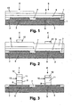
- Figs. 1 to 6 diagrammatically depict a cross section through a semiconductor device in successive stages of the fabrication with the aid of a first preferred embodiment of a method according to the invention.
- the starting point is a semiconductor body 1 having a substrate 2.
- the substrate 2 which in the embodiment under discussion is a p-type silicon substrate 2 but may in general be any other suitable substrate
- a first MOSFET transistor 4 will be formed at the location of an n-type semiconductor region 3 which has been introduced into the p-type substrate 2 (cf. Fig. 1 ).
- a part of the n-type semiconductor region 3 will then form the channel region 3A of this first MOSFET transistor 4.
- channel region 5 of a second MOSFET transistor 6 will be formed in an adjacent part of the substrate 2.
- the channel regions 3A, 5 of two adjacent transistors 4, 6 are electrically isolated from one another by means of insulating regions 7, which may, for example, be formed from silicon dioxide.
- insulating regions 7 are also known as field insulation regions, and in advanced technologies they may be formed by the etching of trenches into the substrate 2, which are then filled with an oxide. Therefore, these insulating regions 7 are also referred to as trench isolation.
- the surface of the semiconductor body 1 is covered with a dielectric layer 8 which, by way of example, may contain silicon dioxide but which may also be made from any suitable dielectric material, and which may have a thickness of between, for example, 0.5 and 1.5 nm.
- a metal layer 9 is applied to this dielectric layer 8.
- This metal layer 9 may, for example, comprise nickel, titanium or cobalt or a combination thereof and may have a thickness of between 5 and 50 nm. In the preferred embodiment described, the metal layer 9 contains nickel and has a thickness of 5 nm.
- the metal layer 9 can be deposited with the aid of, for example, a physical vapour deposition (PVD) technique, such as for example sputtering.
- PVD physical vapour deposition
- a mask 10 is deposited on this metal layer, for example with the aid of photolithography. This mask 10 may be made, for example, from photoresist.
- the metal layer 9 is removed at the location of the second transistor 6 which is to be formed, with the aid of the deposited mask 10.
- This step is illustrated in Fig. 2 .
- This can be done, for example, by means of etching with the aid of an etchant comprising sulphuric acid and hydrogen peroxide.
- the mask 10 is removed, for example with the aid of what is known as a mask stripper.
- a plasma etching process can be used for this purpose.
- a silicon layer 11 for example an n-type doped polycrystalline silicon, is applied with the aid of, for example, chemical vapour deposition (CVD) or physical vapour deposition, such as for example sputtering.
- CVD chemical vapour deposition
- PVD physical vapour deposition
- the thickness of the silicon layer 11 may, for example, be between 20 and 100 nm and in this embodiment is 50 nm.
- the silicon layer 11 may be relatively thick, with the result that the gate electrodes 13, 14 of the transistors 4, 6 which are to be formed may be of a suitable and approximately equal height.
- a mask 12 is patterned on the silicon layer 11 at the location of the gate electrodes 13, 14 which are to be formed for the two transistors 4, 6.
- the superfluous parts of the layer structure outside the masks 12 are removed, for example by etching, in the embodiment described by means of a dry plasma etching process.
- the semiconductor body 1 in this case functions as an etching stop layer.
- the remaining parts form the gate electrodes 13, 14 of the transistors 4, 6 which are to be formed (cf. Fig. 3 ).
- the mask 12 is removed, for example in the manner which has been described above for the removal of mask 10 (cf. Fig. 4 ).
- an insulating layer (not shown in the drawing) of, for example, silicon nitride is applied over the structure shown in Fig. 3 without the mask 12.
- the flat parts of this layer, located on the gate electrodes 13, 14 and between them, are then removed again, for example by means of an anisotropic plasma etching process. In this way, spacers 15 are formed against the side walls of the gate electrodes 13, 14 by the remaining parts of the silicon nitride layer.
- the source and drain regions 16, 17 and 18, 19 of the two transistors 4, 6, respectively, are formed by means of ion implantation.
- This step can be carried out, for example, by first of all forming source and drain regions 16, 17 of the first transistor 4, for example by means of a boron ion implantation step, with the second transistor 6 covered with a photoresist mask (not shown in the drawing). Then, in a similar way, source and drain region 18, 19 of the second transistor 6 are formed, for example using an arsenic ion implantation step.
- the transistors 4, 6 are also provided with what is known as LDD (lightly doped drain) regions (16A, 17A and 18A, 19A), which means that before the spacers 15 are formed, a lightly doped part of source and drain regions 16, 17 respectively 18, 19 of the transistors 4, 6, has already been formed.
- LDD lightly doped drain
- the metal layer 9 is converted, through interaction with the silicon layer 11 above it, into a disilicide region 20 at the location of the first transistor 4.
- the abovementioned temperature range is suitable not only for the formation of nickel disilicide but also for the formation of a metal disilicide in general (cf. US-6,440,851 Figs. 4a and b ).
- a further metal layer 21 is applied (cf. Fig. 5 ), which in this embodiment of the invention likewise contains nickel.
- the thickness of the further metal layer 21 is preferably between 5 and 50 nm.
- a part 22 of the further metal layer 21 is incorporated in the polycrystalline silicon 11 of the gate electrodes 13, 14 by means of a heat treatment, with the result that a metal silicide is formed.
- Similar parts 23 of the further metal layer 21 are in the process incorporated in the semiconductor body 1, likewise so as to form metal silicide, at the location of source and drain regions 16, 17 respectively 18, 19 of the two transistors 4, 6.
- the remaining part of the further metal layer 21 is removed by etching.
- a heat treatment lasting a few minutes at a second, lower temperature in a temperature range between, for example, 450°C and 650°C then in the silicon of the gate electrodes 13, 14 further metal silicide or, for the particular embodiment described here, nickel monosilicide regions 24, 25, are subsequently formed in the first gate electrode 13 and the second gate electrode 14, respectively.
- the temperature range given above is generally suitable for the formation of a monosilicide of a metal (cf. US 6,440,851 Figs. 4a and b ). Since the two temperature ranges, namely that used for the formation of disilicide and that used for the formation of monosilicide, are to be applicable to all possible silicide-forming metals, the two regions adjoin or may even overlap one another.
- the conditions for the formation of the further metal silicide are selected in such a manner that this further silicide in the second transistor is formed as far as the dielectric layer 8.
- the invention is in this context based on the insight that a metal disilicide generally has a different work function from a monosilicide.
- a region 24 having a higher work function namely that of the nickel disilicide, is located on top of/adjacent the dielectric layer 8 in transistor 4, and a nickel monosilicide having a lower work function is located in transistor 6.
- the silicide having the higher work function can be selected for the PMOST and the silicide having the lower work function can be selected for the NMOST.
- contact regions 26, 27 are also formed in the source and drain regions 16, 17 and 18, 19 of the two transistors 4, 6.
- the metal silicide it is preferable for the metal silicide to be formed as a silicon-rich silicide. This is thermodynamically the most stable with respect to silicon. A silicide of this type is often formed at elevated temperatures. Moreover, it generally has the lowest electrical resistance. If nickel is selected for the metal layer, the work function of the disilicide is closest to the value desired for a PMOST 4. The nickel monosilicide, having a lower work function, is more suitable for an NMOST 6 and can be formed at a lower temperature.
- metal silicide leads to the formation of a disilicide at higher temperatures while a monosilicide at lower temperatures, the two processes can as far as possible be carried out independently of one another, since the first process (formation of metal disilicide) cannot be carried out successfully at the temperature of the second process (formation of metal monosilicide).
- the first transistor 4 is formed as a PMOS transistor. If the metal silicide is formed as a nickel disilicide, in any event a silicide having the highest work function is located in the vicinity of the dielectric layer 4 in the first gate electrode 13, which is desirable for a PMOST.
- CMOS complementary metal-oxide-semiconductor
- insulators and a desired conductor pattern as well as connection regions are applied.
- Individual devices 30 are obtained by means of a separation technique, such as for example sawing.
- the method according to the invention is based on the insight that the etching of a layer other than the silicon layer 11, in this case the metal layer 9, makes it possible to provide one of the gate electrodes 13 with a metal silicide 24 that adjoins the dielectric layer 8 and has a first work function, while the other gate electrode 14 in the vicinity of the dielectric layer 8 may contain a material 25 having a different work function.
- the etching of a material other than the silicon layer 11, in particular of the metal layer 9 which has a lower thickness than the silicon layer 11, avoids asymmetry in the structure of the two transistors 4, 6.
- metal layer 9 can be removed particularly selectively with respect to the material of the dielectric layer 8 before the metal silicide is formed.
- the result is also a more symmetrical structure compared to the prior art, since the gate electrodes 13, 14 of the two transistors 4, 6 can still comprise silicon without an additional silicon deposition step being required for this purpose.
- the gate electrodes 13, 14 of the two transistors 4, 6 can be provided with very favourable properties, such as a low resistance and the absence of what is known as the depletion layer effect. This also offers the option of providing source and drain regions 16, 17 and 18, 19 of the two transistors 4, 6 with a connection conductor 26, 27 in the form of a silicide in a single process step.
- one significant advantage of a method according to the invention is that the use of the further metal silicide opens up the possibility of forming the two gate electrodes 13, 14 using metal silicides 24, 25 having a different silicon content. This also enables the two gate electrodes 13, 14 in the vicinity of the dielectric layer 8 to be provided with a silicide-containing part having a different composition which is suitable for PMOST and NMOST, respectively.
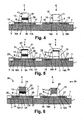
- Figs. 7 to 12 diagrammatically depict a cross section through a semiconductor device 40 in successive stages of the fabrication in accordance with a second embodiment of the method according to the invention.
- Figs. 7 to 12 diagrammatically depict a cross section through a semiconductor device 40 in successive stages of the fabrication in accordance with a second embodiment of the method according to the invention.
- the differences compared to the method described above will be explained.
- Corresponding or identical process steps can be carried out as discussed above in connection with the first embodiment.
- a dielectric layer 8 which in the present embodiment comprises silicon dioxide but which may be made from any suitable dielectric material and may, for example, be between 0.5 and 1.5 nm thick.
- This metal layer 31 consists of a metal which is stable compared to a metal layer which is subsequently to be applied and with which a metal silicide will be formed and also compared to the metal silicide which is to be formed.
- the metal layer 31 may, for example, be a layer of molybdenum, tungsten, platinum, iridium, tantalum, hafnium or any other suitable metal and can be deposited on the dielectric layer for example by means of vapour deposition. With the aid of a mask 32, metal layer 31 is removed at the location of the first transistor 4, for example by etching.
- a metal layer 9 is applied, for example by vapour deposition, followed by deposition of a polycrystalline silicon layer 11, for example by means of CVD. These layers 9 and 11 may have similar thicknesses to the layers 9 and 11 in the first embodiment.
- the metal layer 9 comprises nickel, but may also comprise other metals, such as for example cobalt or titanium.
- a mask 33 is patterned on the structure which has been formed (cf. Fig. 8 ).
- the gate electrodes 13, 14 of the two transistors 4, 6 are formed, for example by means of plasma etching with the aid of mask 33. This is illustrated in Fig. 9 .
- the mask 33 is removed and source and drain regions 16, 17 respectively 18, 19 of the two transistors 4, 6 are formed, as are spacers 15.
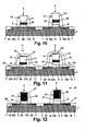
- the nickel layer 9 is converted into a nickel disilicide region 20, 35 in the first gate electrode 13 and second gate electrode 14, respectively ( Fig. 10 ).
- a further metal layer 21 is applied, which in this embodiment is nickel.
- a heat treatment at a second, lower temperature for example in a temperature range between 450°C and 650°C, once again causes parts 22 and 23 of the further metal layer 21 to be incorporated in the semiconductor body 1, respectively at the location of the gate electrodes 13, 14 and the source and drain regions 16, 17 and 18, 19 of the transistors 4, 6 ( Fig. 11 ).
- the remaining part of the further metal layer 21 has been removed by means of etching, for example, the remaining silicon parts of the gate electrodes 13, 14 are converted into nickel disilicide 34, 35 by means of a suitable heat treatment at a third, again higher temperature, for example in a temperature range between 650°C and 850°C ( Fig. 12 ).
- the first gate electrode 13 of the PMOST in the vicinity of the dielectric layer 8, includes a part 34 which comprises a disilicide with a relatively high work function, while inert metal, such as molybdenum 31, with a lower work function suitable for the NMOST is still present in the vicinity of the dielectric layer 8 in the other gate electrode 14 of the NMOST (second transistor 6).
- the treatment can be continued as has already been discussed above.
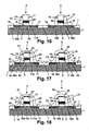
- Figs. 13 to 20 diagrammatically depict a cross section through a semiconductor device in successive stages of the fabrication in accordance with a third embodiment of the method according to the invention.
- the applied metal layer 9 which, by way of example, is a nickel layer ( Fig. 13 )
- a gate electrode mask 41 is applied for the purpose of forming the gate electrodes 13, 14 (cf. Fig. 14 ).
- spacers 15 are formed (cf. Fig. 16 ) and regions 20, 34 of metal disilicide, for example a disilicide of nickel, are formed by a suitable heat treatment at a first, high temperature, for example in a temperature range between 650°C and 850°C.
- silicided regions 22 and 23 of monosilicide are formed as described in the previous embodiments by the use of a suitable heat treatment at a second, lower temperature in a temperature range between 450°C and 650°C.
- a mask 42 is formed on the second gate electrode 14 at the location of the second transistor 6.
- the metal layer 21 is removed in regions where it is not covered by mask 42, with a part of this layer located on top of the second gate electrode 14 remaining in place.
- the silicon parts of the gate electrodes 13, 14 are converted into nickel monosilicide regions 24, 25 by means of a heat treatment at the second, lower temperature in the temperature range between 450°C and 650°C.
- the excess of nickel that is present at the location of the second gate electrode 14 also converts the nickel disilicide 35 which is present therein into nickel monosilicide 25 ( Fig. 20 ).
- the two transistors 4, 6 with a part 20, 25 which is located in the vicinity of the dielectric layer 8 and has a different work function suitable for the corresponding transistor (cf. above).
- the further metal layer 21 is preferably applied after the formed layers have been removed all the way down to the surface of the semiconductor body 1 outside the regions of the first and second gate electrodes 13, 14, and that the further metal layer 21 is also used for the contact-connection of the source and drain regions 16, 17 and 18, 19 of the two transistors 4, 6.
- This makes it easy to fabricate both NMOS and PMOS transistors with different work functions, with a low resistance in the gate electrodes 13, 14 and in the contact regions 26, 27 of the source and drain regions 16, 17 and 18, 19 and without the undesirable so-called depletion layer effect.
- the invention is not restricted to the exemplary embodiments described, since numerous variations and modifications will be possible within the scope of the invention for the person skilled in the art. For example, it is possible to produce devices having a different geometry and/or different dimensions.
- Si substrate it is also possible to use a glass, ceramic or plastic substrate.
- the semiconductor body can then be formed by what is known as the SOI (Silicon on Insulator). In this context, it is optionally possible to use what is known as a substrate transfer technique.
- materials other than those mentioned in the examples can be used within the scope of the invention.
- other metals such as cobalt, instead of nickel.
- other deposition techniques for the above-mentioned or other materials, such as epitaxy, sputtering and vapour deposition.
- dry techniques such as plasma etching, to be used instead of wet-chemical etching methods, and vice versa.
- the dielectric layer 8 for the two transistors 4, 6 it is not necessary for the dielectric layer 8 for the two transistors 4, 6 to be made from the same material or to be of the same thickness.
- the device may include further active and passive semiconductor elements or electronic components, such as a greater number of diodes and/or transistors and resistors and/or capacitors, optionally in the form of an integrated circuit. Obviously, the fabrication is then adapted appropriately.
Landscapes
- Electrodes Of Semiconductors (AREA)
- Thin Film Transistor (AREA)
- Metal-Oxide And Bipolar Metal-Oxide Semiconductor Integrated Circuits (AREA)
Abstract
Description
- The present invention relates to a method for fabricating semiconductor devices having a dielectric layer and at least two silicided electrodes, that part of each of the at least two silicided electrodes which adjoins the dielectric layer having a different work function.
- The fabrication of, for example, silicon CMOSFETs (complementary metal oxide semiconductor field-effect transistors) requires PMOS and NMOS structures or transistors on the same substrate. In this context, for both types of transistors to operate optimally, it is important for the work function of at least that part of the gate electrode of the first transistor, for example a PMOST, which adjoins the dielectric layer to differ from that of the second, for example an NMOST. The latter requires a gate electrode with a low work function, namely a work function which is in the vicinity of that of n-type polycrystalline silicon, i.e. approximately 4.2 eV, whereas the former needs a work function which is in the vicinity of that of p-type polycrystalline silicon, i.e. 5.2 eV.
- A method for fabricating structures of this type is known from
EP 1211729 . That document shows the fabrication of a couple of MOS transistors, wherein a metal layer is to be applied to a dielectric layer located in the regions of both transistors, and then a silicon layer is to be applied to the metal layer. The silicon layer is removed again at the location of one of the two transistors with the aid of photolithography and etching, after which, with the aid of a heat step, the silicon at the location of the other transistor is brought into reaction with the metal beneath it, forming a metal silicide which then adjoins the dielectric layer. The gate electrode of the first transistor formed next to the latter then contains a metal adjoining the dielectric layer. In this way, inEP 1211729 , adjacent gate electrodes with different work functions are formed, the specific work functions being that of the silicide and that of the metal, and consequently both NMOS and PMOS transistors can be simultaneously provided with optimum properties. - One drawback of the method discussed above is that the local removal of the silicon results in an undesired asymmetry in the structure of the two transistors, which has various associated drawbacks. The local removal of the silicon produces a difference in the thickness of the gate electrodes having a different work function. This difference in height can give rise to deviations in the width of the gate electrodes during the exposure step in which the pattern of the gate electrodes is formed in a photosensitive layer on top of the gate electrode layer. As a result, the electrical characteristics of the transistors may deviate from the desired value. This difference in thickness also makes it more difficult to form the spacers, since the dimensions of the latter are also determined by the height of the gate electrode against which these spacers bear. During the formation of the source and drain regions by means of an ion implantation step, this difference in thickness presents the risk of ions being implanted or being able to diffuse through the thinner gate electrode into the channel region below. To solve this problem, the implantation parameters have to be additionally optimized.
-
US-2002/0086491 describes a semiconductor device located on a semiconductor substrate having opposite types of first and second transistors formed thereon. The opposite types of first and second transistors are obtained by forming stacked gate electrodes having different gate layers over devices of a first type, and non-stacked gate electrodes over devices of another type. -
US-2003/0143825 discloses a semiconductor device comprising an n-type MIS transistor comprising a first gate insulating film and a first gate electrode including an MSix film formed on the first gate insulating film, and a p-type MIS transistor comprising a second gate insulating film and a second gate electrode including an MSiy film formed on the second gate insulating film. The different Msi films are formed by providing a Si film on top of a W film for both transistor types, then selectively removing the Si film in the p-type transistor and silicidising the W film for the n-type transistor. Thereafter a W film is deposited both on the p-type and on the n-type transistor. The result is a p-type transistor with a gate electrode structure comprising two layers of tungsten film, and an n-type transistor with a gate electrode structure comprising a tungsten film on top of a tungsten silicide film. -
EP-1328017 describes a method of forming first and second transistors with differing work function gates by different metals deposited to react with silicon. A layer of first metal is deposited on a silicon-coated substrate. The first metal is selectively removed from a first region. The remaining first metal is then caused to react with the silicon, to form a first metal-silicide over a second region. A second metal is then provided, and caused to react with the silicon at the first region, thus forming a second metal-silicide over the first region. - It is an object of the present invention to provide a method which makes it easy to form two electrodes having a different work function, in particular a method in which both a NMOS transistor and a PMOS transistor can be fabricated simultaneously with gate electrodes whose parts that adjoin the dielectric layer have a different and appropriate work function and which does not have the abovementioned drawback of asymmetry.
- There is disclosed a method for fabricating a semiconductor device as recited in
claim 1. - A first embodiment of the invention provides a method for fabricating a semiconductor device having a semiconductor body, the semiconductor body comprising:
- a first semiconductor structure having a dielectric layer and a first electrode that comprises a first conductor, and
- a second semiconductor structure having a dielectric layer and a second electrode that comprises a second conductor which differs from the first conductor and of which the part that adjoins the dielectric layer has a different work function from the corresponding part of the first conductor.
- In the method of the invention, after the dielectric layer has been applied to the semiconductor body, a first metal layer is applied to the dielectric layer, and then a silicon layer is applied to the first metal layer and these two layers are brought into reaction with one another at the location of at least one semiconductor structure, with a first metal silicide being formed. The method according to the invention is characterized in that the parts of the conductors having different work functions are formed by etching a layer other than the silicon layer at the location of one of the two semiconductor structures.
- One specific exemplary embodiment of the invention describes a method for fabricating a semiconductor device having a substrate and a semiconductor body, wherein the semiconductor body may comprise:
- a first field-effect transistor comprising a first source and drain region and having a channel region of a first conduction type and comprising a first gate electrode which is separated from the channel region by a dielectric layer and comprises a first conductor, and
- a second field-effect transistor comprising a second source and drain region and comprising a channel region of a second conduction type, which is the opposite conduction type from the first conduction type, and comprising a second gate electrode, which is separated from the channel region by a dielectric layer and comprises a second conductor which differs from the first conductor and of which the part that adjoins the dielectric layer has a different work function from the corresponding part of the first conductor.
- In a preferred embodiment of the invention, the first metal layer may be a siliciding metal layer. This layer may be formed at the location of both semiconductor structures and may, prior to the deposition of the silicon layer, be removed at the location of, for example, the second transistor, for example by etching. This first metal layer may be very thin and is preferably between 5 and 50 nm thick and may contain various suitable metals which form a silicide with silicon, such as for example nickel, titanium or cobalt, and in a preferred embodiment is nickel.
- In another embodiment, a second, non-siliciding metal layer is arranged between the first metal layer and the dielectric layer. In this case, the first metal layer, which is a siliciding metal layer, can be deposited on top of the second metal layer. The non-siliciding metal layer may, for example, be a layer of molybdenum, tungsten, platinum, iridium, tantalum, hafnium or another suitable metal. This non-siliciding metal layer preferably comprises a metal which is stable compared to the metal of the first metal layer and compared to the metal silicide which is to be formed. Metals such as tungsten, molybdenum and tantalum are particularly suitable with regard to the desired stability compared to a metal which forms a metal silicide and the silicide which is thereby formed. In this embodiment of the invention, the second metal layer, i.e. the non-siliciding metal layer, is removed, for example by etching, at the location of one of the transistors. This removal can be effected prior to the deposition of the silicon layer.
- The method may also include the deposition of a third metal layer after the first and second semiconductor structures have been formed, wherein the third metal layer is a siliciding metal layer, which for example may comprise nickel, titanium or cobalt, and with which a further metal silicide can be formed at the location of at least one semiconductor structure. The further metal silicide may have a different silicon content from the first metal silicide. In one embodiment of the invention, the first metal silicide may be formed as a disilicide, and the further metal silicide may be formed as a monosilicide.
- In a further embodiment of the invention, the etching of a layer other than the silicon layer can be implemented as the removal of a part of the first, second or third metal layer. The first or second metal layer can be etched prior to the application of the silicon layer.
- In one specific example of the invention, the first semiconductor structure and the second semiconductor structure may be a field-effect transistor having a source and drain region and a gate electrode. In this example, the third metal layer can be used for the contact-connection of source and drain region.
- Other characteristics, properties and advantages of the present invention will become clear from the following detailed description in conjunction with the appended figures which, as an example, illustrate the basic principles of the invention.
-
-
Figs. 1 to 6 diagrammatically depict a cross section through a semiconductor device in successive stages of the fabrication in accordance with a first embodiment of a method according to the invention; -
Figs. 7 to 12 diagrammatically depict a cross section through a semiconductor device in successive stages of the fabrication in accordance with a second embodiment of a method according to the invention; -
Figs. 13 to 20 diagrammatically depict a cross section through a semiconductor device in successive stages of the fabrication in accordance with a third embodiment of a method according to the invention. - The present invention will be described below with the aid of various embodiments and with reference to various figures. However, the invention is not restricted to these embodiments and figures. The figures described are only diagrammatic and also do not restrict the invention. The dimensions of some elements may be exaggerated and not to scale in the figures in order to explain a particular concept.
- The method of the present invention can be used to fabricate semiconductor structures having two electrodes with different work functions. In one particular case, for example, it is possible to fabricate semiconductor structures which are provided with a control electrode, such as for example a gate electrode, and a first and second main electrode, such as for example a source and drain region. The following text will discuss the fabrication of a semiconductor device having two semiconductor structures, each with a gate electrode and a source and drain region in accordance with the present invention. However, this is done only in the context of discussion of the invention and does not impose any restriction on the invention.
-
Figs. 1 to 6 diagrammatically depict a cross section through a semiconductor device in successive stages of the fabrication with the aid of a first preferred embodiment of a method according to the invention. During formation of thedevice 30, the starting point is asemiconductor body 1 having asubstrate 2. In thesubstrate 2, which in the embodiment under discussion is a p-type silicon substrate 2 but may in general be any other suitable substrate, during the subsequent stages afirst MOSFET transistor 4 will be formed at the location of an n-type semiconductor region 3 which has been introduced into the p-type substrate 2 (cf.Fig. 1 ). A part of the n-type semiconductor region 3 will then form thechannel region 3A of thisfirst MOSFET transistor 4. Then,channel region 5 of asecond MOSFET transistor 6 will be formed in an adjacent part of thesubstrate 2. Thechannel regions adjacent transistors regions 7, which may, for example, be formed from silicon dioxide. These insulatingregions 7 are also known as field insulation regions, and in advanced technologies they may be formed by the etching of trenches into thesubstrate 2, which are then filled with an oxide. Therefore, these insulatingregions 7 are also referred to as trench isolation. - The surface of the
semiconductor body 1 is covered with adielectric layer 8 which, by way of example, may contain silicon dioxide but which may also be made from any suitable dielectric material, and which may have a thickness of between, for example, 0.5 and 1.5 nm. Then, ametal layer 9 is applied to thisdielectric layer 8. Thismetal layer 9 may, for example, comprise nickel, titanium or cobalt or a combination thereof and may have a thickness of between 5 and 50 nm. In the preferred embodiment described, themetal layer 9 contains nickel and has a thickness of 5 nm. Themetal layer 9 can be deposited with the aid of, for example, a physical vapour deposition (PVD) technique, such as for example sputtering. Then, amask 10 is deposited on this metal layer, for example with the aid of photolithography. Thismask 10 may be made, for example, from photoresist. - In a subsequent step, the
metal layer 9 is removed at the location of thesecond transistor 6 which is to be formed, with the aid of the depositedmask 10. This step is illustrated inFig. 2 . This can be done, for example, by means of etching with the aid of an etchant comprising sulphuric acid and hydrogen peroxide. Then, themask 10 is removed, for example with the aid of what is known as a mask stripper. By way of example, a plasma etching process can be used for this purpose. Then, after cleaning, asilicon layer 11, for example an n-type doped polycrystalline silicon, is applied with the aid of, for example, chemical vapour deposition (CVD) or physical vapour deposition, such as for example sputtering. The thickness of thesilicon layer 11 may, for example, be between 20 and 100 nm and in this embodiment is 50 nm. Thesilicon layer 11 may be relatively thick, with the result that thegate electrodes transistors mask 12 is patterned on thesilicon layer 11 at the location of thegate electrodes transistors - After that, the superfluous parts of the layer structure outside the
masks 12 are removed, for example by etching, in the embodiment described by means of a dry plasma etching process. Thesemiconductor body 1 in this case functions as an etching stop layer. The remaining parts form thegate electrodes transistors Fig. 3 ). - In a subsequent step, the
mask 12 is removed, for example in the manner which has been described above for the removal of mask 10 (cf.Fig. 4 ). Then, for example with the aid of CVD, an insulating layer (not shown in the drawing) of, for example, silicon nitride is applied over the structure shown inFig. 3 without themask 12. The flat parts of this layer, located on thegate electrodes gate electrodes - Next, the source and drain
regions transistors regions first transistor 4, for example by means of a boron ion implantation step, with thesecond transistor 6 covered with a photoresist mask (not shown in the drawing). Then, in a similar way, source and drainregion second transistor 6 are formed, for example using an arsenic ion implantation step. In this embodiment of the invention, thetransistors spacers 15 are formed, a lightly doped part of source and drainregions transistors metal layer 9 is converted, through interaction with thesilicon layer 11 above it, into adisilicide region 20 at the location of thefirst transistor 4. The abovementioned temperature range is suitable not only for the formation of nickel disilicide but also for the formation of a metal disilicide in general (cf.US-6,440,851 Figs. 4a and b ). - Then, a
further metal layer 21 is applied (cf.Fig. 5 ), which in this embodiment of the invention likewise contains nickel. The thickness of thefurther metal layer 21 is preferably between 5 and 50 nm. Then, in this embodiment, apart 22 of thefurther metal layer 21 is incorporated in thepolycrystalline silicon 11 of thegate electrodes Similar parts 23 of thefurther metal layer 21 are in the process incorporated in thesemiconductor body 1, likewise so as to form metal silicide, at the location of source and drainregions transistors - Then, the remaining part of the
further metal layer 21 is removed by etching. During a heat treatment lasting a few minutes at a second, lower temperature in a temperature range between, for example, 450°C and 650°C, then in the silicon of thegate electrodes nickel monosilicide regions first gate electrode 13 and thesecond gate electrode 14, respectively. The temperature range given above is generally suitable for the formation of a monosilicide of a metal (cf.US 6,440,851 Figs. 4a and b ). Since the two temperature ranges, namely that used for the formation of disilicide and that used for the formation of monosilicide, are to be applicable to all possible silicide-forming metals, the two regions adjoin or may even overlap one another. - It is preferable for the conditions for the formation of the further metal silicide to be selected in such a manner that this further silicide in the second transistor is formed as far as the
dielectric layer 8. The invention is in this context based on the insight that a metal disilicide generally has a different work function from a monosilicide. In the preferred embodiment, therefore, aregion 24 having a higher work function, namely that of the nickel disilicide, is located on top of/adjacent thedielectric layer 8 intransistor 4, and a nickel monosilicide having a lower work function is located intransistor 6. By way of example, the silicide having the higher work function can be selected for the PMOST and the silicide having the lower work function can be selected for the NMOST. Furthermore,contact regions regions transistors - It is preferable for the metal silicide to be formed as a silicon-rich silicide. This is thermodynamically the most stable with respect to silicon. A silicide of this type is often formed at elevated temperatures. Moreover, it generally has the lowest electrical resistance. If nickel is selected for the metal layer, the work function of the disilicide is closest to the value desired for a
PMOST 4. The nickel monosilicide, having a lower work function, is more suitable for anNMOST 6 and can be formed at a lower temperature. Since the formation of metal silicide leads to the formation of a disilicide at higher temperatures while a monosilicide at lower temperatures, the two processes can as far as possible be carried out independently of one another, since the first process (formation of metal disilicide) cannot be carried out successfully at the temperature of the second process (formation of metal monosilicide). - It is preferable for the
first transistor 4 to be formed as a PMOS transistor. If the metal silicide is formed as a nickel disilicide, in any event a silicide having the highest work function is located in the vicinity of thedielectric layer 4 in thefirst gate electrode 13, which is desirable for a PMOST. - The fabrication of the semiconductor device using the method of the present invention is then continued in the way which is customary in CMOS technology. In particular further insulators and a desired conductor pattern as well as connection regions are applied.
Individual devices 30 are obtained by means of a separation technique, such as for example sawing. - The method according to the invention is based on the insight that the etching of a layer other than the
silicon layer 11, in this case themetal layer 9, makes it possible to provide one of thegate electrodes 13 with ametal silicide 24 that adjoins thedielectric layer 8 and has a first work function, while theother gate electrode 14 in the vicinity of thedielectric layer 8 may contain amaterial 25 having a different work function. The etching of a material other than thesilicon layer 11, in particular of themetal layer 9 which has a lower thickness than thesilicon layer 11, avoids asymmetry in the structure of the twotransistors - At the location of the
second transistor 6,metal layer 9 can be removed particularly selectively with respect to the material of thedielectric layer 8 before the metal silicide is formed. The result is also a more symmetrical structure compared to the prior art, since thegate electrodes transistors further metal layer 21 to thesilicon layer 7 at the location of the twotransistors gate electrodes transistors regions transistors connection conductor - Finally, one significant advantage of a method according to the invention is that the use of the further metal silicide opens up the possibility of forming the two
gate electrodes metal silicides gate electrodes dielectric layer 8 to be provided with a silicide-containing part having a different composition which is suitable for PMOST and NMOST, respectively. -
Figs. 7 to 12 diagrammatically depict a cross section through asemiconductor device 40 in successive stages of the fabrication in accordance with a second embodiment of the method according to the invention. In discussing these figures, in particular the differences compared to the method described above will be explained. Corresponding or identical process steps can be carried out as discussed above in connection with the first embodiment. - The surface of a
semiconductor body 1 is covered with adielectric layer 8, which in the present embodiment comprises silicon dioxide but which may be made from any suitable dielectric material and may, for example, be between 0.5 and 1.5 nm thick. Ametal layer 31, which may preferably be from 5 to 50 nm thick and in the present embodiment is 10 nm thick, is applied on top of the dielectric layer 8 (Fig. 7 ). Thismetal layer 31 consists of a metal which is stable compared to a metal layer which is subsequently to be applied and with which a metal silicide will be formed and also compared to the metal silicide which is to be formed. Themetal layer 31 may, for example, be a layer of molybdenum, tungsten, platinum, iridium, tantalum, hafnium or any other suitable metal and can be deposited on the dielectric layer for example by means of vapour deposition. With the aid of amask 32,metal layer 31 is removed at the location of thefirst transistor 4, for example by etching. - After the
mask 32 has been removed, ametal layer 9 is applied, for example by vapour deposition, followed by deposition of apolycrystalline silicon layer 11, for example by means of CVD. Theselayers layers metal layer 9 comprises nickel, but may also comprise other metals, such as for example cobalt or titanium. Then, amask 33 is patterned on the structure which has been formed (cf.Fig. 8 ). - Then, the
gate electrodes transistors mask 33. This is illustrated inFig. 9 . Next, themask 33 is removed and source and drainregions transistors - During a suitable heat treatment at a first, high temperature, for example in a temperature range between 650°C and 850°C, the
nickel layer 9 is converted into anickel disilicide region first gate electrode 13 andsecond gate electrode 14, respectively (Fig. 10 ). - Then, a
further metal layer 21 is applied, which in this embodiment is nickel. A heat treatment at a second, lower temperature, for example in a temperature range between 450°C and 650°C, once again causesparts further metal layer 21 to be incorporated in thesemiconductor body 1, respectively at the location of thegate electrodes regions transistors 4, 6 (Fig. 11 ). After the remaining part of thefurther metal layer 21 has been removed by means of etching, for example, the remaining silicon parts of thegate electrodes nickel disilicide Fig. 12 ). Therefore, thefirst gate electrode 13 of the PMOST (first transistor 4), in the vicinity of thedielectric layer 8, includes apart 34 which comprises a disilicide with a relatively high work function, while inert metal, such asmolybdenum 31, with a lower work function suitable for the NMOST is still present in the vicinity of thedielectric layer 8 in theother gate electrode 14 of the NMOST (second transistor 6). The treatment can be continued as has already been discussed above. - Therefore, with the aid of this second embodiment of the invention, it is once again possible to form a
first transistor 4 and asecond transistor 6 whose regions adjoining thedielectric layer 8 have different work functions. -
Figs. 13 to 20 diagrammatically depict a cross section through a semiconductor device in successive stages of the fabrication in accordance with a third embodiment of the method according to the invention. In particular the differences from the methods discussed above will be explained in the discussion of these figures. Corresponding or identical process steps can be carried out as discussed in connection with the first or second embodiment. In this third embodiment, the appliedmetal layer 9, which, by way of example, is a nickel layer (Fig. 13 ), is not locally removed, but rather is completely covered with asilicon layer 11, after which agate electrode mask 41 is applied for the purpose of forming thegate electrodes 13, 14 (cf.Fig. 14 ). After thegate electrodes Fig. 15 ), spacers 15 are formed (cf.Fig. 16 ) andregions - After
further metal layer 21, for example a nickel layer, has been applied (cf.Fig. 17 ),silicided regions Fig. 18 ), amask 42 is formed on thesecond gate electrode 14 at the location of thesecond transistor 6. Next (cf.Fig. 19 ) themetal layer 21 is removed in regions where it is not covered bymask 42, with a part of this layer located on top of thesecond gate electrode 14 remaining in place. Then, the silicon parts of thegate electrodes nickel monosilicide regions second gate electrode 14 also converts thenickel disilicide 35 which is present therein into nickel monosilicide 25 (Fig. 20 ). In this way it is once again possible to provide the twotransistors part dielectric layer 8 and has a different work function suitable for the corresponding transistor (cf. above). - It should be noted that in all cases the
further metal layer 21 is preferably applied after the formed layers have been removed all the way down to the surface of thesemiconductor body 1 outside the regions of the first andsecond gate electrodes further metal layer 21 is also used for the contact-connection of the source and drainregions transistors gate electrodes contact regions regions - The invention is not restricted to the exemplary embodiments described, since numerous variations and modifications will be possible within the scope of the invention for the person skilled in the art. For example, it is possible to produce devices having a different geometry and/or different dimensions. As an alternative to an Si substrate, it is also possible to use a glass, ceramic or plastic substrate. The semiconductor body can then be formed by what is known as the SOI (Silicon on Insulator). In this context, it is optionally possible to use what is known as a substrate transfer technique.
- It should also be noted that materials other than those mentioned in the examples can be used within the scope of the invention. For example, it is also possible to use other metals, such as cobalt, instead of nickel. It should be expressly noted that where the examples opt to use the same metal for the
metal layer 9 and thefurther metal layer 21, it is also possible to use different metals for the two layers. It is also possible to use other deposition techniques for the above-mentioned or other materials, such as epitaxy, sputtering and vapour deposition. It is also possible for "dry" techniques, such as plasma etching, to be used instead of wet-chemical etching methods, and vice versa. - It should also be noted that it is not necessary for the
dielectric layer 8 for the twotransistors - Furthermore, it should be noted that the device may include further active and passive semiconductor elements or electronic components, such as a greater number of diodes and/or transistors and resistors and/or capacitors, optionally in the form of an integrated circuit. Obviously, the fabrication is then adapted appropriately.
Claims (12)
- Method for fabricating a semiconductor device having a semiconductor body (1), the semiconductor body (1) comprising:- a first semiconductor structure (4) having a dielectric layer (8) and a first electrode (13) that comprises a first conductor, and- a second semiconductor structure (6) having a dielectric layer (8) and a second electrode (14) that comprises a second conductor which differs from the first conductor and of which the part (25) that adjoins the dielectric layer (8) has a different work function from the corresponding part (20) of the first conductor,wherein after the dielectric layer (8) has been applied to the semiconductor body (1), a first metal layer (9) is applied onto the dielectric layer (8), and then a silicon layer (11) is applied to the metal layer and these two layers are reacted with one another at the location of at least one semiconductor structure (4, 6), with a first metal silicide being formed at that location, characterized in that the parts (20, 25) of the conductors having different work functions are formed by etching a layer other than the silicon layer (11) at the location of one of the two semiconductor structures (4, 6).
- Method according to claim 1, wherein the first metal layer consists of a metal selected from nickel, titanium or cobalt.
- Method according to one of the preceding claims, also comprising the application of a second metal layer (31) between the first metal layer (9) and the dielectric layer (8), the second metal layer being a non-siliciding metal layer.
- Method according to claim 3, wherein the second metal layer consists of a metal selected from molybdenum, tungsten, platinum, iridium, tantalum or hafnium.
- Method according to one of the preceding claims, wherein, after the first and second semiconductor structures (4, 6) have been formed, the method also comprises the deposition of a third metal layer (21), the third metal layer (21) being a siliciding metal layer, by means of which a further metal silicide is formed at the location of at least one of the first and second semiconductor structures (4, 6).
- Method according to claim 5, wherein the third metal layer (21) consists of a metal selected from nickel, titanium or cobalt.
- Method according to one of Claims 5 or 6, wherein the further metal silicide is formed with a silicon content different from the silicon content of the first metal silicide.
- Method according to claim 7, wherein the first metal silicide is formed as a disilicide and the further metal silicide is formed as a monosilicide.
- Method according to one of the preceding claims, wherein etching of a layer other than the silicon layer (11) is carried out by etching the first, second or third metal layer.
- Method according to claim 9, wherein the first or second metal layer is etched before the silicon layer (11) is applied.
- Method according to one of the preceding claims, wherein the first semiconductor structure (4) and second semiconductor structure (6) is a field-effect transistor having a gate electrode (13; 14) and a source and drain region (16, 17; 18, 19).
- Method according to claim 11, wherein the third metal layer (21) is used for the contact-connection of source and drain region (16, 17; 18, 19).
Applications Claiming Priority (2)
| Application Number | Priority Date | Filing Date | Title |
|---|---|---|---|
| BE2003/0548A BE1015723A4 (en) | 2003-10-17 | 2003-10-17 | METHOD FOR MANUFACTURING OF SEMICONDUCTOR DEVICES WITH silicided electrodes. |
| BE200300548 | 2003-10-17 |
Publications (2)
| Publication Number | Publication Date |
|---|---|
| EP1524688A1 EP1524688A1 (en) | 2005-04-20 |
| EP1524688B1 true EP1524688B1 (en) | 2009-12-09 |
Family
ID=34318708
Family Applications (1)
| Application Number | Title | Priority Date | Filing Date |
|---|---|---|---|
| EP04077816A Expired - Lifetime EP1524688B1 (en) | 2003-10-17 | 2004-10-13 | Method for fabricating semiconductor devices having silicided electrodes |
Country Status (8)
| Country | Link |
|---|---|
| US (2) | US7226827B2 (en) |
| EP (1) | EP1524688B1 (en) |
| JP (1) | JP4994585B2 (en) |
| CN (1) | CN1627502A (en) |
| AT (1) | ATE451718T1 (en) |
| BE (1) | BE1015723A4 (en) |
| DE (1) | DE602004024490D1 (en) |
| TW (1) | TWI242263B (en) |
Families Citing this family (28)
| Publication number | Priority date | Publication date | Assignee | Title |
|---|---|---|---|---|
| JP5015446B2 (en) * | 2005-05-16 | 2012-08-29 | アイメック | Method for forming double fully silicided gates and device obtained by said method |
| JP2007019395A (en) * | 2005-07-11 | 2007-01-25 | Renesas Technology Corp | Semiconductor device having mos structure and method for manufacturing the same |
| JP2007019400A (en) * | 2005-07-11 | 2007-01-25 | Renesas Technology Corp | Semiconductor device having mos structure and manufacturing method thereof |
| JP4784734B2 (en) * | 2005-09-12 | 2011-10-05 | 日本電気株式会社 | Semiconductor device and manufacturing method thereof |
| JP2009509324A (en) * | 2005-09-15 | 2009-03-05 | エヌエックスピー ビー ヴィ | Semiconductor device and manufacturing method thereof |
| JP2009509325A (en) * | 2005-09-15 | 2009-03-05 | エヌエックスピー ビー ヴィ | Semiconductor device and manufacturing method thereof |
| JP2007123548A (en) * | 2005-10-28 | 2007-05-17 | Renesas Technology Corp | Manufacturing method of semiconductor device |
| JP2009516910A (en) * | 2005-11-21 | 2009-04-23 | フリースケール セミコンダクター インコーポレイテッド | Method for forming a semiconductor device having a salicide layer |
| US20090045469A1 (en) * | 2005-11-28 | 2009-02-19 | Kensuke Takahashi | Semiconductor Device and Manufacturing Method Thereof |
| JP2007158065A (en) | 2005-12-06 | 2007-06-21 | Nec Electronics Corp | Semiconductor device manufacturing method and semiconductor device |
| JP4755894B2 (en) * | 2005-12-16 | 2011-08-24 | 株式会社東芝 | Semiconductor device and manufacturing method thereof |
| JP2007214436A (en) * | 2006-02-10 | 2007-08-23 | Tokyo Electron Ltd | Semiconductor device manufacturing method and semiconductor device |
| KR100729366B1 (en) * | 2006-05-19 | 2007-06-15 | 삼성전자주식회사 | Semiconductor Device and Forming Method |
| JP5280843B2 (en) * | 2006-05-25 | 2013-09-04 | ルネサスエレクトロニクス株式会社 | Method for forming metal compound layer and apparatus for forming metal compound layer |
| JP4920310B2 (en) * | 2006-05-30 | 2012-04-18 | 株式会社東芝 | Semiconductor device and manufacturing method thereof |
| JP2007324230A (en) * | 2006-05-30 | 2007-12-13 | Toshiba Corp | Semiconductor device and manufacturing method of semiconductor device |
| JP2008016538A (en) * | 2006-07-04 | 2008-01-24 | Renesas Technology Corp | Semiconductor device having MOS structure and manufacturing method thereof |
| WO2008013125A1 (en) * | 2006-07-25 | 2008-01-31 | Nec Corporation | Semiconductor device and method for manufacturing same |
| CN101523593B (en) * | 2006-09-29 | 2012-05-23 | 瑞萨电子株式会社 | Semiconductor device manufacturing method and semiconductor device |
| EP1928021A1 (en) * | 2006-11-29 | 2008-06-04 | Interuniversitair Microelektronica Centrum (IMEC) | Method of manufacturing a semiconductor device with dual fully silicided gate |
| JP2009027083A (en) | 2007-07-23 | 2009-02-05 | Toshiba Corp | Semiconductor device and manufacturing method thereof |
| JP2009044051A (en) * | 2007-08-10 | 2009-02-26 | Panasonic Corp | Semiconductor device and manufacturing method thereof |
| US20090053883A1 (en) * | 2007-08-24 | 2009-02-26 | Texas Instruments Incorporated | Method of setting a work function of a fully silicided semiconductor device, and related device |
| WO2009133509A1 (en) * | 2008-04-29 | 2009-11-05 | Nxp B.V. | Integrated circuit manufacturing method and integrated circuit |
| US8304841B2 (en) * | 2009-09-14 | 2012-11-06 | Taiwan Semiconductor Manufacturing Company, Ltd. | Metal gate transistor, integrated circuits, systems, and fabrication methods thereof |
| TWI550828B (en) * | 2011-06-10 | 2016-09-21 | 住友化學股份有限公司 | Semiconductor device, semiconductor substrate, method of manufacturing semiconductor substrate, and method of manufacturing semiconductor device |
| CN103137475B (en) * | 2011-11-23 | 2015-09-16 | 中国科学院微电子研究所 | A kind of semiconductor structure and its manufacturing method |
| CN104952734B (en) * | 2015-07-16 | 2020-01-24 | 矽力杰半导体技术(杭州)有限公司 | Semiconductor structure and manufacturing method thereof |
Citations (1)
| Publication number | Priority date | Publication date | Assignee | Title |
|---|---|---|---|---|
| EP1328017A2 (en) * | 2001-11-30 | 2003-07-16 | Texas Instruments Incorporated | Complementary Tranistors |
Family Cites Families (14)
| Publication number | Priority date | Publication date | Assignee | Title |
|---|---|---|---|---|
| US6087225A (en) * | 1998-02-05 | 2000-07-11 | International Business Machines Corporation | Method for dual gate oxide dual workfunction CMOS |
| JPH11260934A (en) * | 1998-03-10 | 1999-09-24 | Matsushita Electric Ind Co Ltd | Semiconductor device and manufacturing method thereof |
| JP2000223588A (en) * | 1999-02-03 | 2000-08-11 | Nec Corp | Complementary mis-type semiconductor device and its manufacture |
| US6200834B1 (en) * | 1999-07-22 | 2001-03-13 | International Business Machines Corporation | Process for fabricating two different gate dielectric thicknesses using a polysilicon mask and chemical mechanical polishing (CMP) planarization |
| US6187617B1 (en) * | 1999-07-29 | 2001-02-13 | International Business Machines Corporation | Semiconductor structure having heterogeneous silicide regions and method for forming same |
| US6440851B1 (en) | 1999-10-12 | 2002-08-27 | International Business Machines Corporation | Method and structure for controlling the interface roughness of cobalt disilicide |
| JP2001196467A (en) * | 1999-11-01 | 2001-07-19 | Hitachi Ltd | Semiconductor integrated circuit device and method of manufacturing the same |
| US6383879B1 (en) * | 1999-12-03 | 2002-05-07 | Agere Systems Guardian Corp. | Semiconductor device having a metal gate with a work function compatible with a semiconductor device |
| JP2002217313A (en) * | 2000-11-30 | 2002-08-02 | Texas Instruments Inc | Complementary transistors having respective gates formed from metal and corresponding metal silicide |
| US20020102802A1 (en) * | 2001-02-01 | 2002-08-01 | Tan Cheng Cheh | Novel technique to achieve thick silicide film for ultra-shallow junctions |
| JP3974507B2 (en) * | 2001-12-27 | 2007-09-12 | 株式会社東芝 | Manufacturing method of semiconductor device |
| US6630394B2 (en) * | 2001-12-28 | 2003-10-07 | Texas Instruments Incorporated | System for reducing silicon-consumption through selective deposition |
| KR100487525B1 (en) * | 2002-04-25 | 2005-05-03 | 삼성전자주식회사 | Semiconductor device using silicon-germanium gate and method for fabricating the same |
| US6902969B2 (en) * | 2003-07-31 | 2005-06-07 | Freescale Semiconductor, Inc. | Process for forming dual metal gate structures |
-
2003
- 2003-10-17 BE BE2003/0548A patent/BE1015723A4/en not_active IP Right Cessation
-
2004
- 2004-10-13 AT AT04077816T patent/ATE451718T1/en not_active IP Right Cessation
- 2004-10-13 EP EP04077816A patent/EP1524688B1/en not_active Expired - Lifetime
- 2004-10-13 DE DE602004024490T patent/DE602004024490D1/en not_active Expired - Lifetime
- 2004-10-14 TW TW093131120A patent/TWI242263B/en not_active IP Right Cessation
- 2004-10-15 JP JP2004301647A patent/JP4994585B2/en not_active Expired - Fee Related
- 2004-10-18 US US10/978,786 patent/US7226827B2/en not_active Expired - Lifetime
- 2004-10-18 CN CNA2004100471985A patent/CN1627502A/en active Pending
-
2007
- 2007-05-18 US US11/750,916 patent/US20070215951A1/en not_active Abandoned
Patent Citations (1)
| Publication number | Priority date | Publication date | Assignee | Title |
|---|---|---|---|---|
| EP1328017A2 (en) * | 2001-11-30 | 2003-07-16 | Texas Instruments Incorporated | Complementary Tranistors |
Also Published As
| Publication number | Publication date |
|---|---|
| TW200522270A (en) | 2005-07-01 |
| JP2005123625A (en) | 2005-05-12 |
| ATE451718T1 (en) | 2009-12-15 |
| JP4994585B2 (en) | 2012-08-08 |
| BE1015723A4 (en) | 2005-07-05 |
| TWI242263B (en) | 2005-10-21 |
| EP1524688A1 (en) | 2005-04-20 |
| US20070215951A1 (en) | 2007-09-20 |
| CN1627502A (en) | 2005-06-15 |
| US7226827B2 (en) | 2007-06-05 |
| DE602004024490D1 (en) | 2010-01-21 |
| US20050145943A1 (en) | 2005-07-07 |
Similar Documents
| Publication | Publication Date | Title |
|---|---|---|
| US7226827B2 (en) | Method for fabricating semiconductor devices having silicided electrodes | |
| US6153485A (en) | Salicide formation on narrow poly lines by pulling back of spacer | |
| US6800530B2 (en) | Triple layer hard mask for gate patterning to fabricate scaled CMOS transistors | |
| US7754593B2 (en) | Semiconductor device and manufacturing method therefor | |
| US20060011989A1 (en) | Semiconductor device including metal insulator semiconductor field effect transistor and method of manufacturing the same | |
| US6096591A (en) | Method of making an IGFET and a protected resistor with reduced processing steps | |
| EP1524686A1 (en) | Method for reducing the contact resistance of the connection regions of a semiconductor device | |
| JP2002543623A (en) | Self-aligned source and drain extensions fabricated by damascene contact and gate processes | |
| US6525391B1 (en) | Nickel silicide process using starved silicon diffusion barrier | |
| US6271133B1 (en) | Optimized Co/Ti-salicide scheme for shallow junction deep sub-micron device fabrication | |
| TW544862B (en) | Method of manufacturing a semiconductor integrated circuit device | |
| US6117739A (en) | Semiconductor device with layered doped regions and methods of manufacture | |
| JPH08213610A (en) | Field effect type semiconductor device and method of manufacturing the same | |
| TWI262561B (en) | Method of forming ultra-shallow junction devices and its application in a memory device | |
| US6479336B2 (en) | Method for fabricating semiconductor device | |
| KR100549006B1 (en) | Manufacturing method of MOS transistor with complete silicide gate | |
| JP3586965B2 (en) | Method for manufacturing semiconductor device | |
| JP3866874B2 (en) | Method for forming a silicidation element | |
| US6586289B1 (en) | Anti-spacer structure for improved gate activation | |
| US7329599B1 (en) | Method for fabricating a semiconductor device | |
| JPH1064898A (en) | Method for manufacturing semiconductor device | |
| JP3859439B2 (en) | Method for manufacturing MOSFET structure | |
| US6221725B1 (en) | Method of fabricating silicide layer on gate electrode | |
| US20080299767A1 (en) | Method for Forming a Semiconductor Device Having a Salicide Layer | |
| KR19980025543A (en) | Silicide Formation Method of Semiconductor Device |
Legal Events
| Date | Code | Title | Description |
|---|---|---|---|
| PUAI | Public reference made under article 153(3) epc to a published international application that has entered the european phase |
Free format text: ORIGINAL CODE: 0009012 |
|
| AK | Designated contracting states |
Kind code of ref document: A1 Designated state(s): AT BE BG CH CY CZ DE DK EE ES FI FR GB GR HU IE IT LI LU MC NL PL PT RO SE SI SK TR |
|
| AX | Request for extension of the european patent |
Extension state: AL HR LT LV MK |
|
| 17P | Request for examination filed |
Effective date: 20050923 |
|
| AKX | Designation fees paid |
Designated state(s): AT BE BG CH CY CZ DE DK EE ES FI FR GB GR HU IE IT LI LU MC NL PL PT RO SE SI SK TR |
|
| 17Q | First examination report despatched |
Effective date: 20080609 |
|
| RAP1 | Party data changed (applicant data changed or rights of an application transferred) |
Owner name: INTERUNIVERSITAIR MICROELEKTRONICA CENTRUM ( IMEC) Owner name: NXP B.V. |
|
| GRAP | Despatch of communication of intention to grant a patent |
Free format text: ORIGINAL CODE: EPIDOSNIGR1 |
|
| RAP1 | Party data changed (applicant data changed or rights of an application transferred) |
Owner name: NXP B.V. Owner name: IMEC |
|
| GRAS | Grant fee paid |
Free format text: ORIGINAL CODE: EPIDOSNIGR3 |
|
| GRAA | (expected) grant |
Free format text: ORIGINAL CODE: 0009210 |
|
| AK | Designated contracting states |
Kind code of ref document: B1 Designated state(s): AT BE BG CH CY CZ DE DK EE ES FI FR GB GR HU IE IT LI LU MC NL PL PT RO SE SI SK TR |
|
| REG | Reference to a national code |
Ref country code: GB Ref legal event code: FG4D |
|
| REG | Reference to a national code |
Ref country code: CH Ref legal event code: EP |
|
| REG | Reference to a national code |
Ref country code: IE Ref legal event code: FG4D |
|
| REF | Corresponds to: |
Ref document number: 602004024490 Country of ref document: DE Date of ref document: 20100121 Kind code of ref document: P |
|
| REG | Reference to a national code |
Ref country code: NL Ref legal event code: VDEP Effective date: 20091209 |
|
| PG25 | Lapsed in a contracting state [announced via postgrant information from national office to epo] |
Ref country code: SE Free format text: LAPSE BECAUSE OF FAILURE TO SUBMIT A TRANSLATION OF THE DESCRIPTION OR TO PAY THE FEE WITHIN THE PRESCRIBED TIME-LIMIT Effective date: 20091209 Ref country code: FI Free format text: LAPSE BECAUSE OF FAILURE TO SUBMIT A TRANSLATION OF THE DESCRIPTION OR TO PAY THE FEE WITHIN THE PRESCRIBED TIME-LIMIT Effective date: 20091209 |
|
| PG25 | Lapsed in a contracting state [announced via postgrant information from national office to epo] |
Ref country code: SI Free format text: LAPSE BECAUSE OF FAILURE TO SUBMIT A TRANSLATION OF THE DESCRIPTION OR TO PAY THE FEE WITHIN THE PRESCRIBED TIME-LIMIT Effective date: 20091209 Ref country code: PL Free format text: LAPSE BECAUSE OF FAILURE TO SUBMIT A TRANSLATION OF THE DESCRIPTION OR TO PAY THE FEE WITHIN THE PRESCRIBED TIME-LIMIT Effective date: 20091209 |
|
| PG25 | Lapsed in a contracting state [announced via postgrant information from national office to epo] |
Ref country code: AT Free format text: LAPSE BECAUSE OF FAILURE TO SUBMIT A TRANSLATION OF THE DESCRIPTION OR TO PAY THE FEE WITHIN THE PRESCRIBED TIME-LIMIT Effective date: 20091209 |
|
| PG25 | Lapsed in a contracting state [announced via postgrant information from national office to epo] |
Ref country code: ES Free format text: LAPSE BECAUSE OF FAILURE TO SUBMIT A TRANSLATION OF THE DESCRIPTION OR TO PAY THE FEE WITHIN THE PRESCRIBED TIME-LIMIT Effective date: 20100320 Ref country code: EE Free format text: LAPSE BECAUSE OF FAILURE TO SUBMIT A TRANSLATION OF THE DESCRIPTION OR TO PAY THE FEE WITHIN THE PRESCRIBED TIME-LIMIT Effective date: 20091209 Ref country code: NL Free format text: LAPSE BECAUSE OF FAILURE TO SUBMIT A TRANSLATION OF THE DESCRIPTION OR TO PAY THE FEE WITHIN THE PRESCRIBED TIME-LIMIT Effective date: 20091209 Ref country code: BG Free format text: LAPSE BECAUSE OF FAILURE TO SUBMIT A TRANSLATION OF THE DESCRIPTION OR TO PAY THE FEE WITHIN THE PRESCRIBED TIME-LIMIT Effective date: 20100309 Ref country code: PT Free format text: LAPSE BECAUSE OF FAILURE TO SUBMIT A TRANSLATION OF THE DESCRIPTION OR TO PAY THE FEE WITHIN THE PRESCRIBED TIME-LIMIT Effective date: 20100409 Ref country code: RO Free format text: LAPSE BECAUSE OF FAILURE TO SUBMIT A TRANSLATION OF THE DESCRIPTION OR TO PAY THE FEE WITHIN THE PRESCRIBED TIME-LIMIT Effective date: 20091209 |
|
| PG25 | Lapsed in a contracting state [announced via postgrant information from national office to epo] |
Ref country code: BE Free format text: LAPSE BECAUSE OF FAILURE TO SUBMIT A TRANSLATION OF THE DESCRIPTION OR TO PAY THE FEE WITHIN THE PRESCRIBED TIME-LIMIT Effective date: 20091209 Ref country code: SK Free format text: LAPSE BECAUSE OF FAILURE TO SUBMIT A TRANSLATION OF THE DESCRIPTION OR TO PAY THE FEE WITHIN THE PRESCRIBED TIME-LIMIT Effective date: 20091209 Ref country code: CZ Free format text: LAPSE BECAUSE OF FAILURE TO SUBMIT A TRANSLATION OF THE DESCRIPTION OR TO PAY THE FEE WITHIN THE PRESCRIBED TIME-LIMIT Effective date: 20091209 |
|
| PLBE | No opposition filed within time limit |
Free format text: ORIGINAL CODE: 0009261 |
|
| STAA | Information on the status of an ep patent application or granted ep patent |
Free format text: STATUS: NO OPPOSITION FILED WITHIN TIME LIMIT |
|
| PG25 | Lapsed in a contracting state [announced via postgrant information from national office to epo] |
Ref country code: GR Free format text: LAPSE BECAUSE OF FAILURE TO SUBMIT A TRANSLATION OF THE DESCRIPTION OR TO PAY THE FEE WITHIN THE PRESCRIBED TIME-LIMIT Effective date: 20100310 Ref country code: CY Free format text: LAPSE BECAUSE OF FAILURE TO SUBMIT A TRANSLATION OF THE DESCRIPTION OR TO PAY THE FEE WITHIN THE PRESCRIBED TIME-LIMIT Effective date: 20091209 |
|
| 26N | No opposition filed |
Effective date: 20100910 |
|
| PG25 | Lapsed in a contracting state [announced via postgrant information from national office to epo] |
Ref country code: DK Free format text: LAPSE BECAUSE OF FAILURE TO SUBMIT A TRANSLATION OF THE DESCRIPTION OR TO PAY THE FEE WITHIN THE PRESCRIBED TIME-LIMIT Effective date: 20091209 |
|
| PG25 | Lapsed in a contracting state [announced via postgrant information from national office to epo] |
Ref country code: IT Free format text: LAPSE BECAUSE OF FAILURE TO SUBMIT A TRANSLATION OF THE DESCRIPTION OR TO PAY THE FEE WITHIN THE PRESCRIBED TIME-LIMIT Effective date: 20091209 |
|
| PG25 | Lapsed in a contracting state [announced via postgrant information from national office to epo] |
Ref country code: MC Free format text: LAPSE BECAUSE OF NON-PAYMENT OF DUE FEES Effective date: 20101031 |
|
| REG | Reference to a national code |
Ref country code: CH Ref legal event code: PL |
|
| PG25 | Lapsed in a contracting state [announced via postgrant information from national office to epo] |
Ref country code: LI Free format text: LAPSE BECAUSE OF NON-PAYMENT OF DUE FEES Effective date: 20101031 Ref country code: CH Free format text: LAPSE BECAUSE OF NON-PAYMENT OF DUE FEES Effective date: 20101031 |
|
| PG25 | Lapsed in a contracting state [announced via postgrant information from national office to epo] |
Ref country code: IE Free format text: LAPSE BECAUSE OF NON-PAYMENT OF DUE FEES Effective date: 20101013 |
|
| PG25 | Lapsed in a contracting state [announced via postgrant information from national office to epo] |
Ref country code: HU Free format text: LAPSE BECAUSE OF FAILURE TO SUBMIT A TRANSLATION OF THE DESCRIPTION OR TO PAY THE FEE WITHIN THE PRESCRIBED TIME-LIMIT Effective date: 20100610 Ref country code: LU Free format text: LAPSE BECAUSE OF NON-PAYMENT OF DUE FEES Effective date: 20101013 |
|
| PG25 | Lapsed in a contracting state [announced via postgrant information from national office to epo] |
Ref country code: TR Free format text: LAPSE BECAUSE OF FAILURE TO SUBMIT A TRANSLATION OF THE DESCRIPTION OR TO PAY THE FEE WITHIN THE PRESCRIBED TIME-LIMIT Effective date: 20091209 |
|
| REG | Reference to a national code |
Ref country code: FR Ref legal event code: PLFP Year of fee payment: 13 |
|
| REG | Reference to a national code |
Ref country code: FR Ref legal event code: PLFP Year of fee payment: 14 |
|
| REG | Reference to a national code |
Ref country code: FR Ref legal event code: PLFP Year of fee payment: 15 |
|
| PGFP | Annual fee paid to national office [announced via postgrant information from national office to epo] |
Ref country code: FR Payment date: 20190919 Year of fee payment: 16 |
|
| PGFP | Annual fee paid to national office [announced via postgrant information from national office to epo] |
Ref country code: GB Payment date: 20190923 Year of fee payment: 16 |
|
| PGFP | Annual fee paid to national office [announced via postgrant information from national office to epo] |
Ref country code: DE Payment date: 20190918 Year of fee payment: 16 |
|
| REG | Reference to a national code |
Ref country code: DE Ref legal event code: R119 Ref document number: 602004024490 Country of ref document: DE |
|
| GBPC | Gb: european patent ceased through non-payment of renewal fee |
Effective date: 20201013 |
|
| PG25 | Lapsed in a contracting state [announced via postgrant information from national office to epo] |
Ref country code: DE Free format text: LAPSE BECAUSE OF NON-PAYMENT OF DUE FEES Effective date: 20210501 Ref country code: FR Free format text: LAPSE BECAUSE OF NON-PAYMENT OF DUE FEES Effective date: 20201031 |
|
| PG25 | Lapsed in a contracting state [announced via postgrant information from national office to epo] |
Ref country code: GB Free format text: LAPSE BECAUSE OF NON-PAYMENT OF DUE FEES Effective date: 20201013 |