EP1524507A1 - Détecteur bolométrique, dispositif de détection infrarouge mettant en oeuvre un tel détecteur bolométrique et procédé de fabrication de ce détecteur - Google Patents
Détecteur bolométrique, dispositif de détection infrarouge mettant en oeuvre un tel détecteur bolométrique et procédé de fabrication de ce détecteur Download PDFInfo
- Publication number
- EP1524507A1 EP1524507A1 EP04300670A EP04300670A EP1524507A1 EP 1524507 A1 EP1524507 A1 EP 1524507A1 EP 04300670 A EP04300670 A EP 04300670A EP 04300670 A EP04300670 A EP 04300670A EP 1524507 A1 EP1524507 A1 EP 1524507A1
- Authority
- EP
- European Patent Office
- Prior art keywords
- bolometric
- detector
- electrodes
- sensitive
- sensitive part
- Prior art date
- Legal status (The legal status is an assumption and is not a legal conclusion. Google has not performed a legal analysis and makes no representation as to the accuracy of the status listed.)
- Granted
Links
- 238000001514 detection method Methods 0.000 title claims description 18
- 238000004519 manufacturing process Methods 0.000 title claims description 5
- 239000000463 material Substances 0.000 claims abstract description 84
- 238000009413 insulation Methods 0.000 claims abstract description 7
- 239000004020 conductor Substances 0.000 claims abstract description 3
- 239000006099 infrared radiation absorber Substances 0.000 claims abstract description 3
- 230000005855 radiation Effects 0.000 claims description 13
- 239000000758 substrate Substances 0.000 claims description 9
- 238000005530 etching Methods 0.000 claims description 8
- XUIMIQQOPSSXEZ-UHFFFAOYSA-N Silicon Chemical compound [Si] XUIMIQQOPSSXEZ-UHFFFAOYSA-N 0.000 claims description 7
- 229910021417 amorphous silicon Inorganic materials 0.000 claims description 7
- 239000011159 matrix material Substances 0.000 claims description 7
- 239000000470 constituent Substances 0.000 claims description 5
- 230000008021 deposition Effects 0.000 claims description 5
- 229910052710 silicon Inorganic materials 0.000 claims description 5
- 239000010703 silicon Substances 0.000 claims description 5
- 239000000956 alloy Substances 0.000 claims description 2
- 229910045601 alloy Inorganic materials 0.000 claims description 2
- 238000000034 method Methods 0.000 description 20
- 230000006872 improvement Effects 0.000 description 12
- 238000010521 absorption reaction Methods 0.000 description 9
- 230000007423 decrease Effects 0.000 description 7
- 230000005284 excitation Effects 0.000 description 7
- 239000004642 Polyimide Substances 0.000 description 6
- 229920001721 polyimide Polymers 0.000 description 6
- 238000010276 construction Methods 0.000 description 5
- 238000000151 deposition Methods 0.000 description 5
- 230000000694 effects Effects 0.000 description 5
- 238000005457 optimization Methods 0.000 description 5
- XHCLAFWTIXFWPH-UHFFFAOYSA-N [O-2].[O-2].[O-2].[O-2].[O-2].[V+5].[V+5] Chemical compound [O-2].[O-2].[O-2].[O-2].[O-2].[V+5].[V+5] XHCLAFWTIXFWPH-UHFFFAOYSA-N 0.000 description 4
- 239000003989 dielectric material Substances 0.000 description 4
- 230000008569 process Effects 0.000 description 4
- 230000002829 reductive effect Effects 0.000 description 4
- 229910001935 vanadium oxide Inorganic materials 0.000 description 4
- 238000003331 infrared imaging Methods 0.000 description 3
- 238000002955 isolation Methods 0.000 description 3
- 239000007769 metal material Substances 0.000 description 3
- 230000000717 retained effect Effects 0.000 description 3
- IJGRMHOSHXDMSA-UHFFFAOYSA-N Atomic nitrogen Chemical compound N#N IJGRMHOSHXDMSA-UHFFFAOYSA-N 0.000 description 2
- 230000009471 action Effects 0.000 description 2
- 238000004458 analytical method Methods 0.000 description 2
- 230000008901 benefit Effects 0.000 description 2
- 230000015572 biosynthetic process Effects 0.000 description 2
- 238000012937 correction Methods 0.000 description 2
- 238000005520 cutting process Methods 0.000 description 2
- 238000013461 design Methods 0.000 description 2
- 238000011161 development Methods 0.000 description 2
- 238000011156 evaluation Methods 0.000 description 2
- 239000007789 gas Substances 0.000 description 2
- 238000003780 insertion Methods 0.000 description 2
- 230000037431 insertion Effects 0.000 description 2
- 230000010354 integration Effects 0.000 description 2
- 230000000670 limiting effect Effects 0.000 description 2
- 238000001459 lithography Methods 0.000 description 2
- 229910052751 metal Inorganic materials 0.000 description 2
- 239000002184 metal Substances 0.000 description 2
- 239000000203 mixture Substances 0.000 description 2
- 230000003287 optical effect Effects 0.000 description 2
- 230000010287 polarization Effects 0.000 description 2
- 230000009467 reduction Effects 0.000 description 2
- 238000004861 thermometry Methods 0.000 description 2
- ZOXJGFHDIHLPTG-UHFFFAOYSA-N Boron Chemical compound [B] ZOXJGFHDIHLPTG-UHFFFAOYSA-N 0.000 description 1
- 241001644893 Entandrophragma utile Species 0.000 description 1
- 241001415961 Gaviidae Species 0.000 description 1
- OAICVXFJPJFONN-UHFFFAOYSA-N Phosphorus Chemical compound [P] OAICVXFJPJFONN-UHFFFAOYSA-N 0.000 description 1
- 229910052581 Si3N4 Inorganic materials 0.000 description 1
- 229910020750 SixGey Inorganic materials 0.000 description 1
- 241001080024 Telles Species 0.000 description 1
- RTAQQCXQSZGOHL-UHFFFAOYSA-N Titanium Chemical compound [Ti] RTAQQCXQSZGOHL-UHFFFAOYSA-N 0.000 description 1
- 238000013459 approach Methods 0.000 description 1
- 229910052796 boron Inorganic materials 0.000 description 1
- 238000004364 calculation method Methods 0.000 description 1
- 238000005234 chemical deposition Methods 0.000 description 1
- 238000006243 chemical reaction Methods 0.000 description 1
- 238000005229 chemical vapour deposition Methods 0.000 description 1
- 238000007796 conventional method Methods 0.000 description 1
- 238000001816 cooling Methods 0.000 description 1
- 230000006735 deficit Effects 0.000 description 1
- 238000009826 distribution Methods 0.000 description 1
- 238000001312 dry etching Methods 0.000 description 1
- 230000005611 electricity Effects 0.000 description 1
- 230000008030 elimination Effects 0.000 description 1
- 238000003379 elimination reaction Methods 0.000 description 1
- 238000010438 heat treatment Methods 0.000 description 1
- 238000003384 imaging method Methods 0.000 description 1
- 239000011810 insulating material Substances 0.000 description 1
- 239000012212 insulator Substances 0.000 description 1
- 238000009830 intercalation Methods 0.000 description 1
- 230000002687 intercalation Effects 0.000 description 1
- 239000007788 liquid Substances 0.000 description 1
- 230000000873 masking effect Effects 0.000 description 1
- 238000004377 microelectronic Methods 0.000 description 1
- -1 nitride nitride Chemical class 0.000 description 1
- 229910052757 nitrogen Inorganic materials 0.000 description 1
- 238000004806 packaging method and process Methods 0.000 description 1
- 230000036961 partial effect Effects 0.000 description 1
- 229910052698 phosphorus Inorganic materials 0.000 description 1
- 239000011574 phosphorus Substances 0.000 description 1
- 238000007781 pre-processing Methods 0.000 description 1
- 238000002203 pretreatment Methods 0.000 description 1
- 238000011084 recovery Methods 0.000 description 1
- 238000000926 separation method Methods 0.000 description 1
- HQVNEWCFYHHQES-UHFFFAOYSA-N silicon nitride Chemical compound N12[Si]34N5[Si]62N3[Si]51N64 HQVNEWCFYHHQES-UHFFFAOYSA-N 0.000 description 1
- 239000007787 solid Substances 0.000 description 1
- 239000010936 titanium Substances 0.000 description 1
- 229910052719 titanium Inorganic materials 0.000 description 1
- 238000012549 training Methods 0.000 description 1
- 239000012808 vapor phase Substances 0.000 description 1
Images



Classifications
-
- H—ELECTRICITY
- H10—SEMICONDUCTOR DEVICES; ELECTRIC SOLID-STATE DEVICES NOT OTHERWISE PROVIDED FOR
- H10F—INORGANIC SEMICONDUCTOR DEVICES SENSITIVE TO INFRARED RADIATION, LIGHT, ELECTROMAGNETIC RADIATION OF SHORTER WAVELENGTH OR CORPUSCULAR RADIATION
- H10F39/00—Integrated devices, or assemblies of multiple devices, comprising at least one element covered by group H10F30/00, e.g. radiation detectors comprising photodiode arrays
- H10F39/011—Manufacture or treatment of image sensors covered by group H10F39/12
- H10F39/016—Manufacture or treatment of image sensors covered by group H10F39/12 of thin-film-based image sensors
-
- G—PHYSICS
- G01—MEASURING; TESTING
- G01J—MEASUREMENT OF INTENSITY, VELOCITY, SPECTRAL CONTENT, POLARISATION, PHASE OR PULSE CHARACTERISTICS OF INFRARED, VISIBLE OR ULTRAVIOLET LIGHT; COLORIMETRY; RADIATION PYROMETRY
- G01J5/00—Radiation pyrometry, e.g. infrared or optical thermometry
- G01J5/10—Radiation pyrometry, e.g. infrared or optical thermometry using electric radiation detectors
- G01J5/20—Radiation pyrometry, e.g. infrared or optical thermometry using electric radiation detectors using resistors, thermistors or semiconductors sensitive to radiation, e.g. photoconductive devices
-
- H—ELECTRICITY
- H10—SEMICONDUCTOR DEVICES; ELECTRIC SOLID-STATE DEVICES NOT OTHERWISE PROVIDED FOR
- H10F—INORGANIC SEMICONDUCTOR DEVICES SENSITIVE TO INFRARED RADIATION, LIGHT, ELECTROMAGNETIC RADIATION OF SHORTER WAVELENGTH OR CORPUSCULAR RADIATION
- H10F39/00—Integrated devices, or assemblies of multiple devices, comprising at least one element covered by group H10F30/00, e.g. radiation detectors comprising photodiode arrays
- H10F39/011—Manufacture or treatment of image sensors covered by group H10F39/12
-
- H—ELECTRICITY
- H10—SEMICONDUCTOR DEVICES; ELECTRIC SOLID-STATE DEVICES NOT OTHERWISE PROVIDED FOR
- H10F—INORGANIC SEMICONDUCTOR DEVICES SENSITIVE TO INFRARED RADIATION, LIGHT, ELECTROMAGNETIC RADIATION OF SHORTER WAVELENGTH OR CORPUSCULAR RADIATION
- H10F39/00—Integrated devices, or assemblies of multiple devices, comprising at least one element covered by group H10F30/00, e.g. radiation detectors comprising photodiode arrays
- H10F39/10—Integrated devices
- H10F39/12—Image sensors
- H10F39/191—Photoconductor image sensors
- H10F39/193—Infrared image sensors
Definitions
- the present invention relates to a bolometric detector, as well as the device for infrared detection using such a detector. It also concerns the method of producing such a detector.
- the invention particularly finds its field of application in infrared imaging.
- infrared detectors In the field of infrared detectors, it is known devices arranged under matrix form, and likely to operate at room temperature, ie not requiring cooling, unlike sensing devices called quantum detectors, which require very low-level operation temperature, typically that of liquid nitrogen.
- the detectors for infrared imaging are made in the form of a matrix of elementary detectors in one or two dimensions, on a substrate, generally made of silicon, which comprises electrical excitation means said elementary detectors, and pre-processing means of the signals generated by these elementary detectors.
- These electrical excitation and pre-treatment means are formed on the substrate and constitute a reading circuit.
- the monolithic integration of the detectors with the corresponding reading circuit is advantageous from the point of view of manufacturing costs. However, it is also It is possible to hybridize a detector array on such a read circuit.
- a device comprising a matrix of elementary detectors and a circuit of associated reading is usually placed in a case and connected, including electrically, to the outside environment by conventional techniques.
- the pressure is reduced in order to limit heat losses.
- This case is also equipped with an infrared window transparent to the radiation to be detected.
- This signal is processed more or less elaborately by the reading circuit, then possibly by an electronic device outside the housing, in order to generate a thermal image of the observed scene.
- the present invention is more particularly directed to the mastery of design and construction of micro-bridges. It aims to allow the obtaining of high-performance bolometric detectors, using relatively simple techniques to implement.
- the prior art describes various ways of arranging the various constituent elements of the elementary detectors.
- Document FR-A-2 752 299 describes a bolometric detector comprising a reading circuit and one or more elementary detectors comprising themselves a sensitive part integrating in particular a layer of bolometric material and that two conductive electrodes, and at least one support element of this part sensitive, and in which the electrodes are interdigitated.
- a representation of this elementary bolometric detector was schematically represented in FIG. 1, a representation of this elementary bolometric detector.
- the reading circuit (1) is covered with a metal layer reflector (2), intended to return the unabsorbed infrared radiation by the bolometer itself, and located about 1.5 to 2.5 micrometers above said reflector (in order to optimize detection around 10 micrometers in length wave, corresponding substantially to the useful range of detection of these detectors).
- This positioning is effected by means of essentially vertical structures (3).
- These structures which will be called pillars in the rest of the description, are themselves electricity, and thus bring potential excitation to the conductive parts or electrodes (5) of the bolometric detector, via elongate flat structures (4), also electrically conductive, but thermally resistant.
- elongated flat structures will be called arms in the following description.
- This thermal resistance also called “thermal insulation” is intended for allow the heating of the bolometric material under the effect of the radiation infrared.
- the volume between the body of the bolometer and the reflector is empty of material, outside pillars (3) in order to avoid thermal losses by solid conduction.
- This volume is usually filled by a low gas pressure, in order to limit the convection and conduction by gases.
- the reading circuit applies, via the pillars (3) and the arms (4), and via at least two conductive parts or electrodes (5), an electric current which traverses the structure parallel to the plane of the bolometric detector.
- This current circulates through a bolometric material (6) whose resistivity varies with the temperature.
- the most common materials for this purpose are vanadium oxide and amorphous silicon.
- the electrodes (5) are made using a thin conductive layer, usually metallic. They are also used to achieve the absorption of infrared radiation. It can be seen in FIG. 1 that these electrodes are arranged on the surface superior bolometric material (6).
- the internal suspended surface of the bolometer that is to say off pillars (3) and arm (4) of FIG. 1, is almost always in the form of substantially equipotential surfaces (5) and resistive surfaces, extension defined by the spaces between the parts (5).
- the parts (6A) and (6B) of the bolometric material layer (6) are distinguished, as they are traversed by the excitation current (6A) or not traversed by a such current (6B).
- the signal-to-noise ratio is optimal when it approaches its limit value K 1 / K 2 for a sufficient value of the excitation current, even for naturally low noise materials at low frequency.
- the bolometer is thus typically dominated by the noise in 1 / f under the conditions of polarization that optimize thermal resolution NedT.
- the parts (6B) of the bolometric material ie not traversed by the current excitation, do not participate in the definition of the detection performance of the bolometric detector, because virtually no current flows through said material bolometric at this level, these areas being much more electrically resistive than the layers defining the parts (5).
- This quantity p 2 represents the upper bound of the parameter L. W, because technically, it is advisable to reserve a part of the area p 2 to have separation spaces of the elementary detectors between them, and at least the pillars (3) and arms (4) and the zones (6B ), whose area can not be zero.
- NedT bolometric resolution shows that the performance improves if the thickness E of the layer of material is increased bolometric (6), as well as the dimensions of the sizes W and L.
- the total thermal mass of the detector bolometric is largely determined by the mass of the bolometric material (6), and an increase in thickness of this layer is accompanied by an increase almost proportional to the overall thermal mass.
- the gain in thermal resolution NedT procured by this higher thickness of bolometric material is offset by the increase in the time constant thermal ⁇ th.
- the overall optimization of the bolometer therefore assumes that the constant of thermal time, and therefore the thickness of the bolometric material layer (6) is adjusted to the maximum value compatible with the frequency of implementation envisaged by the user.
- the thickness of the bolometric material is therefore not a parameter free of optimization.
- the bolometric detector according to document FR-A-2 752 299 can not be improved in terms of thermal resolution due to the need to take into account the thermal time constant, to allow efficient use of such bolometric detector.
- the document FR-A-2 796 148 proposes a configuration to relieve the constraint related to the radiation absorption quality and the balancing of the areas of the electrodes (5) and zones (6A) of the bolometric material.
- the contact parts (6B) between the electrodes (5) and the bolometric material (6) are reduced to small areas elongated and narrow.
- the electrodes (5) are isolated from the bolometric material on most of their surface, by the intercalation of an insulating layer (7).
- This technique makes it possible to use most of the surfaces (6B) for optimization area polygon (W L), and thereby obtain a substantial improvement in performance.
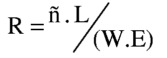
- any resistance value is not necessarily practical to implement, with the type of reading circuit that the system designer intends use, and it is usually more convenient, to optimize the functions of the circuit of reading that this resistance R is determined by constraints specific to this circuit, rather than by constraints generated by the bolometric detector as such.
- this resistance is defined by the relation: where ⁇ is the electrical resistivity of the bolometric material in the vicinity of the operating temperature.
- the configuration of the electrode (5) directly defines the width W and length L and interdigitation, as for example shown in FIGS. 1 and 2 and offers a certain degree of freedom.
- the configuration of the current lines in the context of Figure 2 can be modeled on the one hand, the three rectangular zones bordered by the parts (6B) in their rectilinear parallel portion, on the other hand, the two zones (8) corresponding to the ends of the portions (6B) internal to the bolometric detector.
- the density of the current lines is uniform and local quantities W r and L r are immediately defined, in which the index r relates to the rectangular areas.
- the density of the current lines is variable, namely significantly higher in the vicinity of the peaks of the zones (6B) than inside the rectangular areas, and significantly weaker in the vicinity of the opposite portion (6B).
- r 1 can be likened to the half-width of the elongated pattern of the parts (6B) of FIG.
- the total effective "electrical" width W Wp + Wr (in solid line along the central equipotential between parts (6B)) would be close to 60 microns for a maximum electrical width (shown in dashed lines) of about 73 microns. This difference represents a loss of about 11% of performance compared to an ideal bolometric detector, which would not show localized spike effects.
- the configuration proposed in this document besides the disadvantages already mentioned, is likely to improve in terms of the thermal resolution of the bolometric detector.
- US Pat. No. 5,367,167 also discloses a bolometric detector comprising two coplanar electrodes located on the same face of the bolometric material, as well as a conductive layer on the other side of this layer of bolometric material.
- This conductive layer has the function of absorbing infrared radiation that one wishes to detect and must be separated from the body of the detector by an electrically insulating layer. It is therefore of a complexity high for its realization.
- the arrangement of the electrodes so remote reduces the application of this bolometric detector to the materials bolometric low resistivity, such as typically vanadium oxides.
- the object of the present invention is a bolometric construction detector simple, whose mass distribution of the bolometric material on the surface of the elementary detector is controlled, so that all or almost all of the mass of said bolometric material is traversed by current lines, and for the purpose to achieve a better level of performance with dimensions and time constant thermal data. It also aims to provide an additional degree of adjustment electrical resistance, constant performance.
- the invention implements one or more undulations, making it possible to increase significantly the amount of bolometric material traversed by the current lines, and in doing so, optimizes detector performance, especially in terms of thermal resolution, without increasing the mass of bolometric material.
- the invention consists in increasing the proportion useful of the total volume of bolometric material with time constant ⁇ th conserved.
- increasing the thickness of said bolometric material in order to to increase the useful volume of this material is not a free parameter of optimization, given the then correlative increase in this constant of time.
- these undulations can be parallel or perpendicular or the two at a time on areas separated from the current lines that cross the structure, Operating. They may still be oblique with respect to the said lines of current.
- the amplitude of the undulations is less than the distance separating electrodes of the constituent substrate of the reading circuit, and is in particular at most equal to 1.5 ⁇ m.
- the invention also relates to an infrared detection device implementing such a bolometric detector.
- the detector or detectors are joined together to the reading circuit by means of a pillar type structure (3).
- this device has a matrix structure comprising at least two bolometric detectors.
- It also relates to a method of manufacturing such a bolometric detector.
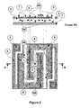
- FIG. 3a therefore shows the central part of a detector bolometric device according to the invention, in particular the radiation-sensitive part infrared that such a detector is intended to detect.
- the parts (6A) of the bolometric material that is to say the electrode-free portions (5) have corrugations on their entire surface (9) oriented perpendicular to the plane comprising said sensitive portion, and such it can be seen on section A-A, shown in Figure 3a.
- corrugations are defined by a pitch P and an amplitude D.
- F is defined as being the ratio between the extended length of a corrugation (9) and the pitch P
- the corrugations (9) are oriented perpendicular to the direction of the current. According to this configuration, there is an increase in the resistance R in the ratio F, and an improvement in the thermal resolution NedT also in the ratio F 1/2 .
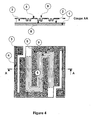
- FIG. 4 illustrates the application of the invention to the bolometric detector of FIG. 1, ie the bolometric detector reproducing the teachings of the document FR-A-2 752 299, in this case according to the embodiment defined in Figure 3b.
- the objective is to search for an improvement of the thermal resolution NedT with thickness E of material constant bolometric.
- this configuration makes it possible to keep the thermal resistance constant, especially in the case where the structures (4) of thermal insulation are essentially constituted by the layer of bolometric material (6).
- the improvement of the thermal resolution NedT is of the order of 54% if we take into account account the increase in RTh resulting from the decrease in thickness of the layer (6).
- the insulation structures (4) are made so essentially independent of the thickness of the bolometric material layer (6), which implies a much more complex construction architecture, and performed in such a way as to maintain the reference RTh, it is then advantageous to decrease the thickness of said layer (6) of bolometric material in the central portion of bolometer, and simultaneously, increase the ripple factor F to maintain constant the mass of bolometric material (so ⁇ th), while improving the thermal resolution.
- FIG. implement the invention according to the configuration of the bolometric detector of the prior art as shown in Figure 2.
- the ends of the narrow zones (6B) have been modified with respect to this prior art, in particular by the insertion of a disk or a substantially regular polygon, of radius r 2 , substantially greater than half the width of the elongated portion (6B) (denoted r 1 above).
- the portion (6B) opposite is preferably rounded or polygonal, as illustrated in Figure 5, to make the distance between the two parts (6B) roughly constant, with the aim of maximizing the total current crossing the structure without generating any area where current intensity would be significantly higher than the average.
- At least one corrugation (9) is produced in the interval between two parts (6B), so that the "electrical" length deployed between these two parts is substantially equal to L.
- the corrugations can be continued at one or rectangular zones, under various reserves of mass and optical absorption disturbances, as previously reported.
- the rectangular zones are reduced by approximately 33 ⁇ m of electric width Wr by following the insertion of the circular zones (8), according to the example described.
- the width resulting overall electric W Wp + Wr being then close to 80 microns.
- this bolometer is carried out by successive deposits and engravings with the aid of traditional processes known to those skilled in the art, particularly in the field of microelectronics, various layers constituting the finished product (dielectrics, bolometric material, metallic materials for equipotential areas or electrodes).
- the invention can be implemented only for this purpose of resistance adjustment in a given space, by another as the adjustment of thickness, resistivity, equipotential (6B).
- a deposit is made of reflective metal layer, and a first lithographic level is applied to separate by etching the reflector patterns.
- the sacrificial layer typically polyimide.
- the conventional treatment of the sacrificial layer typically polyimide.
- the sacrificial layer typically polyimide.
- the sacrificial layer typically polyimide.
- the deposit optional polyimide surface of an insulator typically oxide or silicon nitride (10 to 100 nanometers thick).
- the conductive layer (5) typically nitride nitride, is then deposited.
- titanium in order to obtain a resistance of layers of 150 to 400 Ohms, and one applies a second lithographic mask and etching of the layer (5) in clearing the surfaces where the undulations (9) will be engraved.
- a fourth lithographic mask is then applied to engrave in the layers superficial and polyimide, the impression of the pillars (3).
- a metallic material is then deposited according to the known techniques, to form the pillars (3) and a fifth lithographic mask is applied to engrave this metallic material outside the parts (3).
- the profile of the undulations is defined by the techniques of detail of the masking and control of the etching process, well known to those skilled in the art. Training undulations during the process rather than before any surface deposition of the polyimide has the advantage of eliminating all or part of the mass of non affected by the current lines (here one or two dielectric layers) on the surfaces affected by the etching of the undulations.
- the deposit of the bolometric material typically but not limited to amorphous silicon or related material of the Si x Ge y C z type, where x, y and z have a value between 0 and 1, with x + y +, is then deposited.
- z 1, this material being dopable with boron or phosphorus and extending over a thickness of between 50 and 300 nanometers.
- the bolometric material may also consist of vanadium oxide or mixture of vanadium oxides of various compositions (of general formula VOx).
- An important criterion of successful application of the present invention is the good recovery of the corrugation by the bolometric material, which can be obtained without difficulty, in particular with amorphous silicon and related materials, synthesized very generally by chemical deposition in the vapor phase (CVD for Chemical Vapor Deposition ).
- a seventh level of lithography to define the outline of elementary detectors, thermal isolation arms (4) and protect the pillars (3) and engraving of all the layers present outside the pillars (3) to the sacrificial layer.
- a lithographic level additional can be applied before the seventh previous level, in order to eliminate the bolometric material on the surface corresponding to the parts (3), and this for improve the thermal resistance.
- the production process ends with the cutting of substrates into finished products individual, and elimination of the sacrificial layer.
- the realization of the hollow corrugation pattern with respect to the flat surface of the sacrificial layer may also be made in relief.
- the The detector according to the invention is designed in such a way that the current density local is approximately constant on the surface of the active bolometric material (defined by a small part of zones 6A), because the noise would be more important in areas where the current density is higher. This is the reason why ripples are evenly distributed in the available space of the parts (6A) on Figures 3 and 4 and that, moreover, it was made to exceed the pattern (9) ripples on the boundaries of adjacent equipotential portions (5) in Figure 3a. These provisions optimize the result but are not mandatory.
Landscapes
- Physics & Mathematics (AREA)
- General Physics & Mathematics (AREA)
- Spectroscopy & Molecular Physics (AREA)
- Photometry And Measurement Of Optical Pulse Characteristics (AREA)
- Radiation Pyrometers (AREA)
Abstract
Description
- des moyens d'absorption du rayonnement infrarouge et de conversion de ce dernier en chaleur ;
- des moyens d'isolation thermique du détecteur, de telle sorte à permettre à celui-ci de s'échauffer sous l'action du rayonnement infrarouge ;
- des moyens de thermométrie, qui dans le cadre d'un détecteur bolométrique mettent en oeuvre un élément résistif ;
- et des moyens de lecture des signaux électriques fournis par les moyens de thermométrie.
- de la maítrise d'élaboration et d'intégration des matériaux bolométriques les plus performants ;
- de la maítrise de conception et de construction des détecteurs élémentaires, sous la forme de micro-ponts, c'est à dire de structures légères et fragiles isolées thermiquement du circuit de lecture ;
- de la qualité de mise en oeuvre de ces détecteurs et des diverses fonctions de correction qui sont utilisées dans le circuit de lecture et dans d'autres dispositifs annexes ;
- et de la maítrise des techniques de conditionnement dans un boítier étanche sous faible pression.
- K est un paramètre de proportionnalité qu'il n'est pas utile de détailler ici, qui intègre la bande passante du circuit de lecture, le niveau de bruit basse fréquence « en 1/f» du matériau bolomètrique (6), la surface du détecteur élémentaire, et l'efficacité d'absorption infrarouge du détecteur élémentaire ;
- W et L sont respectivement les largeur et longueur électrique des lignes de courant à travers le matériau bolométrique (6), que l'on retrouvera sur les figures 1 et 2 ;
- E est l'épaisseur du matériau bolométrique (6) sur la surface concernée par les lignes de courant limitée par les dimensions W et L ;
- TCR est la variation relative de résistance au voisinage de la température de fonctionnement (dR/RdT), caractéristique du matériau bolométrique mis en oeuvre, où R est la résistance électrique vue entre les deux pôles d'amenée du courant (les deux piliers (3)) et T la température du micro-pont ;
- Rth est la résistance thermique entre la partie centrale « massive » du bolomètre qui s'échauffe sous l'effet du rayonnement infrarouge, et le circuit de lecture (1), dont la température est constante ou très lentement variable.
- une partie sensible comportant :
- une ou plusieurs couches d'un matériau sensible, dont la résistivité varie avec la température ;
- des électrodes isolées les unes des autres faisant en outre fonction d'absorbeur du rayonnement infrarouge, lesdites électrodes étant en contact avec le matériau sensible sur au moins une partie de leur surface ;
- au moins une zone support de la partie sensible, faisant fonction de positionnement de la dite partie sensible, et de conducteur électrique en relation avec un circuit de lecture associé au détecteur bolométrique,
- au moins une structure d'isolement thermique reliant électriquement et mécaniquement chaque zone support à la partie sensible.
- en ce que les zones de matériau sensible non en contact avec les électrodes, présentent au moins une ondulation dans la direction perpendiculaire au plan contenant la partie sensible du détecteur bolométrique ;
- et en ce que le matériau sensible bolométrique est constitué de silicium amorphe ou d'un alliage apparenté de type SixGeyCz où x + y + z = 1.
La largeur Wp du rectangle de longueur « électrique » L équivalent aux deux zones (8) modifiées selon l'invention est donnée par la relation
- formation d'une couche auxiliaire, dite sacrificielle sur le substrat constitutif du circuit de lecture, notamment en silicium, ladite couche étant destinée à être ôtée par tout moyen connu après réalisation du détecteur, afin de découpler thermiquement le circuit de lecture du module de détection, également appelé partie sensible ;
- formation sur cette couche sacrificielle d'une couche de matériau bolométrique, et des électrodes.
Claims (11)
- Détecteur bolométrique comprenant :caractérisé :une partie sensible comportant :une ou plusieurs couches (6) d'un matériau sensible, dont la résistivité varie avec la température ;des électrodes (5) isolées les unes des autres faisant en outre fonction d'absorbeur du rayonnement infrarouge, lesdites électrodes étant en contact avec le matériau sensible sur au moins une partie de leur surface ;au moins une zone support (3) de la partie sensible, faisant fonction de positionnement de la dite partie sensible, et de conducteur électrique en relation avec un circuit de lecture (1) associé au détecteur bolométrique,au moins une structure d'isolement thermique reliant électriquement et mécaniquement chaque zone support (3) à la partie sensible,en ce que les zones de matériau sensible non en contact avec les électrodes (5), présentent au moins une ondulation (9) orientée selon la direction perpendiculaire au plan contenant la partie sensible du détecteur bolométrique ;et en ce que le matériau sensible bolométrique est constitué de silicium amorphe ou d'un alliage apparenté de type SixGeyCz où x+y+z=1.
- Détecteur bolométrique selon la revendication 1, caractérisé en ce que la ou les ondulations (9) sont orientées parallèlement aux lignes de courant qui traversent la partie sensible du détecteur en fonctionnement.
- Détecteur bolométrique selon la revendication 1, caractérisé en ce que la ou les ondulations (9) sont orientées perpendiculairement aux lignes de courant qui traversent la partie sensible du détecteur en fonctionnement.
- Détecteur bolométrique selon la revendication 1, caractérisé en ce qu'il comprend plusieurs zones d'ondulations (9) positionnées au niveau de zones différentes, lesdites ondulations étant respectivement orientées parallèlement et perpendiculairement aux lignes de courant qui traversent la partie sensible du détecteur en fonctionnement.
- Détecteur bolométrique selon la revendication 1, caractérisé en ce que la ou les ondulations (9) sont orientées de manière oblique par rapport aux lignes de courant qui traversent la partie sensible du détecteur en fonctionnement.
- Détecteur bolométrique selon l'une des revendications 1 à 5, caractérisé en ce que l'amplitude des ondulations (9) est inférieure à la distance séparant les électrodes (5) du substrat constitutif du circuit de lecture (1).
- Détecteur bolométrique selon la revendication 6, caractérisé en ce que l'amplitude des ondulations (9) est d'au plus 1,5 µm.
- Détecteur bolométrique selon l'une des revendications 1 à 7, caractérisé en ce que le pas ou la périodicité des ondulations (9) est d'au plus trois micromètres.
- Dispositif de détection infrarouge de type bolométrique, caractérisé en ce qu'il met en oeuvre un ou plusieurs détecteurs bolométriques selon l'une des revendications 1 à 8, et en ce que le ou les détecteurs sont solidarisés au circuit de lecture au moyen d'une structure de type pilier (3).
- Dispositif de détection infrarouge de type bolométrique selon la revendication 9, caractérisé en ce qu'il présente une structure matricielle comportant au moins deux détecteurs bolométriques.
- Procédé pour la réalisation d'un détecteur bolométrique, consistant, à partir d'un circuit de lecture, notamment réalisé sur un substrat silicium (1) :caractérisé en ce que l'on réalise une gravure localisée de la couche sacrificielle correspondant à la forme souhaitée d'ondulations (9) préalablement au dépôt du matériau bolométrique, cette gravure étant réalisée dans les zones où les électrodes (5) ne sont pas en contact avec le matériau bolométrique (6).tout d'abord, à former une première couche auxiliaire sacrificielle sur ledit substrat silicium, destinée à être ôtée par tout moyen connu après réalisation du détecteur afin de découpler thermiquement le circuit de lecture (1) du module de détection ou partie sensible ;puis à former sur cette couche auxiliaire sacrificielle, entre autres une couche de matériau bolométrique en silicium amorphe (6) ou en un matériau apparenté de type SixGeyCz où x + y + z = 1, mais également des électrodes (5), destinées à envoyer des signaux électriques nécessaires au fonctionnement du détecteur bolométrique et à acheminer le signal résultant de la détection du rayonnement infra rouge par ledit bolomètre au niveau du circuit de lecture,
Applications Claiming Priority (2)
| Application Number | Priority Date | Filing Date | Title |
|---|---|---|---|
| FR0312042 | 2003-10-15 | ||
| FR0312042A FR2861172B1 (fr) | 2003-10-15 | 2003-10-15 | Detecteur bolometrique, dispositif de detection infrarouge mettant en oeuvre un tel detecteur bolometrique et procede de fabrication de ce detecteur |
Publications (2)
| Publication Number | Publication Date |
|---|---|
| EP1524507A1 true EP1524507A1 (fr) | 2005-04-20 |
| EP1524507B1 EP1524507B1 (fr) | 2009-05-13 |
Family
ID=34355479
Family Applications (1)
| Application Number | Title | Priority Date | Filing Date |
|---|---|---|---|
| EP04300670A Expired - Lifetime EP1524507B1 (fr) | 2003-10-15 | 2004-10-08 | Détecteur bolométrique, dispositif de détection infrarouge mettant en oeuvre un tel détecteur bolométrique et procédé de fabrication de ce détecteur |
Country Status (7)
| Country | Link |
|---|---|
| US (1) | US7138630B2 (fr) |
| EP (1) | EP1524507B1 (fr) |
| CN (1) | CN1727856B (fr) |
| CA (1) | CA2481056C (fr) |
| DE (1) | DE602004021076D1 (fr) |
| FR (1) | FR2861172B1 (fr) |
| RU (1) | RU2356017C2 (fr) |
Cited By (1)
| Publication number | Priority date | Publication date | Assignee | Title |
|---|---|---|---|---|
| FR3163450A1 (fr) * | 2024-06-18 | 2025-12-19 | Commissariat A L' Energie Atomique Et Aux Energies Alternatives | Détecteur thermique comportant une membrane absorbante suspendue à électrode en boucle |
Families Citing this family (21)
| Publication number | Priority date | Publication date | Assignee | Title |
|---|---|---|---|---|
| WO2006038213A2 (fr) * | 2004-10-04 | 2006-04-13 | Bluebird Optical Mems Ltd. | Pixel a ondes millimetriques et capteurs d'imagerie a reseau de plans focaux constitues d'un tel pixel |
| US7718965B1 (en) * | 2006-08-03 | 2010-05-18 | L-3 Communications Corporation | Microbolometer infrared detector elements and methods for forming same |
| FR2906029B1 (fr) * | 2006-09-18 | 2010-09-24 | Ulis | Dispositif electronique de detection et detecteur comprenant un tel dispositif |
| US7633065B2 (en) * | 2006-10-19 | 2009-12-15 | Sensormatic Electronics, LLC | Conduction structure for infrared microbolometer sensors |
| WO2010058559A1 (fr) * | 2008-11-21 | 2010-05-27 | パナソニック株式会社 | Détecteur de rayonnement et procédé de détection de rayonnement |
| KR20100073073A (ko) * | 2008-12-22 | 2010-07-01 | 한국전자통신연구원 | 적외선 감지 센서 및 그 제조 방법 |
| RU2447411C1 (ru) * | 2010-12-01 | 2012-04-10 | Виктор Акиндинович Солдатенков | Способ измерения температуры, термоэлектронномеханический преобразователь с автоэлектронной эмиссией и способ его изготовления |
| RU2511275C2 (ru) * | 2012-07-16 | 2014-04-10 | Федеральное государственное унитарное предприятие "Научно-исследовательский институт физических проблем им. Ф.В. Лукина" | Наноструктурный ик-приемник (болометр) с большой поверхностью поглощения |
| US9368658B2 (en) * | 2012-08-31 | 2016-06-14 | Robert Bosch Gmbh | Serpentine IR sensor |
| US9297700B2 (en) * | 2012-12-03 | 2016-03-29 | Analog Devices, Inc. | Photonic sensor and a method of manufacturing such a sensor |
| US9199838B2 (en) | 2013-10-25 | 2015-12-01 | Robert Bosch Gmbh | Thermally shorted bolometer |
| FR3056292B1 (fr) * | 2016-09-22 | 2020-11-20 | Commissariat Energie Atomique | Structure de detection de rayonnements electromagnetiques de type bolometre et procede de fabrication d'une telle structure |
| JP6726087B2 (ja) * | 2016-12-14 | 2020-07-22 | 浜松ホトニクス株式会社 | 光検出器 |
| EP3483574A1 (fr) * | 2017-11-14 | 2019-05-15 | Nederlandse Organisatie voor toegepast- natuurwetenschappelijk onderzoek TNO | Microbolomètre et procédé de fabrication |
| US10436646B2 (en) * | 2018-02-28 | 2019-10-08 | Ams Sensors Uk Limited | IR detector arrays |
| FR3089291B1 (fr) * | 2018-11-29 | 2023-03-24 | Commissariat Energie Atomique | Structure de détection de rayonnement électromagnétique à absorption optimisée et procédé de formation d’une telle structure |
| FR3098904B1 (fr) * | 2019-07-16 | 2021-06-18 | Lynred | Micro-bolometre a faible capacite thermique et procede de fabrication associe |
| FR3099573B1 (fr) * | 2019-07-30 | 2021-07-23 | Commissariat Energie Atomique | Procédé de fabrication d’un microbolomètre comportant un matériau sensible à base d’oxyde de vanadium |
| FR3101151B1 (fr) * | 2019-09-24 | 2021-12-17 | Office National Detudes Rech Aerospatiales | Dispositif pour reveler des variations spatiales de polarisation d’un rayonnement electromagnetique |
| CN113188669B (zh) * | 2021-04-29 | 2023-06-27 | 上海翼捷工业安全设备股份有限公司 | 红外吸收复合膜结构及二氧化碳热释电红外探测器 |
| TWI846249B (zh) | 2022-12-29 | 2024-06-21 | 財團法人工業技術研究院 | 垂直整合式紅外線感測裝置及其製造方法 |
Citations (3)
| Publication number | Priority date | Publication date | Assignee | Title |
|---|---|---|---|---|
| US5399897A (en) * | 1993-11-29 | 1995-03-21 | Raytheon Company | Microstructure and method of making such structure |
| FR2752299A1 (fr) * | 1996-08-08 | 1998-02-13 | Commissariat Energie Atomique | Detecteur infrarouge et procede de fabication de celui-ci |
| WO2000037906A1 (fr) * | 1998-12-18 | 2000-06-29 | Daewoo Electronics Co., Ltd. | Bolometre a infrarouge et procede de fabrication associe |
Family Cites Families (5)
| Publication number | Priority date | Publication date | Assignee | Title |
|---|---|---|---|---|
| US5021663B1 (en) | 1988-08-12 | 1997-07-01 | Texas Instruments Inc | Infrared detector |
| US5288649A (en) | 1991-09-30 | 1994-02-22 | Texas Instruments Incorporated | Method for forming uncooled infrared detector |
| FR2781927B1 (fr) * | 1998-07-28 | 2001-10-05 | Commissariat Energie Atomique | Dispositif de detection de rayonnements multispectraux infrarouge/visible |
| FR2796148B1 (fr) | 1999-07-08 | 2001-11-23 | Commissariat Energie Atomique | Detecteur bolometrique a isolation electrique intermediaire et procede de fabrication de ce detecteur |
| JP4009832B2 (ja) * | 2002-05-10 | 2007-11-21 | 日本電気株式会社 | ボロメータ型赤外線固体撮像素子 |
-
2003
- 2003-10-15 FR FR0312042A patent/FR2861172B1/fr not_active Expired - Fee Related
-
2004
- 2004-09-29 CA CA2481056A patent/CA2481056C/fr not_active Expired - Fee Related
- 2004-09-30 US US10/954,828 patent/US7138630B2/en not_active Expired - Fee Related
- 2004-10-08 DE DE602004021076T patent/DE602004021076D1/de not_active Expired - Lifetime
- 2004-10-08 EP EP04300670A patent/EP1524507B1/fr not_active Expired - Lifetime
- 2004-10-14 RU RU2004129916/28A patent/RU2356017C2/ru not_active IP Right Cessation
- 2004-10-15 CN CN200410103859.1A patent/CN1727856B/zh not_active Expired - Fee Related
Patent Citations (4)
| Publication number | Priority date | Publication date | Assignee | Title |
|---|---|---|---|---|
| US5399897A (en) * | 1993-11-29 | 1995-03-21 | Raytheon Company | Microstructure and method of making such structure |
| FR2752299A1 (fr) * | 1996-08-08 | 1998-02-13 | Commissariat Energie Atomique | Detecteur infrarouge et procede de fabication de celui-ci |
| US5912464A (en) * | 1996-08-08 | 1999-06-15 | Commissariat Al'energie Atomique | Infrared detector and manufacturing process |
| WO2000037906A1 (fr) * | 1998-12-18 | 2000-06-29 | Daewoo Electronics Co., Ltd. | Bolometre a infrarouge et procede de fabrication associe |
Cited By (2)
| Publication number | Priority date | Publication date | Assignee | Title |
|---|---|---|---|---|
| FR3163450A1 (fr) * | 2024-06-18 | 2025-12-19 | Commissariat A L' Energie Atomique Et Aux Energies Alternatives | Détecteur thermique comportant une membrane absorbante suspendue à électrode en boucle |
| EP4667885A1 (fr) * | 2024-06-18 | 2025-12-24 | Commissariat à l'Energie Atomique et aux Energies Alternatives | Detecteur thermique comportant une membrane absorbante suspendue a electrode en boucle |
Also Published As
| Publication number | Publication date |
|---|---|
| CA2481056C (fr) | 2013-03-26 |
| DE602004021076D1 (de) | 2009-06-25 |
| FR2861172A1 (fr) | 2005-04-22 |
| CN1727856B (zh) | 2010-05-26 |
| US7138630B2 (en) | 2006-11-21 |
| RU2356017C2 (ru) | 2009-05-20 |
| CN1727856A (zh) | 2006-02-01 |
| US20050082481A1 (en) | 2005-04-21 |
| FR2861172B1 (fr) | 2006-06-02 |
| CA2481056A1 (fr) | 2005-04-15 |
| RU2004129916A (ru) | 2006-03-20 |
| EP1524507B1 (fr) | 2009-05-13 |
Similar Documents
| Publication | Publication Date | Title |
|---|---|---|
| EP1524507B1 (fr) | Détecteur bolométrique, dispositif de détection infrarouge mettant en oeuvre un tel détecteur bolométrique et procédé de fabrication de ce détecteur | |
| EP1703266B1 (fr) | Détecteur bolométrique, dispositif de détection infrarouge mettant en oeuvre un tel détecteur et procédé de fabrication de ce détecteur | |
| EP0828145B1 (fr) | Détecteur infrarouge et procédé de fabrication de celui-ci | |
| EP1653205B1 (fr) | Détecteur bolométrique à isolation thermique par constriction | |
| EP0749007B1 (fr) | Dispositif de détection bolométrique pour ondes millimétriques et submillimétriques et procédé de fabrication de ce dispositif | |
| EP3182081B1 (fr) | Dispositif de detection a membranes bolometriques suspendues a fort rendement d'absorption et rapport signal sur bruit | |
| FR3050526A1 (fr) | Dispositif de detection de rayonnement electromagnetique a structure d’encapsulation comportant au moins un filtre interferentiel | |
| EP2613181A1 (fr) | Détecteur infrarouge comportant un boîtier intégrant au moins un réseau de diffraction | |
| EP3067675B1 (fr) | Dispositif de detection de rayonnement electromagnetique a structure d'encapsulation hermetique a event de liberation | |
| CA2853751A1 (fr) | Detecteur infrarouge a base de micro-planches bolometriques suspendues | |
| CA2515104C (fr) | Dispositif de detection de rayonnements infrarouges a detecteurs bolometriques | |
| FR3017456A1 (fr) | Detecteur bolometrique a structure mim incluant un element thermometre | |
| EP1067372A1 (fr) | Détecteur bolométrique à isolation électrique intermédiaire et procédé pour sa fabrication | |
| CA2959650A1 (fr) | Capteur de motifs thermiques a bolometres sous capsule(s) | |
| CA2637223C (fr) | Detecteur de rayonnement electromagnetique et procede de fabrication d'un tel detecteur | |
| EP2846201B1 (fr) | Dispositif émissif lumineux à structures diffractives et à hologramme synthétique | |
| WO2013189997A1 (fr) | Structure semiconductrice comportant une zone absorbante placee dans une cavite focalisante | |
| EP1880176B1 (fr) | Detecteur thermique de rayonnements electromagnetiques et dispositif de detection infrarouge mettant en oeuvre de tels detecteurs | |
| CA2658035C (fr) | Detecteur thermique a haute isolation | |
| EP4553465A1 (fr) | Detecteur thermique large bande et a plusieurs cavites quart d'onde | |
| WO2019043312A1 (fr) | Detecteur de rayonnement electromagnetique | |
| FR3066017A1 (fr) | Dispositif pyroelectrique de detection infrarouge comportant un emetteur infrarouge de modulation | |
| FR3055412A1 (fr) | Capteur de motifs thermiques par imagerie infrarouge d'une matrice d'elements chauffants. |
Legal Events
| Date | Code | Title | Description |
|---|---|---|---|
| PUAI | Public reference made under article 153(3) epc to a published international application that has entered the european phase |
Free format text: ORIGINAL CODE: 0009012 |
|
| AK | Designated contracting states |
Kind code of ref document: A1 Designated state(s): AT BE BG CH CY CZ DE DK EE ES FI FR GB GR HU IE IT LI LU MC NL PL PT RO SE SI SK TR |
|
| AX | Request for extension of the european patent |
Extension state: AL HR LT LV MK |
|
| 17P | Request for examination filed |
Effective date: 20050525 |
|
| AKX | Designation fees paid |
Designated state(s): DE FR GB IT SE |
|
| 17Q | First examination report despatched |
Effective date: 20071023 |
|
| GRAP | Despatch of communication of intention to grant a patent |
Free format text: ORIGINAL CODE: EPIDOSNIGR1 |
|
| GRAS | Grant fee paid |
Free format text: ORIGINAL CODE: EPIDOSNIGR3 |
|
| GRAA | (expected) grant |
Free format text: ORIGINAL CODE: 0009210 |
|
| AK | Designated contracting states |
Kind code of ref document: B1 Designated state(s): DE FR GB IT SE |
|
| REG | Reference to a national code |
Ref country code: GB Ref legal event code: FG4D Free format text: NOT ENGLISH |
|
| REF | Corresponds to: |
Ref document number: 602004021076 Country of ref document: DE Date of ref document: 20090625 Kind code of ref document: P |
|
| REG | Reference to a national code |
Ref country code: SE Ref legal event code: TRGR |
|
| PLBE | No opposition filed within time limit |
Free format text: ORIGINAL CODE: 0009261 |
|
| STAA | Information on the status of an ep patent application or granted ep patent |
Free format text: STATUS: NO OPPOSITION FILED WITHIN TIME LIMIT |
|
| 26N | No opposition filed |
Effective date: 20100216 |
|
| PGFP | Annual fee paid to national office [announced via postgrant information from national office to epo] |
Ref country code: IT Payment date: 20131011 Year of fee payment: 10 |
|
| PG25 | Lapsed in a contracting state [announced via postgrant information from national office to epo] |
Ref country code: IT Free format text: LAPSE BECAUSE OF NON-PAYMENT OF DUE FEES Effective date: 20141008 |
|
| REG | Reference to a national code |
Ref country code: FR Ref legal event code: PLFP Year of fee payment: 12 |
|
| REG | Reference to a national code |
Ref country code: FR Ref legal event code: PLFP Year of fee payment: 13 |
|
| REG | Reference to a national code |
Ref country code: FR Ref legal event code: PLFP Year of fee payment: 14 |
|
| REG | Reference to a national code |
Ref country code: FR Ref legal event code: PLFP Year of fee payment: 15 |
|
| PGFP | Annual fee paid to national office [announced via postgrant information from national office to epo] |
Ref country code: SE Payment date: 20181022 Year of fee payment: 15 Ref country code: DE Payment date: 20181009 Year of fee payment: 15 |
|
| PGFP | Annual fee paid to national office [announced via postgrant information from national office to epo] |
Ref country code: FR Payment date: 20181027 Year of fee payment: 15 Ref country code: GB Payment date: 20181017 Year of fee payment: 15 |
|
| REG | Reference to a national code |
Ref country code: DE Ref legal event code: R119 Ref document number: 602004021076 Country of ref document: DE |
|
| PG25 | Lapsed in a contracting state [announced via postgrant information from national office to epo] |
Ref country code: DE Free format text: LAPSE BECAUSE OF NON-PAYMENT OF DUE FEES Effective date: 20200501 |
|
| PG25 | Lapsed in a contracting state [announced via postgrant information from national office to epo] |
Ref country code: SE Free format text: LAPSE BECAUSE OF NON-PAYMENT OF DUE FEES Effective date: 20191009 |
|
| GBPC | Gb: european patent ceased through non-payment of renewal fee |
Effective date: 20191008 |
|
| PG25 | Lapsed in a contracting state [announced via postgrant information from national office to epo] |
Ref country code: FR Free format text: LAPSE BECAUSE OF NON-PAYMENT OF DUE FEES Effective date: 20191031 Ref country code: GB Free format text: LAPSE BECAUSE OF NON-PAYMENT OF DUE FEES Effective date: 20191008 |