EP1523068B1 - Contact à fiche , procédé et appareil de fabrication - Google Patents
Contact à fiche , procédé et appareil de fabrication Download PDFInfo
- Publication number
- EP1523068B1 EP1523068B1 EP04104747A EP04104747A EP1523068B1 EP 1523068 B1 EP1523068 B1 EP 1523068B1 EP 04104747 A EP04104747 A EP 04104747A EP 04104747 A EP04104747 A EP 04104747A EP 1523068 B1 EP1523068 B1 EP 1523068B1
- Authority
- EP
- European Patent Office
- Prior art keywords
- contact
- squeezing
- feed
- deformable portion
- hole
- Prior art date
- Legal status (The legal status is an assumption and is not a legal conclusion. Google has not performed a legal analysis and makes no representation as to the accuracy of the status listed.)
- Expired - Lifetime
Links
- 238000004519 manufacturing process Methods 0.000 title claims description 13
- 238000000034 method Methods 0.000 title claims description 13
- 238000003780 insertion Methods 0.000 claims description 10
- 230000037431 insertion Effects 0.000 claims description 10
- 230000000694 effects Effects 0.000 claims description 3
- 238000006073 displacement reaction Methods 0.000 description 8
- 238000003825 pressing Methods 0.000 description 5
- 230000003068 static effect Effects 0.000 description 3
- 230000000295 complement effect Effects 0.000 description 1
- 239000002184 metal Substances 0.000 description 1
Images


Classifications
-
- H—ELECTRICITY
- H01—ELECTRIC ELEMENTS
- H01R—ELECTRICALLY-CONDUCTIVE CONNECTIONS; STRUCTURAL ASSOCIATIONS OF A PLURALITY OF MUTUALLY-INSULATED ELECTRICAL CONNECTING ELEMENTS; COUPLING DEVICES; CURRENT COLLECTORS
- H01R12/00—Structural associations of a plurality of mutually-insulated electrical connecting elements, specially adapted for printed circuits, e.g. printed circuit boards [PCB], flat or ribbon cables, or like generally planar structures, e.g. terminal strips, terminal blocks; Coupling devices specially adapted for printed circuits, flat or ribbon cables, or like generally planar structures; Terminals specially adapted for contact with, or insertion into, printed circuits, flat or ribbon cables, or like generally planar structures
- H01R12/50—Fixed connections
- H01R12/51—Fixed connections for rigid printed circuits or like structures
- H01R12/55—Fixed connections for rigid printed circuits or like structures characterised by the terminals
- H01R12/58—Fixed connections for rigid printed circuits or like structures characterised by the terminals terminals for insertion into holes
- H01R12/585—Terminals having a press fit or a compliant portion and a shank passing through a hole in the printed circuit board
-
- Y—GENERAL TAGGING OF NEW TECHNOLOGICAL DEVELOPMENTS; GENERAL TAGGING OF CROSS-SECTIONAL TECHNOLOGIES SPANNING OVER SEVERAL SECTIONS OF THE IPC; TECHNICAL SUBJECTS COVERED BY FORMER USPC CROSS-REFERENCE ART COLLECTIONS [XRACs] AND DIGESTS
- Y10—TECHNICAL SUBJECTS COVERED BY FORMER USPC
- Y10T—TECHNICAL SUBJECTS COVERED BY FORMER US CLASSIFICATION
- Y10T29/00—Metal working
- Y10T29/49—Method of mechanical manufacture
- Y10T29/49002—Electrical device making
- Y10T29/49117—Conductor or circuit manufacturing
- Y10T29/49124—On flat or curved insulated base, e.g., printed circuit, etc.
- Y10T29/49147—Assembling terminal to base
- Y10T29/49151—Assembling terminal to base by deforming or shaping
- Y10T29/49153—Assembling terminal to base by deforming or shaping with shaping or forcing terminal into base aperture
Definitions
- the present invention relates to a method of manufacturing a pin contact for electrical engagement with a lining of a conductively lined hole in a circuit board.
- the present invention also relates to such a contact and an apparatus for its manufacture.
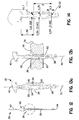
- FIG. 1 A prior art pin contact 1 is shown in Fig 1 .
- the pin contact 1 includes a feed-through portion 2 for insertion through a hole 10 (see Fig 5 ) in a circuit board 12 and a deformable portion 4 (an enlarged view 8 of which is shown in Fig 2 ) at an end of the feed-through portion 2.
- the deformable portion 4 is adapted to be forced into a conductive lining 14 in the hole 10 which is electrically connected to a layer 16 in the board 12.
- a plurality of pin contacts are usually mounted in a connector with their feed through portions 2 projecting therefrom.
- the feed-through portions 2 of the connectors are threaded into a plurality of lined holes 10 in the board and as the connector is moved towards the board the deformable portions 4 of the connectors are deformed as described above.
- Customarily a shroud or other device with a plurality of closely spaced holes for receipt of the feed-through portions is threaded over the feed-through portions 2. As each deformable portion 4 of a connector is pressed into a hole lining it is squeezed.
- each contact 1 tends to become misaligned with the deformable portion 4 thereof.
- the deformable portion may not be symmetrically formed with respect to a central longitudinal plane thereof, for example in the case of a so-called eye of a needle pin contact, of the type shown in Fig 1 , an aperture 18 in the deformable portion 4 may not be exactly centrally located with respect to a width of the contact and the thickness of sections 20 on either side of the deformable portion 4 may not be equal.
- Such asymmetry causes the feed-through portion 2 to become bent away from a central longitudinal axis 22 of the contact 1 so that its tip 24 becomes displaced by a distance d shown in Fig 3 from the axis 22.
- Figs 3 and 4 show the shape of the contact after it has been partially inserted into the hole 10.
- the board 12 is shown schematically in dashed lines in Figs 3 and 4 .
- Such displacement of the tips 24 of typical prior art contacts which have been pressed into holes of various different diameters (a- 0.65mm, b- 0.70mm, c- 0.75mm,d- 0.80mm) is demonstrated in Fig 7 . It can be seen that when the contacts are pressed into relatively small holes their tips 24 tend to be displaced to a greater extent. Due to manufacturing tolerances for printed circuit boards a certain range of hole diameters should work.
- the disadvantage of pressing the contacts into relatively larger diameter holes, as shown in figure 7d is that the electrical connection between the contacts and the conductive linings 14 is less effective. There is usually a requirement to mount a shroud or other device with a plurality of closely spaced holes over the feed-through portions of the contacts which often proves difficult or even impossible as a consequence of the displacement of the tips 24.
- the misalignment could also be in a direction perpendicular to the one shown in Fig 3 which results in the same problem when a shroud is to be mounted over the pin.
- the feed-through portion may rotate. If the rotation is high, electrical connection to the feed-through portion can not be guaranteed.
- the object of the invention is to provide a solution to the above problem.
- a method of making a pin type contact for electrical engagement with a lining of a conductively lined hole in a circuit board comprising the steps of: (a) forming a pin contact with a feed-through portion for insertion through the hole in the circuit board and a deformable portion at one end of the feed-through portion for engaging the lining of the hole; and (b) squeezing an end of the deformable portion which is adjacent to the feed-through portion prior to engagement of the deformable portion with the hole lining.
- the squeezing step may be replaced by applying a deformation similar to partial insertion of the deformable portion into the hole.
- the inventor has discovered that the majority of the displacement of the contact tip is caused as a leading part of the deformable portion is pressed into the hole.
- a contact with no or substantially no tip displacement resulting from the squeezing or partial deformation of the leading part of the deformable portion can be provided to a board manufacturer.
- the contact will be in a condition in which it can be pressed into a hole in a board and undergo virtually no tip displacement since deformation of other parts of the deformable portion have very little effect on tip displacement.
- This makes it easy for the board manufacturer to mount a shroud or other similar device over the feed-through portions of a plurality of contacts which have been pressed into holes in the board.
- the method comprising the further step after step b of straightening misalignment of the portions of the contact resulting from the squeezing or partial deformation step so that said contact portions are substantially aligned along a central longitudinal axis of the contact.
- any tip displacement occurring during the squeezing step can be corrected.
- the portions of the contact may be held in longitudinal alignment as the squeezing step is effected.
- a typical example of the invention is a so-called eye of the needle contact with a gap situated in a region occupied by the deformable portion and the squeezing step involves reducing a width of the gap at one end part thereof as shown for example in Figure 14 .
- the method includes an additional step, prior to the squeezing step, of positioning a support member between parts of the spaced sections not to be squeezed together.
- a support member may not be necessary.
- a method of making mechanical and electrical engagement with a conductive lining in a hole in a circuit board comprising making a pin type contact as mentioned above, inserting the feed-through portion through the hole and then forcing the deformable portion into the hole thereby deforming it and forming the mechanical and electrical engagement between the lining and the contact.
- a method of making an electrical connector involving making a plurality of contacts as mentioned above and fixing them in a connector housing with the feed-through portions of the contacts projecting from the housing.
- a method of making mechanical and electrical engagement with conductive linings in holes in a circuit board comprising making a connector as mentioned above, inserting the feed-through portions of the contacts through the holes and then forcing the deformable portions of the contacts into the holes thereby deforming them and forming the mechanical and electrical engagements between the linings and the contacts.
- pin contact for engagement with a conductive lining of a conductively lined hole of a circuit board comprising a feed-through portion for insertion through the hole and a deformable portion at one end of the feed-through portion for engaging the hole wherein, prior to engagement of the deformable portion with the conductive lining, an end of the deformable portion which is adjacent the feed-through portion is squeezed or deformed.
- the squeezing or deformation is less than would result in full insertion into the hole.
- the deformation corresponds to that which would result from partial insertion of the deformable portion into the hole.
- the deformation could be similar to that caused by insertion into bigger holes.
- the pin contact is a so-called eye of a needle type contact
- the deformable portion includes a gap and the squeezed end part of the deformable portion includes an at least substantially closed section of the gap.
- Such a pin contact has been found to exhibit virtually no tip displacement when inserted into a hole of a board.
- an apparatus for forming a pin contact for electrical engagement with a conductive lining of a conductively lined hole in a circuit board including forming means for forming a pin contact with a feed-through portion and a deformable portion at one end of the feed-through portion for engagement with the conductive lining and a squeezing means adapted to squeeze an end part of the deformable portion which is adjacent to the feed-through portion.
- Such apparatus can be used to make a pin contact having the advantages mentioned in the context of the first aspect of the invention.
- the squeezing means includes restraint means for holding the portions of the contact longitudinally aligned with each other so that when the contact is removed from the squeezing means no subsequent straightening or at least substantially less straightening of the contact portions is required.
- the squeezing apparatus includes a support member arranged to hold two sections of the deformable portion apart as the squeezing is effected.
- the squeezing means includes two squeezing members which are displaceable towards and away from each other and which include cam surfaces, the squeezing means further including camming means which is engageable with the cam surfaces so as to urge the squeezing members towards each other to effect the squeezing.
- camming means which is engageable with the cam surfaces so as to urge the squeezing members towards each other to effect the squeezing.
- the invention will be described with particular reference to a so-called eye of a needle pin contact 30 of the type shown in Fig 12 having a deformable portion 36 which includes a gap or gap 32 between two side sections 34, a feed-through portion 38 extending from one end of the deformable portion 36 and a terminal portion 40 extending from the opposite end of the deformable portion 36.
- the terminal portion 40 includes a root 42 where it joins the deformable portion 36 by which the terminal is connected to other similar pin contacts during at least some phases of its manufacture. The roots 42 are separated from each other prior to pressing the contacts into holes in a circuit board.
- a strip 44 of pin contacts 30, each having the features referred to above, will be punched or otherwise formed from a sheet of stock metal with adjacent contacts joined by their roots 42 as shown in Fig 9 .
- a squeezing means or apparatus 46 is then used to squeeze an end part 48 of the deformable portion 36 of each contact 30 which is adjacent to the feed-through portion 38.
- the squeezing apparatus 46 includes first and second static parts 56 and 58 between which two displaceable jaws blocks 60 are provided each of which has an upstanding jaw 62 projecting therefrom with an outwardly facing cam surface 64 and a pivot pin about which it is pivotable.
- the two cam surfaces 64 are engageable by downward movement of a camming means or block 68 which has a downwardly open cam slot 66 formed in a lower surface thereof.
- the squeezing apparatus 46 includes a support member 50 shown in Fig 11 which projects upwards between the jaws 62 and is positioned so that it occupies a part 49 of the gap 32 which is not the end part 48 of the gap to be squeezed.
- the first static part 56 includes restraint means in the form of four first up-stands 52 which engage the root 42 of the contact between the jaws 60.
- the second static part 58 includes restraint means in the form of two second up-stands 54 defining a slot 55 therebetween in which the feed-through portion 38 of the contact is snugly accommodated.
- the purpose of the up-stands is to prevent distortion of the contact and in particular the feed-through portion from occurring when squeezing of the end part 48 occurs.
- Photographs of the deformable portion of the contact before and after this squeezing operation are shown respectively in Figs 15 and 16 .
- the feed-through portion 38 becomes misaligned with respect to a central longitudinal axis 70 of the contact, this misalignment can be corrected after the strip 44 of contacts has been removed from the squeezing apparatus 46.
- the contacts can be supplied to a customer connected to each other as a strip 44 or separated from each other.
- a plurality of contacts 30 may be mounted in a housing 72 to form a connector 74 with their terminal portions 40 and feed-through portions 38 projecting from opposite sides of the housing as shown in Fig 18 .
- the feed through portion 38 is threaded through a hole 82 in the lining 76 until the squeezed end part 48 of the deformable portion 36 is just inside the hole 82.
- the deformable portion 36 is then pressed fully or substantially fully into the hole 82 to the position shown in Fig 13b which causes the gap 32 to at least substantially close up as shown by reference numeral 33.
- Fig 17 shows a photograph of the feed-through portions 38 of contacts (having 0.04 mm lateral deviation of the gap from the contact centreline) which have been prepared in accordance with the invention after the contacts have been pressed into complementary holes in a 4.6 mm thick circuit board 78. It can be seen that the feed-through portions are all well aligned with each other and perpendicular to the surface of the circuit board.
Landscapes
- Coupling Device And Connection With Printed Circuit (AREA)
- Multi-Conductor Connections (AREA)
- Manufacturing Of Electrical Connectors (AREA)
Claims (16)
- Procédé de fabrication d'un contact mâle (30) pour l'engagement électrique avec un revêtement intérieur (76) d'un trou garni d'un revêtement intérieur conducteur (80) dans une carte de circuit imprimé comprenant les étapes consistant à:(a) former un contact mâle (30) avec une partie de traversée (38) pour insertion à travers le trou (80) dans la carte de circuit imprimé (78) et une partie déformable (36) à une partie d'extrémité de la partie de traversée (3 8) pour engager le revêtement intérieur (76) du trou (80); et(b) comprimer ou déformer partiellement une partie d'extrémité (48) de la partie déformable (36) qui est adjacente à la partie de traversée (38) avant l'engagement de la partie déformable (36) avec le revêtement intérieur de trou (76).
- Procédé selon la revendication 1 comprenant l'autre étape après l'étape b consistant à redresser le désalignement des parties (36, 38) du contact (30) résultant de l'étape de compression de sorte que lesdites parties de contact (36, 38) sont sensiblement alignées le long d'un axe longitudinal central (70) du contact (30).
- Procédé selon la revendication 1 ou 2, dans lequel l'étape de compression implique la réduction d'un écartement (32) entre des sections espacées (34) de la partie déformable (36).
- Procédé selon la revendication 3, dans lequel l'étape de compression implique l'étape consistant à fermer sensiblement la partie d'extrémité (48) de l'écartement (32).
- Procédé selon la revendication 3 ou 4, comprenant une étape supplémentaire, avant l'étape de compression, consistant à positionner un élément de support (50) entre les parties des sections espacées (34) ne devant pas être comprimées et rapprochées l'une de l'autre pendant l'étape de compression.
- Procédé selon la revendication 3, 4 ou 5, dans lequel le contact est ce que l'on appelle le chas d'un contact à aiguille avec un écartement (32) situé dans une région occupée par la partie déformable (36) et l'étape de compression implique la réduction d'une largeur de l'écartement (32) à l'une de ses parties d'extrémité.
- Procédé selon l'une quelconque des revendications précédentes, dans lequel, pendant l'étape de compression, les parties (36, 38) du contact (30) sont maintenues en alignement longitudinal l'une par rapport à l'autre.
- Procédé de réalisation d'un engagement électrique avec un revêtement intérieur conducteur (76) dans un trou (80) dans une carte de circuit imprimé (78) comprenant les étapes consistant à fabriquer un contact mâle (30) selon l'une quelconque des revendications précédentes, insérer la partie de traversée (38) à travers le trou (80) et forcer ensuite la partie déformable (36) dans le trou (80), la déformant ainsi et formant l'engagement électrique entre le revêtement intérieur (76) et le contact (30).
- Procédé de fabrication d'un connecteur électrique (74) impliquant la fabrication d'une pluralité de contacts (30) selon l'une quelconque des revendications 1 à 7 et leur fixation dans un boîtier de connecteur (72), les parties de traversée (38) des contacts (30) faisant saillie du boîtier (72).
- Procédé de réalisation d'un engagement électrique avec des revêtement intérieurs conducteurs (76) dans des trous (80) dans une carte de circuit imprimé (78) comprenant les étapes consistant à fabriquer un connecteur (74) selon la revendication 9, insérer les parties de traversée (38) des contacts (30) à travers les trous (80) et forcer ensuite les parties déformable (36) des contacts (30) dans les trous (80), les déformant ainsi et formant les engagements électriques entre les revêtements intérieurs (76) et les contacts (30).
- Contact mâle (30) pour engagement avec un revêtement intérieur conducteur (76) d'un trou garni d'un revêtement intérieur conducteur (80) d'une carte de circuit imprimé (78) comprenant une partie de traversée (38) pour insertion à travers le trou (80) et une partie déformable (36) à une extrémité de la partie de traversée (38) pour engager le trou (80), dans lequel, avant l'engagement de la partie déformable (36) avec le revêtement intérieur conducteur (76), une extrémité (48) de la partie déformable (36) qui est adjacente à la partie de traversée (38) est comprimée.
- Contact mâle (30) selon la revendication 11, dans lequel le contact mâle (30) est ce que l'on appelle le chas d'un contact à aiguille, la partie déformable (36) comprend un écartement (32) et la partie d'extrémité comprimée (48) de la partie déformable (36) comprend une section au moins sensiblement fermée de l'écartement (32).
- Dispositif de formation d'un contact mâle (30) pour engagement électrique avec un revêtement intérieur conducteur (76) d'un trou garni d'un revêtement intérieur conducteur (80) dans une carte de circuit imprimé (78) comprenant un moyen de formation pour former un contact mâle avec une partie de traversée (38) et une partie déformable (36) à une extrémité de la partie de traversée (38) pour engagement avec le revêtement intérieur conducteur (76) et un moyen de compression (46) conçu pour comprimer une partie d'extrémité (48) de la partie déformable (36) qui est adjacente à la partie de traversée (38).
- Dispositif selon la revendication 13, dans lequel le moyen de compression (46) comprend des moyens de retenue (52, 54, 55) pour maintenir les parties (36, 38, 42) du contact (30) alignées longitudinalement les unes avec les autres.
- Dispositif selon la revendication 13 ou 14, dans lequel le moyen de compression (46) comprend un élément de support (50) configuré pour maintenir écartées deux sections (34) de la partie déformable (36) pendant que la compression est effectuée.
- Dispositif selon la revendication 13, 14 ou 15, dans lequel le moyen de compression (46) comprend deux éléments de compression (62) qui sont déplaçables pour se rapprocher et s'éloigner l'un de l'autre et qui comprennent des surfaces de came (64), le moyen de compression (46) comprenant en outre un moyen de calage de came (68) qui peut être engagé avec les surfaces de came (64) de façon à solliciter les éléments de compression (62) l'un vers l'autre pour effectuer la compression.
Priority Applications (3)
| Application Number | Priority Date | Filing Date | Title |
|---|---|---|---|
| EP04104747A EP1523068B1 (fr) | 2003-10-06 | 2004-09-29 | Contact à fiche , procédé et appareil de fabrication |
| PL04104747T PL1523068T3 (pl) | 2003-10-06 | 2004-09-29 | Wtyk szpilkowy oraz sposób i urządzenie do jego wytwarzania |
| US10/958,757 US7240427B2 (en) | 2003-10-06 | 2004-10-05 | Pin contact and method and apparatus for its manufacture |
Applications Claiming Priority (3)
| Application Number | Priority Date | Filing Date | Title |
|---|---|---|---|
| EP03256290 | 2003-10-06 | ||
| EP32562902 | 2003-10-06 | ||
| EP04104747A EP1523068B1 (fr) | 2003-10-06 | 2004-09-29 | Contact à fiche , procédé et appareil de fabrication |
Publications (3)
| Publication Number | Publication Date |
|---|---|
| EP1523068A2 EP1523068A2 (fr) | 2005-04-13 |
| EP1523068A3 EP1523068A3 (fr) | 2007-02-14 |
| EP1523068B1 true EP1523068B1 (fr) | 2008-03-05 |
Family
ID=34621562
Family Applications (1)
| Application Number | Title | Priority Date | Filing Date |
|---|---|---|---|
| EP04104747A Expired - Lifetime EP1523068B1 (fr) | 2003-10-06 | 2004-09-29 | Contact à fiche , procédé et appareil de fabrication |
Country Status (3)
| Country | Link |
|---|---|
| US (1) | US7240427B2 (fr) |
| EP (1) | EP1523068B1 (fr) |
| PL (1) | PL1523068T3 (fr) |
Families Citing this family (6)
| Publication number | Priority date | Publication date | Assignee | Title |
|---|---|---|---|---|
| EP1357151A1 (fr) * | 2002-04-26 | 2003-10-29 | ATOFINA Research | Procédé amélioré pour polymères bimodaux |
| WO2013023877A1 (fr) * | 2011-07-21 | 2013-02-21 | Fci Automotive Holding | Procédé de pré-déformation d'une broche de contact, utilisation d'un dispositif de pré-déformation et broche de contact |
| US9265150B2 (en) * | 2014-02-14 | 2016-02-16 | Lear Corporation | Semi-compliant terminals |
| JP6550890B2 (ja) * | 2015-04-22 | 2019-07-31 | 住友電装株式会社 | プレスフィット端子 |
| JP6735263B2 (ja) * | 2017-11-01 | 2020-08-05 | 矢崎総業株式会社 | プレスフィット端子及び回路基板のプレスフィット端子接続構造 |
| CN108682979A (zh) * | 2018-06-28 | 2018-10-19 | 深圳东金汽车电子有限公司 | 一种免焊接端子 |
Family Cites Families (14)
| Publication number | Priority date | Publication date | Assignee | Title |
|---|---|---|---|---|
| US3374455A (en) * | 1965-10-21 | 1968-03-19 | Dennis J. Sullivan | Electrical connector |
| US3488628A (en) * | 1967-09-27 | 1970-01-06 | Amp Inc | Electrical interconnecting system and parts |
| US3545606A (en) * | 1968-06-11 | 1970-12-08 | Benny Morris Bennett | Flexible tape terminal assembly |
| US3850493A (en) * | 1971-09-24 | 1974-11-26 | Trw Inc | Multiway connector for a printed circuit board |
| DE2234960C3 (de) * | 1971-11-26 | 1975-04-30 | Teledyne, Inc., Los Angeles, Calif. (V.St.A.) | Elektrischer Stecker |
| US3848120A (en) * | 1973-10-18 | 1974-11-12 | Thorn Electrical Ind Ltd | Light bulb and reflector assembly |
| US3958859A (en) * | 1974-06-17 | 1976-05-25 | Schmid Louis H | Electrical connector pin |
| US4606589A (en) * | 1984-01-12 | 1986-08-19 | H & V Services | Compliant pin |
| US4639056A (en) * | 1985-05-31 | 1987-01-27 | Trw Inc. | Connector construction for a PC board or the like |
| US5014419A (en) * | 1987-05-21 | 1991-05-14 | Cray Computer Corporation | Twisted wire jumper electrical interconnector and method of making |
| US5054192A (en) * | 1987-05-21 | 1991-10-08 | Cray Computer Corporation | Lead bonding of chips to circuit boards and circuit boards to circuit boards |
| US6336269B1 (en) * | 1993-11-16 | 2002-01-08 | Benjamin N. Eldridge | Method of fabricating an interconnection element |
| US5899757A (en) * | 1997-11-03 | 1999-05-04 | Intercon Systems, Inc. | Compression connector |
| JP3390721B2 (ja) * | 2000-03-09 | 2003-03-31 | 第一電子工業株式会社 | C形コンプライアントコンタクト |
-
2004
- 2004-09-29 PL PL04104747T patent/PL1523068T3/pl unknown
- 2004-09-29 EP EP04104747A patent/EP1523068B1/fr not_active Expired - Lifetime
- 2004-10-05 US US10/958,757 patent/US7240427B2/en active Active
Also Published As
| Publication number | Publication date |
|---|---|
| US20050106906A1 (en) | 2005-05-19 |
| EP1523068A2 (fr) | 2005-04-13 |
| EP1523068A3 (fr) | 2007-02-14 |
| PL1523068T3 (pl) | 2008-05-30 |
| US7240427B2 (en) | 2007-07-10 |
Similar Documents
| Publication | Publication Date | Title |
|---|---|---|
| US7344389B2 (en) | Contact pin and method for the production thereof | |
| US5647755A (en) | Electrical connector | |
| EP1851826B1 (fr) | Ensemble adaptateur à monter en surface ayant une surface d alignement plane | |
| JP2803574B2 (ja) | コネクタのプレスイン端子及びその製造方法 | |
| US7828561B2 (en) | Pin for insertion into a receiving opening in a printed circuit board and method for inserting a pin into a receiving opening in a printed circuit board | |
| US5487684A (en) | Electrical contact pin for printed circuit board | |
| US7462053B2 (en) | Electrical contact and process for making the same and connector comprising the same | |
| US10276955B2 (en) | Electrical connector | |
| US6800545B2 (en) | Micro soldered connection | |
| KR20070106020A (ko) | 평면 정렬 표면을 갖는 투피스 표면 실장 헤더 조립체 | |
| US7017259B2 (en) | Housing removal tool | |
| US7275315B2 (en) | Method for repair soldering of multi-pole miniature plug connectors | |
| US5584708A (en) | Straddle electrical connector | |
| EP1523068B1 (fr) | Contact à fiche , procédé et appareil de fabrication | |
| US20190140375A1 (en) | Plug contact | |
| JP6265941B2 (ja) | コネクタ | |
| US6247937B1 (en) | Circuit board insertable with minimized force | |
| JP4627301B2 (ja) | 表面実装型ヘッダ組立体 | |
| JP2001148261A (ja) | 基板スルーホール接続用コンタクトおよびコネクタ | |
| JP2004503899A (ja) | コンプライアントピンとその製造方法 | |
| JP3691929B2 (ja) | インサート金型 | |
| EP0522613A1 (fr) | Broch électrique de contact pour cartes à circuits imprimés | |
| CN100397707C (zh) | 针式插头以及制造该针式插头的方法和设备 | |
| US20050042935A1 (en) | Solderless electrical contact | |
| EP3595416A1 (fr) | Unité de commande comportant une structure à ajustement pressé |
Legal Events
| Date | Code | Title | Description |
|---|---|---|---|
| PUAI | Public reference made under article 153(3) epc to a published international application that has entered the european phase |
Free format text: ORIGINAL CODE: 0009012 |
|
| AK | Designated contracting states |
Kind code of ref document: A2 Designated state(s): AT BE BG CH CY CZ DE DK EE ES FI FR GB GR HU IE IT LI LU MC NL PL PT RO SE SI SK TR |
|
| AX | Request for extension of the european patent |
Extension state: AL HR LT LV MK |
|
| PUAL | Search report despatched |
Free format text: ORIGINAL CODE: 0009013 |
|
| AK | Designated contracting states |
Kind code of ref document: A3 Designated state(s): AT BE BG CH CY CZ DE DK EE ES FI FR GB GR HU IE IT LI LU MC NL PL PT RO SE SI SK TR |
|
| AX | Request for extension of the european patent |
Extension state: AL HR LT LV MK |
|
| 17P | Request for examination filed |
Effective date: 20070315 |
|
| GRAP | Despatch of communication of intention to grant a patent |
Free format text: ORIGINAL CODE: EPIDOSNIGR1 |
|
| GRAS | Grant fee paid |
Free format text: ORIGINAL CODE: EPIDOSNIGR3 |
|
| AKX | Designation fees paid |
Designated state(s): AT BE BG CH CY CZ DE DK EE ES FI FR GB GR HU IE IT LI LU MC NL PL PT RO SE SI SK TR |
|
| GRAA | (expected) grant |
Free format text: ORIGINAL CODE: 0009210 |
|
| AK | Designated contracting states |
Kind code of ref document: B1 Designated state(s): AT BE BG CH CY CZ DE DK EE ES FI FR GB GR HU IE IT LI LU MC NL PL PT RO SE SI SK TR |
|
| REG | Reference to a national code |
Ref country code: GB Ref legal event code: FG4D |
|
| REG | Reference to a national code |
Ref country code: CH Ref legal event code: EP |
|
| REG | Reference to a national code |
Ref country code: IE Ref legal event code: FG4D |
|
| REF | Corresponds to: |
Ref document number: 602004012204 Country of ref document: DE Date of ref document: 20080417 Kind code of ref document: P |
|
| REG | Reference to a national code |
Ref country code: PL Ref legal event code: T3 |
|
| PG25 | Lapsed in a contracting state [announced via postgrant information from national office to epo] |
Ref country code: FI Free format text: LAPSE BECAUSE OF FAILURE TO SUBMIT A TRANSLATION OF THE DESCRIPTION OR TO PAY THE FEE WITHIN THE PRESCRIBED TIME-LIMIT Effective date: 20080305 Ref country code: ES Free format text: LAPSE BECAUSE OF FAILURE TO SUBMIT A TRANSLATION OF THE DESCRIPTION OR TO PAY THE FEE WITHIN THE PRESCRIBED TIME-LIMIT Effective date: 20080616 |
|
| PG25 | Lapsed in a contracting state [announced via postgrant information from national office to epo] |
Ref country code: AT Free format text: LAPSE BECAUSE OF FAILURE TO SUBMIT A TRANSLATION OF THE DESCRIPTION OR TO PAY THE FEE WITHIN THE PRESCRIBED TIME-LIMIT Effective date: 20080305 |
|
| NLV1 | Nl: lapsed or annulled due to failure to fulfill the requirements of art. 29p and 29m of the patents act | ||
| PG25 | Lapsed in a contracting state [announced via postgrant information from national office to epo] |
Ref country code: SI Free format text: LAPSE BECAUSE OF FAILURE TO SUBMIT A TRANSLATION OF THE DESCRIPTION OR TO PAY THE FEE WITHIN THE PRESCRIBED TIME-LIMIT Effective date: 20080305 |
|
| PG25 | Lapsed in a contracting state [announced via postgrant information from national office to epo] |
Ref country code: SE Free format text: LAPSE BECAUSE OF FAILURE TO SUBMIT A TRANSLATION OF THE DESCRIPTION OR TO PAY THE FEE WITHIN THE PRESCRIBED TIME-LIMIT Effective date: 20080605 Ref country code: PT Free format text: LAPSE BECAUSE OF FAILURE TO SUBMIT A TRANSLATION OF THE DESCRIPTION OR TO PAY THE FEE WITHIN THE PRESCRIBED TIME-LIMIT Effective date: 20080805 Ref country code: NL Free format text: LAPSE BECAUSE OF FAILURE TO SUBMIT A TRANSLATION OF THE DESCRIPTION OR TO PAY THE FEE WITHIN THE PRESCRIBED TIME-LIMIT Effective date: 20080305 Ref country code: SK Free format text: LAPSE BECAUSE OF FAILURE TO SUBMIT A TRANSLATION OF THE DESCRIPTION OR TO PAY THE FEE WITHIN THE PRESCRIBED TIME-LIMIT Effective date: 20080305 |
|
| ET | Fr: translation filed | ||
| PG25 | Lapsed in a contracting state [announced via postgrant information from national office to epo] |
Ref country code: RO Free format text: LAPSE BECAUSE OF FAILURE TO SUBMIT A TRANSLATION OF THE DESCRIPTION OR TO PAY THE FEE WITHIN THE PRESCRIBED TIME-LIMIT Effective date: 20080305 |
|
| PGFP | Annual fee paid to national office [announced via postgrant information from national office to epo] |
Ref country code: CZ Payment date: 20080912 Year of fee payment: 5 Ref country code: PL Payment date: 20080902 Year of fee payment: 5 |
|
| PLBE | No opposition filed within time limit |
Free format text: ORIGINAL CODE: 0009261 |
|
| STAA | Information on the status of an ep patent application or granted ep patent |
Free format text: STATUS: NO OPPOSITION FILED WITHIN TIME LIMIT |
|
| PG25 | Lapsed in a contracting state [announced via postgrant information from national office to epo] |
Ref country code: DK Free format text: LAPSE BECAUSE OF FAILURE TO SUBMIT A TRANSLATION OF THE DESCRIPTION OR TO PAY THE FEE WITHIN THE PRESCRIBED TIME-LIMIT Effective date: 20080305 |
|
| 26N | No opposition filed |
Effective date: 20081208 |
|
| PGFP | Annual fee paid to national office [announced via postgrant information from national office to epo] |
Ref country code: BE Payment date: 20081009 Year of fee payment: 5 |
|
| PG25 | Lapsed in a contracting state [announced via postgrant information from national office to epo] |
Ref country code: EE Free format text: LAPSE BECAUSE OF FAILURE TO SUBMIT A TRANSLATION OF THE DESCRIPTION OR TO PAY THE FEE WITHIN THE PRESCRIBED TIME-LIMIT Effective date: 20080305 Ref country code: MC Free format text: LAPSE BECAUSE OF NON-PAYMENT OF DUE FEES Effective date: 20080930 Ref country code: BG Free format text: LAPSE BECAUSE OF FAILURE TO SUBMIT A TRANSLATION OF THE DESCRIPTION OR TO PAY THE FEE WITHIN THE PRESCRIBED TIME-LIMIT Effective date: 20080605 |
|
| REG | Reference to a national code |
Ref country code: CH Ref legal event code: PL |
|
| GBPC | Gb: european patent ceased through non-payment of renewal fee |
Effective date: 20080929 |
|
| PG25 | Lapsed in a contracting state [announced via postgrant information from national office to epo] |
Ref country code: IE Free format text: LAPSE BECAUSE OF NON-PAYMENT OF DUE FEES Effective date: 20080929 |
|
| PG25 | Lapsed in a contracting state [announced via postgrant information from national office to epo] |
Ref country code: IT Free format text: LAPSE BECAUSE OF FAILURE TO SUBMIT A TRANSLATION OF THE DESCRIPTION OR TO PAY THE FEE WITHIN THE PRESCRIBED TIME-LIMIT Effective date: 20080305 |
|
| PG25 | Lapsed in a contracting state [announced via postgrant information from national office to epo] |
Ref country code: CY Free format text: LAPSE BECAUSE OF FAILURE TO SUBMIT A TRANSLATION OF THE DESCRIPTION OR TO PAY THE FEE WITHIN THE PRESCRIBED TIME-LIMIT Effective date: 20080305 |
|
| PG25 | Lapsed in a contracting state [announced via postgrant information from national office to epo] |
Ref country code: LI Free format text: LAPSE BECAUSE OF NON-PAYMENT OF DUE FEES Effective date: 20080930 Ref country code: CH Free format text: LAPSE BECAUSE OF NON-PAYMENT OF DUE FEES Effective date: 20080930 |
|
| PG25 | Lapsed in a contracting state [announced via postgrant information from national office to epo] |
Ref country code: GB Free format text: LAPSE BECAUSE OF NON-PAYMENT OF DUE FEES Effective date: 20080929 |
|
| BERE | Be: lapsed |
Owner name: TYCO ELECTRONICS BELGIUM EC N.V. Effective date: 20090930 |
|
| PG25 | Lapsed in a contracting state [announced via postgrant information from national office to epo] |
Ref country code: LU Free format text: LAPSE BECAUSE OF NON-PAYMENT OF DUE FEES Effective date: 20080929 Ref country code: HU Free format text: LAPSE BECAUSE OF FAILURE TO SUBMIT A TRANSLATION OF THE DESCRIPTION OR TO PAY THE FEE WITHIN THE PRESCRIBED TIME-LIMIT Effective date: 20080906 |
|
| PG25 | Lapsed in a contracting state [announced via postgrant information from national office to epo] |
Ref country code: BE Free format text: LAPSE BECAUSE OF NON-PAYMENT OF DUE FEES Effective date: 20090930 Ref country code: TR Free format text: LAPSE BECAUSE OF FAILURE TO SUBMIT A TRANSLATION OF THE DESCRIPTION OR TO PAY THE FEE WITHIN THE PRESCRIBED TIME-LIMIT Effective date: 20080305 Ref country code: CZ Free format text: LAPSE BECAUSE OF NON-PAYMENT OF DUE FEES Effective date: 20090929 |
|
| PG25 | Lapsed in a contracting state [announced via postgrant information from national office to epo] |
Ref country code: GR Free format text: LAPSE BECAUSE OF FAILURE TO SUBMIT A TRANSLATION OF THE DESCRIPTION OR TO PAY THE FEE WITHIN THE PRESCRIBED TIME-LIMIT Effective date: 20080606 |
|
| PG25 | Lapsed in a contracting state [announced via postgrant information from national office to epo] |
Ref country code: PL Free format text: LAPSE BECAUSE OF NON-PAYMENT OF DUE FEES Effective date: 20090929 |
|
| REG | Reference to a national code |
Ref country code: PL Ref legal event code: LAPE |
|
| REG | Reference to a national code |
Ref country code: FR Ref legal event code: PLFP Year of fee payment: 13 |
|
| REG | Reference to a national code |
Ref country code: FR Ref legal event code: PLFP Year of fee payment: 14 |
|
| PGFP | Annual fee paid to national office [announced via postgrant information from national office to epo] |
Ref country code: DE Payment date: 20170927 Year of fee payment: 14 |
|
| REG | Reference to a national code |
Ref country code: FR Ref legal event code: PLFP Year of fee payment: 15 |
|
| PGFP | Annual fee paid to national office [announced via postgrant information from national office to epo] |
Ref country code: FR Payment date: 20180813 Year of fee payment: 15 |
|
| REG | Reference to a national code |
Ref country code: DE Ref legal event code: R119 Ref document number: 602004012204 Country of ref document: DE |
|
| PG25 | Lapsed in a contracting state [announced via postgrant information from national office to epo] |
Ref country code: DE Free format text: LAPSE BECAUSE OF NON-PAYMENT OF DUE FEES Effective date: 20190402 |
|
| PG25 | Lapsed in a contracting state [announced via postgrant information from national office to epo] |
Ref country code: FR Free format text: LAPSE BECAUSE OF NON-PAYMENT OF DUE FEES Effective date: 20190930 |