EP1523033A1 - Group iii nitride crystal and method for producing same - Google Patents
Group iii nitride crystal and method for producing same Download PDFInfo
- Publication number
- EP1523033A1 EP1523033A1 EP04734604A EP04734604A EP1523033A1 EP 1523033 A1 EP1523033 A1 EP 1523033A1 EP 04734604 A EP04734604 A EP 04734604A EP 04734604 A EP04734604 A EP 04734604A EP 1523033 A1 EP1523033 A1 EP 1523033A1
- Authority
- EP
- European Patent Office
- Prior art keywords
- group iii
- iii nitride
- nitride crystal
- film
- crystal
- Prior art date
- Legal status (The legal status is an assumption and is not a legal conclusion. Google has not performed a legal analysis and makes no representation as to the accuracy of the status listed.)
- Withdrawn
Links
Images
Classifications
-
- C—CHEMISTRY; METALLURGY
- C30—CRYSTAL GROWTH
- C30B—SINGLE-CRYSTAL GROWTH; UNIDIRECTIONAL SOLIDIFICATION OF EUTECTIC MATERIAL OR UNIDIRECTIONAL DEMIXING OF EUTECTOID MATERIAL; REFINING BY ZONE-MELTING OF MATERIAL; PRODUCTION OF A HOMOGENEOUS POLYCRYSTALLINE MATERIAL WITH DEFINED STRUCTURE; SINGLE CRYSTALS OR HOMOGENEOUS POLYCRYSTALLINE MATERIAL WITH DEFINED STRUCTURE; AFTER-TREATMENT OF SINGLE CRYSTALS OR A HOMOGENEOUS POLYCRYSTALLINE MATERIAL WITH DEFINED STRUCTURE; APPARATUS THEREFOR
- C30B29/00—Single crystals or homogeneous polycrystalline material with defined structure characterised by the material or by their shape
- C30B29/10—Inorganic compounds or compositions
- C30B29/40—AIIIBV compounds wherein A is B, Al, Ga, In or Tl and B is N, P, As, Sb or Bi
-
- C—CHEMISTRY; METALLURGY
- C30—CRYSTAL GROWTH
- C30B—SINGLE-CRYSTAL GROWTH; UNIDIRECTIONAL SOLIDIFICATION OF EUTECTIC MATERIAL OR UNIDIRECTIONAL DEMIXING OF EUTECTOID MATERIAL; REFINING BY ZONE-MELTING OF MATERIAL; PRODUCTION OF A HOMOGENEOUS POLYCRYSTALLINE MATERIAL WITH DEFINED STRUCTURE; SINGLE CRYSTALS OR HOMOGENEOUS POLYCRYSTALLINE MATERIAL WITH DEFINED STRUCTURE; AFTER-TREATMENT OF SINGLE CRYSTALS OR A HOMOGENEOUS POLYCRYSTALLINE MATERIAL WITH DEFINED STRUCTURE; APPARATUS THEREFOR
- C30B25/00—Single-crystal growth by chemical reaction of reactive gases, e.g. chemical vapour-deposition growth
- C30B25/02—Epitaxial-layer growth
- C30B25/18—Epitaxial-layer growth characterised by the substrate
-
- H—ELECTRICITY
- H10—SEMICONDUCTOR DEVICES; ELECTRIC SOLID-STATE DEVICES NOT OTHERWISE PROVIDED FOR
- H10P—GENERIC PROCESSES OR APPARATUS FOR THE MANUFACTURE OR TREATMENT OF DEVICES COVERED BY CLASS H10
- H10P14/00—Formation of materials, e.g. in the shape of layers or pillars
- H10P14/20—Formation of materials, e.g. in the shape of layers or pillars of semiconductor materials
-
- H—ELECTRICITY
- H10—SEMICONDUCTOR DEVICES; ELECTRIC SOLID-STATE DEVICES NOT OTHERWISE PROVIDED FOR
- H10P—GENERIC PROCESSES OR APPARATUS FOR THE MANUFACTURE OR TREATMENT OF DEVICES COVERED BY CLASS H10
- H10P14/00—Formation of materials, e.g. in the shape of layers or pillars
- H10P14/20—Formation of materials, e.g. in the shape of layers or pillars of semiconductor materials
- H10P14/29—Formation of materials, e.g. in the shape of layers or pillars of semiconductor materials characterised by the substrates
- H10P14/2901—Materials
- H10P14/2921—Materials being crystalline insulating materials
-
- H—ELECTRICITY
- H10—SEMICONDUCTOR DEVICES; ELECTRIC SOLID-STATE DEVICES NOT OTHERWISE PROVIDED FOR
- H10P—GENERIC PROCESSES OR APPARATUS FOR THE MANUFACTURE OR TREATMENT OF DEVICES COVERED BY CLASS H10
- H10P14/00—Formation of materials, e.g. in the shape of layers or pillars
- H10P14/20—Formation of materials, e.g. in the shape of layers or pillars of semiconductor materials
- H10P14/32—Formation of materials, e.g. in the shape of layers or pillars of semiconductor materials characterised by intermediate layers between substrates and deposited layers
- H10P14/3202—Materials thereof
- H10P14/3214—Materials thereof being Group IIIA-VA semiconductors
- H10P14/3216—Nitrides
-
- H—ELECTRICITY
- H10—SEMICONDUCTOR DEVICES; ELECTRIC SOLID-STATE DEVICES NOT OTHERWISE PROVIDED FOR
- H10P—GENERIC PROCESSES OR APPARATUS FOR THE MANUFACTURE OR TREATMENT OF DEVICES COVERED BY CLASS H10
- H10P14/00—Formation of materials, e.g. in the shape of layers or pillars
- H10P14/20—Formation of materials, e.g. in the shape of layers or pillars of semiconductor materials
- H10P14/32—Formation of materials, e.g. in the shape of layers or pillars of semiconductor materials characterised by intermediate layers between substrates and deposited layers
- H10P14/3202—Materials thereof
- H10P14/3241—Materials thereof being conductive materials
-
- H—ELECTRICITY
- H10—SEMICONDUCTOR DEVICES; ELECTRIC SOLID-STATE DEVICES NOT OTHERWISE PROVIDED FOR
- H10P—GENERIC PROCESSES OR APPARATUS FOR THE MANUFACTURE OR TREATMENT OF DEVICES COVERED BY CLASS H10
- H10P14/00—Formation of materials, e.g. in the shape of layers or pillars
- H10P14/20—Formation of materials, e.g. in the shape of layers or pillars of semiconductor materials
- H10P14/32—Formation of materials, e.g. in the shape of layers or pillars of semiconductor materials characterised by intermediate layers between substrates and deposited layers
- H10P14/3242—Structure
- H10P14/3244—Layer structure
- H10P14/3248—Layer structure consisting of two layers
-
- H—ELECTRICITY
- H10—SEMICONDUCTOR DEVICES; ELECTRIC SOLID-STATE DEVICES NOT OTHERWISE PROVIDED FOR
- H10P—GENERIC PROCESSES OR APPARATUS FOR THE MANUFACTURE OR TREATMENT OF DEVICES COVERED BY CLASS H10
- H10P14/00—Formation of materials, e.g. in the shape of layers or pillars
- H10P14/20—Formation of materials, e.g. in the shape of layers or pillars of semiconductor materials
- H10P14/32—Formation of materials, e.g. in the shape of layers or pillars of semiconductor materials characterised by intermediate layers between substrates and deposited layers
- H10P14/3242—Structure
- H10P14/3256—Microstructure
-
- H—ELECTRICITY
- H10—SEMICONDUCTOR DEVICES; ELECTRIC SOLID-STATE DEVICES NOT OTHERWISE PROVIDED FOR
- H10P—GENERIC PROCESSES OR APPARATUS FOR THE MANUFACTURE OR TREATMENT OF DEVICES COVERED BY CLASS H10
- H10P14/00—Formation of materials, e.g. in the shape of layers or pillars
- H10P14/20—Formation of materials, e.g. in the shape of layers or pillars of semiconductor materials
- H10P14/34—Deposited materials, e.g. layers
- H10P14/3402—Deposited materials, e.g. layers characterised by the chemical composition
- H10P14/3414—Deposited materials, e.g. layers characterised by the chemical composition being group IIIA-VIA materials
- H10P14/3416—Nitrides
Definitions
- the present invention relates to a group III nitride crystal and a production method for the group III nitride crystal and, particularly, to a group III nitride having a low dislocation density and good quality, and a production method for the group III nitride crystal.
- a group III nitride crystal such as Al x Ga y In 1-x-y N crystal (0 ⁇ x, 0 ⁇ y, x+y ⁇ 1) appears in the limelight as a material for a Light Emitting Diode (hereinafter, referred to as "LED”) or a Laser Diode (hereinafter, referred to as "LD”) and is expected to be deployed as an electronic device element.
- LED Light Emitting Diode
- LD Laser Diode
- a substrate of the group III nitride crystal which is presently in practical use is a sapphire substrate and a method in which the group III nitride crystal is epitaxially grown on a single crystal sapphire substrate by, for example, a Metalorganic Vapor Phase Epitaxy (hereinafter, referred to as "MOVPE") method has ordinarily been employed.
- MOVPE Metalorganic Vapor Phase Epitaxy
- the sapphire substrate is different in a lattice constant from the Al x Ga y In 1-x-y N crystal, even when the Al x Ga y In 1-x-y N crystal is grown directly on the sapphire substrate, a single crystal can not be obtained.
- an object of the present invention is to provide not only the GaN crystal but also a group III nitride crystal having a small dislocation density and good quality and a production method for these crystals.
- a production method for a group III nitride crystal according to the present invention is characterized by comprising the steps of:
- a production method for a group III nitride crystal according to the present invention is characterized by comprising the steps of:
- a group III nitride crystal according to the present invention is obtained by the aforementioned method for obtaining the group III nitride crystal.
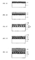
- One production method for a group III nitride crystal according to the present invention comprises the step of growing a group III nitride crystal film 2 on a substrate 1 as shown in Fig. 1A, the step of depositing a metallic film 3 on the group III nitride crystal film 2 as shown in Fig. 1B, the step of obtaining a group III nitride crystal portion 2a in which, not only a pore 4h is generated in the metallic layer, but also a void portion 2b is formed in the group III nitride crystal film 2 by thermally treating the substrate on which the group III nitride crystal film is grown and the metallic film is deposited as shown in Fig.
- the thermal treatment is satisfactory provided that it is performed at a temperature necessary for forming the void portion in the group III nitride film. Under these circumstances, it is preferable that the temperature of the thermal treatment be 700°C or more.
- the atmosphere at the time of growing the group III nitride crystal 5 for filling in the void portion 2b and growing the group III nitride crystal 6 on the metallic film in which the pore 4h is generated as an oxygen concentration of 0.1% by mol or less
- a wide range of group III nitride crystals including not only a GaN crystal, but also an Al x Ga y In 1-x-y N crystal can favorably be grown.
- the oxygen concentration is over 0.1% by mol, a dislocation density becomes large and an oxide may be generated or a spot defect to be caused by mixing of an oxygen ion may be generated thus inhibiting a favorable growth of the group III nitride crystal.
- the oxygen concentration is more preferably 0.01% by mol or less.
- Another production method for the group III nitride crystal according to the present invention comprises the step of growing the group III nitride crystal film 2 on the substrate 1 as shown in Fig. 1A, the step of depositing the metallic film 3 on the group III nitride crystal film 2 as shown in Fig. 1B, the step of not only changing the metallic film 3 into a metallic nitride film 4 and generating the pore 4h in the metallic nitride film 4, but also forming the void portion 2b in the group III nitride crystal film 2 by thermally treating the substrate on which the group III nitride crystal film 2 is grown and the metallic film is deposited as shown in Fig.
- At least a surface of the metallic film 3 is ordinarily nitrided to form the metallic nitride film 4 and, in order to promote nitriding of the metallic film, it is preferable that an N 2 gas or a gas containing a nitrogen atom (for example, NH 3 gas) be added as a nitrogen source at the time of the thermal treatment.
- an N 2 gas or a gas containing a nitrogen atom for example, NH 3 gas
- the thermal treatment even when the surface of the metallic film 3 is not nitrided, provided that at least the pore 4h is formed in the metallic film 3 and, further, the void portion 2b is formed in the group III nitride crystal film 2, at the time of forming the group III nitride crystal in an atmosphere of an oxygen concentration of 0.1% by mol or less, the group III nitride crystal is preferentially grown in the void portion 2b through the pore generated in the metallic film as the group III nitride crystal 5 for filling, to thereby fill the void portion 2b; therefore, the strain caused by the difference in the lattice constant between the substrate 1 and the group III nitride crystal 6 can be eliminated.
- a reducing atmosphere of an oxygen concentration of 0.1% by mol or less is formed as an atmosphere at the time of growing the group III nitride crystal for filling and the group III nitride crystal.
- the method of forming the atmosphere of an oxygen concentration of 0.1% by mol or less is not particularly limited provided that it does not go counter to the object of the present invention.
- a method in which, in addition to the N 2 gas or the NH 3 gas being used as a nitrogen source, and the H 2 gas being used as an oxygen reducing agent, a method using carbon or the like is mentioned as a favorable method. It is also favorable to use these methods simultaneously.
- a molar ratio of the H 2 gas to the NH 3 gas is preferably 10% or more. When the molar ratio is less than 10%, it is considered that an oxygen reduction effect is reduced.
- carbon (C) activated carbon, a carbon plate made of carbon, or the like is favorably used.
- carbon it is preferable to use carbon having a surface area (hereinafter, referred to also as "unit surface area"), based on 1 m 3 of an entire raw material gas, of 100 cm 2 /m 3 or more.
- an Al x Ga y In 1-x-y N crystal is preferable.
- the Al x Ga y In 1-x-y N crystal is extremely useful as a material for an LED or LD.
- titanium, vanadium or an alloy comprising at least one of titanium and vanadium is favorably mentioned.
- Metals or alloys other than these metals or the alloy can be used provided that they have a catalytic action of promoting decomposition of the group III nitride crystal film.
- Fe, Ni, Zr, Hf, W, Pt or an alloy comprising at least one metal element of these metals can be mentioned.
- the thickness of the metallic film is preferably from 10 nm to 1000 nm. In a case in which the thickness is less than 10 nm, when nitriding is performed, even when it is over 1000 nm the metallic film is liable to be peeled off, and it is difficult to generate the pore. Still further, in view of generating a stable pore, the thickness of the metallic film is more preferably from 20 nm to 500 nm.
- only the group III nitride crystal grown on the metallic film on the substrate can be obtained by removing the substrate.
- a method of removing the substrate is not particularly limited, and a method of removing the substrate by grinding or laser irradiation while the substrate is held, a method of separating the substrate having a different thermal expansion coefficient from the group III nitride crystal film by heat shock or the like can favorably be used.
- Still another production method for the group III nitride crystal according to the present invention comprises the step of further growing a group III nitride crystal on the group III nitride crystal obtained by the aforementioned production method for the group III nitride crystal in an atmosphere of an oxygen concentration of 0.1% by mol or less.
- the production method for the group III nitride crystal according to the present invention can be applied to multiple-stage growth of the group III nitride crystal, and allows the thickness of a layer of the group III nitride crystal having a small dislocation density to be large or allows the layers of two types or more of the group III nitride crystals each having a small dislocation density to be formed.
- the group III nitride crystal according to the present invention can be obtained by the aforementioned production method.
- the production method not only can the strain caused by the difference in the lattice constant between the substrate and the group III nitride crystal be eliminated, but also the oxygen concentration at the time of growing the group III nitride crystal be maintained at such a low concentration as 0.1% by mol or less and, accordingly the group III nitride crystal having a small dislocation density and good quality can be obtained.
- a 200 nm AIN crystal film which is a group III nitride crystal film 2 was grown on a sapphire substrate which is a substrate 1 by using an MOCVD method.
- trimethyl aluminum and NH 3 were used as a group III raw material and a nitrogen raw material, respectively.
- 100 nm of a Ti film was deposited as a metallic film 3 on the AIN crystal film which is a group III nitride crystal film 2 by an evaporation method. Subsequently, as shown in Fig.
- the resultant article was thermally treated for 30 minutes at 1000°C in an atmosphere of NH 3 gas in an oven (in Example 1, HVPE oven) for growing the crystal of the group III nitride crystal.
- a pore 4h was formed in the metallic film 3 while a void portion 2b was formed in the AIN crystal film which is the group III nitride crystal film 2.
- XRD X-ray Diffraction
- an AIN crystal which is each of a group III nitride crystal 5 for filling and a group III nitride crystal 6 was grown by using Al and NH 3 as a group III raw material and a nitrogen raw material, respectively, by using a Hydride Vapor Phase Epitaxy (hereinafter, referred to also as "HVPE") method.
- HVPE Hydride Vapor Phase Epitaxy
- an HCl gas was used as a carrier gas for Al; 40% of an H 2 gas based on the NH 3 gas which is a nitrogen raw material gas was used as an oxygen reducing agent; and a plate made of carbon having a unit surface area of 200 cm 2 /m 3 was used.
- a group III nitride crystal was prepared in the same manner as in Example 1 under the conditions shown in Table I or II, and then, was subjected to measurements of an FWHM value by XRD and a dislocation density. The results are collectively shown in Table I or II.
- AIN crystal was grown at an ambient temperature of 500°C and, subsequently, 100 ⁇ m of an AIN crystal was grown at an ambient temperature of 1000°C on a sapphire substrate by using an HVPE method.
- Al and NH 3 were used as a group III raw material and a nitrogen raw material, respectively.
- 50% of an H 2 gas based on a NH 3 gas which is a nitrogen raw material gas was used as an oxygen reducing agent and a plate made of carbon having a unit surface area of 1000 cm 2 /m 3 was used.
- the resultant AIN crystal showed an FWHM value of 220 arsec by XRD and a dislocation density of 8x10 9 cm -2 by TEM observation.
- Example 2 After an Al crystal film and a Ti film were formed on a sapphire substrate in the same manner as in Example 1, the resultant article was thermally treated. Thereafter, an AIN crystal was grown thereon by using an HVPE method. On this occasion, Al, an NH 3 gas and an HCl gas were used as a group III raw material, a nitrogen raw material and a carrier gas for Al, respectively. However, an oxygen reducing agent such as an H 2 gas or carbon was not used and the oxygen concentration was 0.5%. On this occasion, the AIN crystal was not obtained.
- the group III nitride crystal film and the metallic film were formed on the substrate, and then, after the resultant article was thermally treated, by forming an atmosphere of an oxygen concentration of 0.1% by mol or less when a group III nitride crystal for filling and a group III nitride crystal were grown, the group III nitride crystal having a dislocation density of less than 1x10 9 cm -2 and good quality was obtained. Further, by forming an atmosphere of an oxygen concentration of 0.01% by mol or less, a group III nitride crystal having a dislocation density of 1x10 8 cm -2 and good quality was obtained.
- Comparative Example 1 forms the group III nitride crystal film and the metallic film but does not comprise the step of the thermal treatment, the dislocation density became as large as 8x10 9 cm -2 , and, in Comparative Example 2, since the oxygen concentration at the time of forming the group III nitride crystal for filling and a group III nitride crystal became over 0.1% by mol, the AIN crystal which is a group III nitride crystal was not obtained.
- Example 7 by growing a group III nitride crystal on the group III nitride crystal by the production method according to the present invention, the group III nitride crystal having a dislocation density of less than 1x10 8 cm -2 and good quality was obtained.
- a group III nitride crystal film and a metallic film on a substrate, and then, after the resultant article is thermally treated, forming an atmosphere of an oxygen concentration of 0.1% by mol or less when a group III nitride crystal for filling and a group III nitride crystal were grown, not only a GaN crystal, but also a group III nitride crystal having a small dislocation density and good quality and a production method therefor can be provided.
Landscapes
- Chemical & Material Sciences (AREA)
- Engineering & Computer Science (AREA)
- Crystallography & Structural Chemistry (AREA)
- Materials Engineering (AREA)
- Metallurgy (AREA)
- Organic Chemistry (AREA)
- Inorganic Chemistry (AREA)
- Chemical Kinetics & Catalysis (AREA)
- General Chemical & Material Sciences (AREA)
- Crystals, And After-Treatments Of Crystals (AREA)
- Led Devices (AREA)
- Recrystallisation Techniques (AREA)
Abstract
A group III nitride crystal having a small dislocation density and good quality and a production method for the group III nitride crystal are provided. The production method for the group III nitride crystal is characterized by growing a group III nitride crystal film 2 on a substrate 1, depositing a metallic film 3 thereon and, then, not only changing the metallic film 3 into a metallic nitride film 4 and, further, generating a pore 4h, but also forming a void portion 2b in the group III nitride crystal film 2 by performing a thermal treatment and, thereafter, filling the void portion 2b by a group III nitride crystal 5 for filling by further growing a group III nitride crystal and, subsequently, growing a group III nitride crystal 6 on the metallic nitride film 4. <IMAGE>
Description
The present invention relates to a group III nitride crystal and a
production method for the group III nitride crystal and, particularly, to a group
III nitride having a low dislocation density and good quality, and a production
method for the group III nitride crystal.
A group III nitride crystal such as AlxGayIn1-x-yN crystal (0≤x, 0≤y,
x+y≤1) appears in the limelight as a material for a Light Emitting Diode
(hereinafter, referred to as "LED") or a Laser Diode (hereinafter, referred to
as "LD") and is expected to be deployed as an electronic device element.
However, it is difficult to grow the group III nitride crystal in bulk
crystal growth and, accordingly, a self-supporting substrate of the group III
nitride crystal has not been obtained. A substrate of the group III nitride
crystal which is presently in practical use is a sapphire substrate and a method
in which the group III nitride crystal is epitaxially grown on a single crystal
sapphire substrate by, for example, a Metalorganic Vapor Phase Epitaxy
(hereinafter, referred to as "MOVPE") method has ordinarily been employed.
Meanwhile, since the sapphire substrate is different in a lattice
constant from the AlxGayIn1-x-yN crystal, even when the AlxGayIn1-x-yN crystal is
grown directly on the sapphire substrate, a single crystal can not be obtained.
Thus, a method in which, firstly, a buffer layer of the AlxGayIn1-x-yN
crystal is grown on the sapphire substrate at a low temperature and, then, the
AlxGayIn1-x-yN crystal is then grown on the buffer layer has been proposed
(refer to, for example, JP-A No. 63-188983). By providing such buffer layer, a
strain between a lattice of the substrate and that of the AlxGayIn1-x-yN crystal
was relaxed, to thereby realize an epitaxial growth of the AlxGayIn1-x-yN single
crystal. However, even in such method, by a strain between the substrate and
the lattice of the AlxGayIn1-x-yN crystal, a dislocation of from 109 to 1010 cm-2 is
generated, to thereby cause a problem in preparing the LD or the like.
In order to reduce a dislocation density, a method in which a GaN layer
is grown on the sapphire substrate and, thereafter, a metallic layer is deposited
on the thus-grown GaN layer and, subsequently, the resultant article is
thermally treated to form a void portion in the GaN layer which is then filled by
performing the GaN crystal growth and, thereafter, the GaN crystal is grown
on the metallic layer has been proposed (refer to, for example, JP-A No.
2002-343728).
At present growth of group III nitride crystals other than a GaN crystal
has not been conducted by the aforementioned method.
Under these circumstances, an object of the present invention is to
provide not only the GaN crystal but also a group III nitride crystal having a
small dislocation density and good quality and a production method for these
crystals.
In order to attain the aforementioned object, a production method for a
group III nitride crystal according to the present invention is characterized by
comprising the steps of:
Further, a production method for a group III nitride crystal according to
the present invention is characterized by comprising the steps of:
Further, a group III nitride crystal according to the present invention is
obtained by the aforementioned method for obtaining the group III nitride
crystal.
One production method for a group III nitride crystal according to the
present invention, in reference to Fig. 1, comprises the step of growing a group
III nitride crystal film 2 on a substrate 1 as shown in Fig. 1A, the step of
depositing a metallic film 3 on the group III nitride crystal film 2 as shown in
Fig. 1B, the step of obtaining a group III nitride crystal portion 2a in which, not
only a pore 4h is generated in the metallic layer, but also a void portion 2b is
formed in the group III nitride crystal film 2 by thermally treating the
substrate on which the group III nitride crystal film is grown and the metallic
film is deposited as shown in Fig. 1C, the step of filling the void portion in the
group III nitride crystal film 2 by growing a group III nitride crystal 5 for filling
(the group III nitride crystal grown for the purpose of filling the void portion in
the group III nitride crystal film) on the group III nitride crystal portion 2a in
which the void portion 2b is formed in an atmosphere of an oxygen
concentration of 0.1% by mol or less as shown in Fig. 1D, and the step of
growing a group III nitride crystal 6 on the metallic film in an atmosphere of an
oxygen concentration of 0.1% by mol or less as shown in Fig. 1E.
By growing the group III nitride crystal 5 for filling in the void portion
2b in the group III nitride crystal film 2 generated by performing a thermal
treatment after the group III nitride crystal film 2 and the metallic film 3 are
formed to fill the void portion 2b and, further, growing the group III nitride
crystal 6 on the metallic film in which the pore 4h is generated by the thermal
treatment, a strain caused by a difference in a lattice constant between the
substrate 1 and the group III nitride crystal 6 can be eliminated. Therefore,
the thermal treatment is satisfactory provided that it is performed at a
temperature necessary for forming the void portion in the group III nitride film.
Under these circumstances, it is preferable that the temperature of the thermal
treatment be 700°C or more.
Further, by defining the atmosphere at the time of growing the group
III nitride crystal 5 for filling in the void portion 2b and growing the group III
nitride crystal 6 on the metallic film in which the pore 4h is generated as an
oxygen concentration of 0.1% by mol or less, a wide range of group III nitride
crystals including not only a GaN crystal, but also an AlxGayIn1-x-yN crystal can
favorably be grown. When the oxygen concentration is over 0.1% by mol, a
dislocation density becomes large and an oxide may be generated or a spot
defect to be caused by mixing of an oxygen ion may be generated thus
inhibiting a favorable growth of the group III nitride crystal. From the
standpoint of allowing the dislocation density to be small, the oxygen
concentration is more preferably 0.01% by mol or less.
Another production method for the group III nitride crystal according to
the present invention, in reference to Fig. 1, comprises the step of growing the
group III nitride crystal film 2 on the substrate 1 as shown in Fig. 1A, the step
of depositing the metallic film 3 on the group III nitride crystal film 2 as shown
in Fig. 1B, the step of not only changing the metallic film 3 into a metallic
nitride film 4 and generating the pore 4h in the metallic nitride film 4, but also
forming the void portion 2b in the group III nitride crystal film 2 by thermally
treating the substrate on which the group III nitride crystal film 2 is grown and
the metallic film is deposited as shown in Fig. 1C, the step of filling the void
portion in the group III nitride crystal film 2 by growing the group III nitride
crystal 5 for filling on the group III nitride crystal film 2 in which the void
portion 2b is formed in an atmosphere of an oxygen concentration of 0.1% by
mol or less as shown in Fig. 1D, and the step of growing the group III nitride
crystal 6 on the metallic nitride film 4 in an atmosphere of an oxygen
concentration of 0.1% by mol or less as shown in Fig. 1E.
By performing a thermal treatment after the group III nitride crystal
film 2 and the metallic film 3 are formed, at least a surface of the metallic film
3 is ordinarily nitrided to form the metallic nitride film 4 and, in order to
promote nitriding of the metallic film, it is preferable that an N2 gas or a gas
containing a nitrogen atom (for example, NH3 gas) be added as a nitrogen
source at the time of the thermal treatment. In such a manner of generating
the metallic nitride, forming of the pore 4h is promoted to facilitate the growth
of the group III nitride crystal 5 for filling in the void portion 2b.
On the other hand, by performing the thermal treatment, even when
the surface of the metallic film 3 is not nitrided, provided that at least the pore
4h is formed in the metallic film 3 and, further, the void portion 2b is formed in
the group III nitride crystal film 2, at the time of forming the group III nitride
crystal in an atmosphere of an oxygen concentration of 0.1% by mol or less, the
group III nitride crystal is preferentially grown in the void portion 2b through
the pore generated in the metallic film as the group III nitride crystal 5 for
filling, to thereby fill the void portion 2b; therefore, the strain caused by the
difference in the lattice constant between the substrate 1 and the group III
nitride crystal 6 can be eliminated. On this occasion, according to the present
invention, a reducing atmosphere of an oxygen concentration of 0.1% by mol or
less is formed as an atmosphere at the time of growing the group III nitride
crystal for filling and the group III nitride crystal. The method of forming the
atmosphere of an oxygen concentration of 0.1% by mol or less is not particularly
limited provided that it does not go counter to the object of the present
invention. For example, a method in which, in addition to the N2 gas or the
NH3 gas being used as a nitrogen source, and the H2 gas being used as an
oxygen reducing agent, a method using carbon or the like is mentioned as a
favorable method. It is also favorable to use these methods simultaneously.
On this occasion, when the H2 gas which is an oxygen reducing gas and the NH3
gas which is a nitrogen raw material gas are concurrently present, it is
considered that oxygen is removed by a reaction represented by the formula (1)
to be described below. In such case as described above, a molar ratio of the H2
gas to the NH3 gas is preferably 10% or more. When the molar ratio is less
than 10%, it is considered that an oxygen reduction effect is reduced.
3H2+2NH3+O2 → 2NH4+2H2O
As for carbon (C), activated carbon, a carbon plate made of carbon, or
the like is favorably used. When carbon is used, it is preferable to use carbon
having a surface area (hereinafter, referred to also as "unit surface area"),
based on 1 m3 of an entire raw material gas, of 100 cm2/m3 or more.
In the production method for the group III nitride crystal according to
the present invention, as for group iII nitride crystals, an AlxGayIn1-x-yN crystal
is preferable. In the group III nitride crystal, the AlxGayIn1-x-yN crystal is
extremely useful as a material for an LED or LD.
In the production method for the group III nitride crystal according to
the present invention, as for metallic films, titanium, vanadium or an alloy
comprising at least one of titanium and vanadium is favorably mentioned.
Metals or alloys other than these metals or the alloy can be used provided that
they have a catalytic action of promoting decomposition of the group III nitride
crystal film. For example, Fe, Ni, Zr, Hf, W, Pt or an alloy comprising at least
one metal element of these metals can be mentioned.
Further, the thickness of the metallic film is preferably from 10 nm to
1000 nm. In a case in which the thickness is less than 10 nm, when nitriding
is performed, even when it is over 1000 nm the metallic film is liable to be
peeled off, and it is difficult to generate the pore. Still further, in view of
generating a stable pore, the thickness of the metallic film is more preferably
from 20 nm to 500 nm.
Further, in the production method for the group III nitride crystal
according to the present invention, only the group III nitride crystal grown on
the metallic film on the substrate can be obtained by removing the substrate.
A method of removing the substrate is not particularly limited, and a method of
removing the substrate by grinding or laser irradiation while the substrate is
held, a method of separating the substrate having a different thermal
expansion coefficient from the group III nitride crystal film by heat shock or the
like can favorably be used.
Further, still another production method for the group III nitride
crystal according to the present invention comprises the step of further growing
a group III nitride crystal on the group III nitride crystal obtained by the
aforementioned production method for the group III nitride crystal in an
atmosphere of an oxygen concentration of 0.1% by mol or less. The production
method for the group III nitride crystal according to the present invention can
be applied to multiple-stage growth of the group III nitride crystal, and allows
the thickness of a layer of the group III nitride crystal having a small
dislocation density to be large or allows the layers of two types or more of the
group III nitride crystals each having a small dislocation density to be formed.
The group III nitride crystal according to the present invention can be
obtained by the aforementioned production method. By the production
method, not only can the strain caused by the difference in the lattice constant
between the substrate and the group III nitride crystal be eliminated, but also
the oxygen concentration at the time of growing the group III nitride crystal be
maintained at such a low concentration as 0.1% by mol or less and, accordingly
the group III nitride crystal having a small dislocation density and good quality
can be obtained.
Hereinafter, the present invention will more specifically be described
with reference to the embodiments.
In reference to Fig. 1, as shown in Fig. 1A, a 200 nm AIN crystal film
which is a group III nitride crystal film 2 was grown on a sapphire substrate
which is a substrate 1 by using an MOCVD method. On this occasion,
trimethyl aluminum and NH3 were used as a group III raw material and a
nitrogen raw material, respectively. Next, as shown in Fig. 1B, 100 nm of a Ti
film was deposited as a metallic film 3 on the AIN crystal film which is a group
III nitride crystal film 2 by an evaporation method. Subsequently, as shown in
Fig. 1C, the resultant article was thermally treated for 30 minutes at 1000°C in
an atmosphere of NH3 gas in an oven (in Example 1, HVPE oven) for growing
the crystal of the group III nitride crystal. By such thermal treatment as
described above, a pore 4h was formed in the metallic film 3 while a void
portion 2b was formed in the AIN crystal film which is the group III nitride
crystal film 2. When the surface of the metallic film was analyzed by X-ray
Diffraction (hereinafter, referred to also as "XRD"), it was found that the TiN
film was formed.
Thereafter, as shown in Figs. 1D and 1E, an AIN crystal which is each
of a group III nitride crystal 5 for filling and a group III nitride crystal 6 was
grown by using Al and NH3 as a group III raw material and a nitrogen raw
material, respectively, by using a Hydride Vapor Phase Epitaxy (hereinafter,
referred to also as "HVPE") method. On this occasion, an HCl gas was used as
a carrier gas for Al; 40% of an H2 gas based on the NH3 gas which is a nitrogen
raw material gas was used as an oxygen reducing agent; and a plate made of
carbon having a unit surface area of 200 cm2/m3 was used. Growth of the AIN
crystal by the HVPE method first appeared preferentially in the void portion 2b
of the AIN crystal film passing through the pore 4h in the metallic film, to
thereby fill the void portion 2b. Thereafter, 400 µm of an AIN crystal which is
the group III nitride crystal 6 was grown on a Ti film on a surface of which the
TiN film which is the metallic nitride film 4 was formed. The resultant AIN
crystal showed a Full Width Half Maximum (hereinafter, referred to also as
"FWHM") value of 90 arsec by XRD and a dislocation density of 6x107 cm-2 by
TEM observation. The results are collectively shown in Table I.
A group III nitride crystal was prepared in the same manner as in
Example 1 under the conditions shown in Table I or II, and then, was subjected
to measurements of an FWHM value by XRD and a dislocation density. The
results are collectively shown in Table I or II.


Firstly, 10 nm of a buffer layer of AIN was grown at an ambient
temperature of 500°C and, subsequently, 100 µm of an AIN crystal was grown
at an ambient temperature of 1000°C on a sapphire substrate by using an
HVPE method. On this occasion, Al and NH3 were used as a group III raw
material and a nitrogen raw material, respectively. Further, 50% of an H2 gas
based on a NH3 gas which is a nitrogen raw material gas was used as an oxygen
reducing agent and a plate made of carbon having a unit surface area of 1000
cm2/m3 was used. The resultant AIN crystal showed an FWHM value of 220
arsec by XRD and a dislocation density of 8x109 cm-2 by TEM observation.
After an Al crystal film and a Ti film were formed on a sapphire
substrate in the same manner as in Example 1, the resultant article was
thermally treated. Thereafter, an AIN crystal was grown thereon by using an
HVPE method. On this occasion, Al, an NH3 gas and an HCl gas were used as
a group III raw material, a nitrogen raw material and a carrier gas for Al,
respectively. However, an oxygen reducing agent such as an H2 gas or carbon
was not used and the oxygen concentration was 0.5%. On this occasion, the
AIN crystal was not obtained.
500 µm of a Al0.4Ga0.6N crystal was further grown on the Al0.4Ga0.6N
crystal obtained in Example 4 in an atmosphere of an oxygen concentration of
0.02% by mol by using 40% by mol of Al and 60% by mol of Ga as group III raw
materials and an NH3 gas as a nitrogen raw material by means of an HVPE
method. On this occasion, an HCl gas was used as a carrier gas for each Al
and Ga and 30% of an H2 gas based on the NH3 gas which is a nitrogen raw
material gas was used. The Al0.4Ga0.6N crystal obtained in the present
Example showed an FWHM value of 82 arsec by XRD and a dislocation value of
8x106 cm-2 by TEM observation.
As shown in Examples 1 to 6 in Tables I and II, the group III nitride
crystal film and the metallic film were formed on the substrate, and then, after
the resultant article was thermally treated, by forming an atmosphere of an
oxygen concentration of 0.1% by mol or less when a group III nitride crystal for
filling and a group III nitride crystal were grown, the group III nitride crystal
having a dislocation density of less than 1x109 cm-2 and good quality was
obtained. Further, by forming an atmosphere of an oxygen concentration of
0.01% by mol or less, a group III nitride crystal having a dislocation density of
1x108 cm-2 and good quality was obtained.
In contrast, since Comparative Example 1 forms the group III nitride
crystal film and the metallic film but does not comprise the step of the thermal
treatment, the dislocation density became as large as 8x109 cm-2, and, in
Comparative Example 2, since the oxygen concentration at the time of forming
the group III nitride crystal for filling and a group III nitride crystal became
over 0.1% by mol, the AIN crystal which is a group III nitride crystal was not
obtained.
Further, as shown in Example 7, by growing a group III nitride crystal
on the group III nitride crystal by the production method according to the
present invention, the group III nitride crystal having a dislocation density of
less than 1x108 cm-2 and good quality was obtained.
It is to be understood that embodiments and examples disclosed herein
are illustrative and not restrictive in all aspects. The scope of the invention
should be determined with reference to the appended claims and not to the
above descriptions and is intended to include meanings equivalent to such
claims and all such modifications and variations as fall within the scope of such
claims.
As has been described above, according to the present invention, by
forming a group III nitride crystal film and a metallic film on a substrate, and
then, after the resultant article is thermally treated, forming an atmosphere of
an oxygen concentration of 0.1% by mol or less when a group III nitride crystal
for filling and a group III nitride crystal were grown, not only a GaN crystal,
but also a group III nitride crystal having a small dislocation density and good
quality and a production method therefor can be provided.
Claims (9)
- A production method for a group III nitride crystal, being
characterized by comprising the steps of:growing a group III nitride crystal film on a substrate;depositing a metallic film on the group III nitride crystal film;not only generating a pore in the metallic film but also forming a void portion in the group III nitride crystal film by thermally treating the substrate on which the group III nitride crystal film is grown and the metallic film is deposited;growing a group III nitride crystal for filling on the group III nitride crystal film in which the void portion is formed in an atmosphere of an oxygen concentration of 0.1% by mol or less to fill the void portion in the group III nitride crystal film; andgrowing a group III nitride crystal on the metallic film in an atmosphere of an oxygen concentration of 0.1% by mol or less. - A production method for a group III nitride crystal, being characterized by comprising the steps of:growing a group III nitride crystal film on a substrate;depositing a metallic film on the group III nitride crystal film;not only changing the metallic film into a metallic nitride film and, further, generating a pore in the metallic film, but also forming a void portion in the group III nitride crystal film by thermally treating the substrate on which the group III nitride crystal film is grown and the metallic film is deposited;growing a group III nitride crystal for filling on the group III nitride crystal film in which the void portion is formed in an atmosphere of an oxygen concentration of 0.1% by mol or less to fill the void portion in the group III nitride crystal film; andgrowing a group III nitride crystal on the metallic nitride film in an atmosphere of an oxygen concentration of 0.1% by mol or less.
- The production method for the group III nitride crystal as set forth in Claim 1 or 2, being characterized by forming the atmosphere of an oxygen concentration of 0.1% by mol or less at the time of growing the group III nitride crystal for filling and/or the group III nitride crystal, by at least one of a method of using an H2 gas and a method of using carbon.
- The production method for the group III nitride crystal as set forth in any one of Claims 1 to 3, wherein the group III nitride crystal is an AlxGayIn1-x-yN crystal (0≤x, 0≤y, x+y≤1).
- The production method for the group III nitride crystal as set forth in any one of Claims 1 to 4, wherein the metallic film comprises titanium, vanadium or an alloy comprising at least one of titanium and vanadium.
- The production method for the group III nitride crystal as set forth in any one of Claims 1 to 5, wherein thickness of the metallic film is from 10 nm to 1000 nm.
- The production method for the group III nitride crystal as set forth in any one of Claims 1 to 6, being characterized by further removing the substrate to obtain only the group III nitride crystal grown on the metallic film of the substrate.
- A production method for a group III nitride crystal, being
characterized by further comprising the step of growing a group III nitride crystal in an oxygen atmosphere of 0.1% by mol or less on the group III nitride crystal obtained by the method as set forth in any one of Claims 1 to 7. - A group III nitride crystal, being obtained by the method for obtaining the group III nitride crystal as set forth in any one of Claims 1 to 8.
Applications Claiming Priority (3)
| Application Number | Priority Date | Filing Date | Title |
|---|---|---|---|
| JP2003165083A JP2005005378A (en) | 2003-06-10 | 2003-06-10 | Group III nitride crystal and method for producing the same |
| JP2003165083 | 2003-06-10 | ||
| PCT/JP2004/007420 WO2004112112A1 (en) | 2003-06-10 | 2004-05-24 | Iii nitride crystal and method for producing same |
Publications (1)
| Publication Number | Publication Date |
|---|---|
| EP1523033A1 true EP1523033A1 (en) | 2005-04-13 |
Family
ID=33549200
Family Applications (1)
| Application Number | Title | Priority Date | Filing Date |
|---|---|---|---|
| EP04734604A Withdrawn EP1523033A1 (en) | 2003-06-10 | 2004-05-24 | Group iii nitride crystal and method for producing same |
Country Status (6)
| Country | Link |
|---|---|
| US (1) | US20050257733A1 (en) |
| EP (1) | EP1523033A1 (en) |
| JP (1) | JP2005005378A (en) |
| CN (1) | CN1701415A (en) |
| TW (1) | TW200509225A (en) |
| WO (1) | WO2004112112A1 (en) |
Cited By (2)
| Publication number | Priority date | Publication date | Assignee | Title |
|---|---|---|---|---|
| EP2378545A4 (en) * | 2008-12-26 | 2013-07-10 | Dowa Holdings Co Ltd | NITRIDE III SEMICONDUCTOR GROWTH SUBSTRATE, NITRIDE III SEMICONDUCTOR EPITAXIAL SUBSTRATE, NITRIDE III SEMICONDUCTOR ELEMENT, NITRIDE III SEMICONDUCTOR SELF-CARRIER SUBSTRATE, AND METHOD OF MANUFACTURING THE SAME |
| EP2031642A3 (en) * | 2007-08-28 | 2014-07-02 | DOWA Electronics Materials Co., Ltd. | Group III nitride semiconductor and a manufacturing method thereof |
Families Citing this family (14)
| Publication number | Priority date | Publication date | Assignee | Title |
|---|---|---|---|---|
| JP4932121B2 (en) * | 2002-03-26 | 2012-05-16 | 日本電気株式会社 | Method for manufacturing group III-V nitride semiconductor substrate |
| JP2007042843A (en) * | 2005-08-03 | 2007-02-15 | Furukawa Co Ltd | Al-containing nitride hydride vapor phase growth apparatus, Al-containing nitride semiconductor substrate manufacturing method, and Al-containing nitride semiconductor substrate |
| JP5005266B2 (en) * | 2006-03-02 | 2012-08-22 | 日本碍子株式会社 | AlN crystal fabrication method and AlN thick film |
| WO2007122669A1 (en) * | 2006-03-29 | 2007-11-01 | Fujitsu Limited | COMPOUND SEMICONDUCTOR WAFER HAVING POLYCRYSTALLINE SiC SUBSTRATE, COMPOUND SEMICONDUCTOR DEVICE, AND PROCESSES FOR PRODUCING THESE |
| US7879697B2 (en) | 2006-06-05 | 2011-02-01 | Regents Of The University Of Minnesota | Growth of low dislocation density Group-III nitrides and related thin-film structures |
| EP2039812A4 (en) * | 2006-06-20 | 2010-08-11 | Sumitomo Electric Industries | PROCESS FOR GROWING A CRYSTAL OF AlxGa1-xN, AND CRYSTAL SUBSTRATE OF AlxGa1-xN |
| EP2243866A1 (en) * | 2008-01-16 | 2010-10-27 | National University Corporation Tokyo University of Agriculture and Technology | Process for producing laminate comprising al-based group iii nitride single crystal layer, laminate produced by the process, process for producing al-based group iii nitride single crystal substrate using the laminate, and aluminum nitride single crystal substrate |
| JP4513927B1 (en) | 2009-09-30 | 2010-07-28 | 住友電気工業株式会社 | Group III nitride semiconductor substrate, epitaxial substrate, and semiconductor device |
| JP5365454B2 (en) | 2009-09-30 | 2013-12-11 | 住友電気工業株式会社 | Group III nitride semiconductor substrate, epitaxial substrate, and semiconductor device |
| CN103311391B (en) | 2012-03-06 | 2016-07-20 | 展晶科技(深圳)有限公司 | LED crystal particle and preparation method thereof |
| CN107275187B (en) * | 2017-06-26 | 2020-06-05 | 镓特半导体科技(上海)有限公司 | Self-supporting gallium nitride layer and preparation method and annealing method thereof |
| CN111128686A (en) * | 2019-12-30 | 2020-05-08 | 镓特半导体科技(上海)有限公司 | Semiconductor structure, self-supporting gallium nitride layer and preparation method thereof |
| JP7478826B2 (en) * | 2020-01-16 | 2024-05-07 | エスエルティー テクノロジーズ インコーポレイテッド | High quality group III metal nitride seed crystals and method for producing same - Patents.com |
| CN116024656B (en) * | 2022-12-08 | 2026-07-17 | 中国科学院苏州纳米技术与纳米仿生研究所 | Method for growing III-nitride film on SiC substrate and application thereof |
Family Cites Families (3)
| Publication number | Priority date | Publication date | Assignee | Title |
|---|---|---|---|---|
| JP3788104B2 (en) * | 1998-05-28 | 2006-06-21 | 住友電気工業株式会社 | Gallium nitride single crystal substrate and manufacturing method thereof |
| JP3631724B2 (en) * | 2001-03-27 | 2005-03-23 | 日本電気株式会社 | Group III nitride semiconductor substrate and manufacturing method thereof |
| JP3886341B2 (en) * | 2001-05-21 | 2007-02-28 | 日本電気株式会社 | Method for manufacturing gallium nitride crystal substrate and gallium nitride crystal substrate |
-
2003
- 2003-06-10 JP JP2003165083A patent/JP2005005378A/en not_active Withdrawn
-
2004
- 2004-05-24 US US10/524,271 patent/US20050257733A1/en not_active Abandoned
- 2004-05-24 EP EP04734604A patent/EP1523033A1/en not_active Withdrawn
- 2004-05-24 WO PCT/JP2004/007420 patent/WO2004112112A1/en not_active Ceased
- 2004-05-24 CN CNA2004800007999A patent/CN1701415A/en active Pending
- 2004-06-02 TW TW093115833A patent/TW200509225A/en unknown
Non-Patent Citations (1)
| Title |
|---|
| See references of WO2004112112A1 * |
Cited By (3)
| Publication number | Priority date | Publication date | Assignee | Title |
|---|---|---|---|---|
| EP2031642A3 (en) * | 2007-08-28 | 2014-07-02 | DOWA Electronics Materials Co., Ltd. | Group III nitride semiconductor and a manufacturing method thereof |
| EP2378545A4 (en) * | 2008-12-26 | 2013-07-10 | Dowa Holdings Co Ltd | NITRIDE III SEMICONDUCTOR GROWTH SUBSTRATE, NITRIDE III SEMICONDUCTOR EPITAXIAL SUBSTRATE, NITRIDE III SEMICONDUCTOR ELEMENT, NITRIDE III SEMICONDUCTOR SELF-CARRIER SUBSTRATE, AND METHOD OF MANUFACTURING THE SAME |
| US8736025B2 (en) | 2008-12-26 | 2014-05-27 | Dowa Electroncs Materials Co., Ltd. | III-nitride semiconductor growth substrate, III-nitride semiconductor epitaxial substrate, III-nitride semiconductor element, III-nitride semiconductor freestanding substrate all having improved crystallinity |
Also Published As
| Publication number | Publication date |
|---|---|
| US20050257733A1 (en) | 2005-11-24 |
| TW200509225A (en) | 2005-03-01 |
| WO2004112112A1 (en) | 2004-12-23 |
| JP2005005378A (en) | 2005-01-06 |
| CN1701415A (en) | 2005-11-23 |
Similar Documents
| Publication | Publication Date | Title |
|---|---|---|
| JP4824313B2 (en) | Process for obtaining a gallium-containing nitride bulk single crystal, a process for eliminating impurities from the obtained crystal, and a process for producing a substrate comprising a gallium-containing nitride bulk single crystal | |
| JP4117156B2 (en) | Method for manufacturing group III nitride semiconductor substrate | |
| US6924159B2 (en) | Semiconductor substrate made of group III nitride, and process for manufacture thereof | |
| US7410539B2 (en) | Template type substrate and a method of preparing the same | |
| AU2004276541B2 (en) | Method of producing self-supporting substrates comprising III-nitrides by means of heteroepitaxy on a sacrificial layer | |
| JP4396816B2 (en) | Group III nitride semiconductor substrate and manufacturing method thereof | |
| KR100718188B1 (en) | Non-polar single crystalline a-plane nitride semiconductor wafer and preparation thereof | |
| JP3886341B2 (en) | Method for manufacturing gallium nitride crystal substrate and gallium nitride crystal substrate | |
| US7621998B2 (en) | Single crystalline gallium nitride thick film having reduced bending deformation | |
| US20050257733A1 (en) | III nitride crystal and method for producing same | |
| TW201221708A (en) | Method for producing aluminum nitride crystals | |
| KR101503618B1 (en) | Method for producing substrate for group iii nitride semiconductor element fabrication, method for producing group iii nitride semiconductor free-standing substrate or group iii nitride semiconductor element, and group iii nitride growth substrate | |
| JP4838766B2 (en) | Group III nitride semiconductor substrate manufacturing method and group III nitride semiconductor substrate | |
| JP2010030877A (en) | Group iii nitride semiconductor substrate and method for producing the same | |
| JP5333374B2 (en) | GaN crystal manufacturing method, GaN crystal substrate, and group III nitride semiconductor device | |
| JP4340866B2 (en) | Nitride semiconductor substrate and manufacturing method thereof | |
| JP2011042542A (en) | Method for producing group iii nitride substrate, and group iii nitride substrate | |
| JP4825747B2 (en) | Method for producing nonpolar plane group III nitride single crystal | |
| JP2010222642A (en) | Method for manufacturing group III nitride semiconductor substrate | |
| JP7720900B2 (en) | Semiconductor substrate having a nitrided interface layer - Patents.com | |
| CN100472000C (en) | Manufacturing method of bulk single crystal gallium-containing nitride | |
| JP4885997B2 (en) | Method for manufacturing group III nitride semiconductor substrate | |
| KR101220826B1 (en) | Process for the preparation of single crystalline gallium nitride thick layer | |
| JP5441762B2 (en) | Manufacturing method of laminate | |
| JP3274676B2 (en) | Method for manufacturing gallium nitride-based compound semiconductor |
Legal Events
| Date | Code | Title | Description |
|---|---|---|---|
| PUAI | Public reference made under article 153(3) epc to a published international application that has entered the european phase |
Free format text: ORIGINAL CODE: 0009012 |
|
| 17P | Request for examination filed |
Effective date: 20050114 |
|
| AK | Designated contracting states |
Kind code of ref document: A1 Designated state(s): AT BE BG CH CY CZ DE DK EE ES FI FR GB GR HU IE IT LI LU MC NL PL PT RO SE SI SK TR |
|
| AX | Request for extension of the european patent |
Extension state: AL HR LT LV MK |
|
| STAA | Information on the status of an ep patent application or granted ep patent |
Free format text: STATUS: THE APPLICATION HAS BEEN WITHDRAWN |
|
| 18W | Application withdrawn |
Effective date: 20051031 |