EP1522612A1 - Iii-v compound semiconductor crystal and method for production thereof - Google Patents
Iii-v compound semiconductor crystal and method for production thereof Download PDFInfo
- Publication number
- EP1522612A1 EP1522612A1 EP04725190A EP04725190A EP1522612A1 EP 1522612 A1 EP1522612 A1 EP 1522612A1 EP 04725190 A EP04725190 A EP 04725190A EP 04725190 A EP04725190 A EP 04725190A EP 1522612 A1 EP1522612 A1 EP 1522612A1
- Authority
- EP
- European Patent Office
- Prior art keywords
- group iii
- crystal
- metal film
- substrate
- compound
- Prior art date
- Legal status (The legal status is an assumption and is not a legal conclusion. Google has not performed a legal analysis and makes no representation as to the accuracy of the status listed.)
- Withdrawn
Links
Images


Classifications
-
- H—ELECTRICITY
- H10—SEMICONDUCTOR DEVICES; ELECTRIC SOLID-STATE DEVICES NOT OTHERWISE PROVIDED FOR
- H10P—GENERIC PROCESSES OR APPARATUS FOR THE MANUFACTURE OR TREATMENT OF DEVICES COVERED BY CLASS H10
- H10P14/00—Formation of materials, e.g. in the shape of layers or pillars
- H10P14/20—Formation of materials, e.g. in the shape of layers or pillars of semiconductor materials
- H10P14/29—Formation of materials, e.g. in the shape of layers or pillars of semiconductor materials characterised by the substrates
- H10P14/2901—Materials
- H10P14/2902—Materials being Group IVA materials
- H10P14/2904—Silicon carbide
-
- C—CHEMISTRY; METALLURGY
- C30—CRYSTAL GROWTH
- C30B—SINGLE-CRYSTAL GROWTH; UNIDIRECTIONAL SOLIDIFICATION OF EUTECTIC MATERIAL OR UNIDIRECTIONAL DEMIXING OF EUTECTOID MATERIAL; REFINING BY ZONE-MELTING OF MATERIAL; PRODUCTION OF A HOMOGENEOUS POLYCRYSTALLINE MATERIAL WITH DEFINED STRUCTURE; SINGLE CRYSTALS OR HOMOGENEOUS POLYCRYSTALLINE MATERIAL WITH DEFINED STRUCTURE; AFTER-TREATMENT OF SINGLE CRYSTALS OR A HOMOGENEOUS POLYCRYSTALLINE MATERIAL WITH DEFINED STRUCTURE; APPARATUS THEREFOR
- C30B25/00—Single-crystal growth by chemical reaction of reactive gases, e.g. chemical vapour-deposition growth
- C30B25/02—Epitaxial-layer growth
-
- C—CHEMISTRY; METALLURGY
- C30—CRYSTAL GROWTH
- C30B—SINGLE-CRYSTAL GROWTH; UNIDIRECTIONAL SOLIDIFICATION OF EUTECTIC MATERIAL OR UNIDIRECTIONAL DEMIXING OF EUTECTOID MATERIAL; REFINING BY ZONE-MELTING OF MATERIAL; PRODUCTION OF A HOMOGENEOUS POLYCRYSTALLINE MATERIAL WITH DEFINED STRUCTURE; SINGLE CRYSTALS OR HOMOGENEOUS POLYCRYSTALLINE MATERIAL WITH DEFINED STRUCTURE; AFTER-TREATMENT OF SINGLE CRYSTALS OR A HOMOGENEOUS POLYCRYSTALLINE MATERIAL WITH DEFINED STRUCTURE; APPARATUS THEREFOR
- C30B25/00—Single-crystal growth by chemical reaction of reactive gases, e.g. chemical vapour-deposition growth
- C30B25/02—Epitaxial-layer growth
- C30B25/18—Epitaxial-layer growth characterised by the substrate
-
- C—CHEMISTRY; METALLURGY
- C30—CRYSTAL GROWTH
- C30B—SINGLE-CRYSTAL GROWTH; UNIDIRECTIONAL SOLIDIFICATION OF EUTECTIC MATERIAL OR UNIDIRECTIONAL DEMIXING OF EUTECTOID MATERIAL; REFINING BY ZONE-MELTING OF MATERIAL; PRODUCTION OF A HOMOGENEOUS POLYCRYSTALLINE MATERIAL WITH DEFINED STRUCTURE; SINGLE CRYSTALS OR HOMOGENEOUS POLYCRYSTALLINE MATERIAL WITH DEFINED STRUCTURE; AFTER-TREATMENT OF SINGLE CRYSTALS OR A HOMOGENEOUS POLYCRYSTALLINE MATERIAL WITH DEFINED STRUCTURE; APPARATUS THEREFOR
- C30B29/00—Single crystals or homogeneous polycrystalline material with defined structure characterised by the material or by their shape
- C30B29/10—Inorganic compounds or compositions
- C30B29/40—AIIIBV compounds wherein A is B, Al, Ga, In or Tl and B is N, P, As, Sb or Bi
-
- C—CHEMISTRY; METALLURGY
- C30—CRYSTAL GROWTH
- C30B—SINGLE-CRYSTAL GROWTH; UNIDIRECTIONAL SOLIDIFICATION OF EUTECTIC MATERIAL OR UNIDIRECTIONAL DEMIXING OF EUTECTOID MATERIAL; REFINING BY ZONE-MELTING OF MATERIAL; PRODUCTION OF A HOMOGENEOUS POLYCRYSTALLINE MATERIAL WITH DEFINED STRUCTURE; SINGLE CRYSTALS OR HOMOGENEOUS POLYCRYSTALLINE MATERIAL WITH DEFINED STRUCTURE; AFTER-TREATMENT OF SINGLE CRYSTALS OR A HOMOGENEOUS POLYCRYSTALLINE MATERIAL WITH DEFINED STRUCTURE; APPARATUS THEREFOR
- C30B29/00—Single crystals or homogeneous polycrystalline material with defined structure characterised by the material or by their shape
- C30B29/10—Inorganic compounds or compositions
- C30B29/40—AIIIBV compounds wherein A is B, Al, Ga, In or Tl and B is N, P, As, Sb or Bi
- C30B29/403—AIII-nitrides
-
- C—CHEMISTRY; METALLURGY
- C30—CRYSTAL GROWTH
- C30B—SINGLE-CRYSTAL GROWTH; UNIDIRECTIONAL SOLIDIFICATION OF EUTECTIC MATERIAL OR UNIDIRECTIONAL DEMIXING OF EUTECTOID MATERIAL; REFINING BY ZONE-MELTING OF MATERIAL; PRODUCTION OF A HOMOGENEOUS POLYCRYSTALLINE MATERIAL WITH DEFINED STRUCTURE; SINGLE CRYSTALS OR HOMOGENEOUS POLYCRYSTALLINE MATERIAL WITH DEFINED STRUCTURE; AFTER-TREATMENT OF SINGLE CRYSTALS OR A HOMOGENEOUS POLYCRYSTALLINE MATERIAL WITH DEFINED STRUCTURE; APPARATUS THEREFOR
- C30B29/00—Single crystals or homogeneous polycrystalline material with defined structure characterised by the material or by their shape
- C30B29/10—Inorganic compounds or compositions
- C30B29/40—AIIIBV compounds wherein A is B, Al, Ga, In or Tl and B is N, P, As, Sb or Bi
- C30B29/403—AIII-nitrides
- C30B29/406—Gallium nitride
-
- H—ELECTRICITY
- H01—ELECTRIC ELEMENTS
- H01S—DEVICES USING THE PROCESS OF LIGHT AMPLIFICATION BY STIMULATED EMISSION OF RADIATION [LASER] TO AMPLIFY OR GENERATE LIGHT; DEVICES USING STIMULATED EMISSION OF ELECTROMAGNETIC RADIATION IN WAVE RANGES OTHER THAN OPTICAL
- H01S5/00—Semiconductor lasers
- H01S5/30—Structure or shape of the active region; Materials used for the active region
- H01S5/32—Structure or shape of the active region; Materials used for the active region comprising PN junctions, e.g. hetero- or double- heterostructures
- H01S5/323—Structure or shape of the active region; Materials used for the active region comprising PN junctions, e.g. hetero- or double- heterostructures in AIIIBV compounds, e.g. AlGaAs-laser, InP-based laser
-
- H—ELECTRICITY
- H10—SEMICONDUCTOR DEVICES; ELECTRIC SOLID-STATE DEVICES NOT OTHERWISE PROVIDED FOR
- H10P—GENERIC PROCESSES OR APPARATUS FOR THE MANUFACTURE OR TREATMENT OF DEVICES COVERED BY CLASS H10
- H10P14/00—Formation of materials, e.g. in the shape of layers or pillars
- H10P14/20—Formation of materials, e.g. in the shape of layers or pillars of semiconductor materials
- H10P14/27—Formation of materials, e.g. in the shape of layers or pillars of semiconductor materials using selective deposition, e.g. simultaneous growth of monocrystalline and non-monocrystalline semiconductor materials
- H10P14/271—Formation of materials, e.g. in the shape of layers or pillars of semiconductor materials using selective deposition, e.g. simultaneous growth of monocrystalline and non-monocrystalline semiconductor materials characterised by the preparation of substrate for selective deposition
- H10P14/272—Formation of materials, e.g. in the shape of layers or pillars of semiconductor materials using selective deposition, e.g. simultaneous growth of monocrystalline and non-monocrystalline semiconductor materials characterised by the preparation of substrate for selective deposition using mask materials other than SiO2 or SiN
-
- H—ELECTRICITY
- H10—SEMICONDUCTOR DEVICES; ELECTRIC SOLID-STATE DEVICES NOT OTHERWISE PROVIDED FOR
- H10P—GENERIC PROCESSES OR APPARATUS FOR THE MANUFACTURE OR TREATMENT OF DEVICES COVERED BY CLASS H10
- H10P14/00—Formation of materials, e.g. in the shape of layers or pillars
- H10P14/20—Formation of materials, e.g. in the shape of layers or pillars of semiconductor materials
- H10P14/29—Formation of materials, e.g. in the shape of layers or pillars of semiconductor materials characterised by the substrates
- H10P14/2901—Materials
- H10P14/2902—Materials being Group IVA materials
- H10P14/2905—Silicon, silicon germanium or germanium
-
- H—ELECTRICITY
- H10—SEMICONDUCTOR DEVICES; ELECTRIC SOLID-STATE DEVICES NOT OTHERWISE PROVIDED FOR
- H10P—GENERIC PROCESSES OR APPARATUS FOR THE MANUFACTURE OR TREATMENT OF DEVICES COVERED BY CLASS H10
- H10P14/00—Formation of materials, e.g. in the shape of layers or pillars
- H10P14/20—Formation of materials, e.g. in the shape of layers or pillars of semiconductor materials
- H10P14/29—Formation of materials, e.g. in the shape of layers or pillars of semiconductor materials characterised by the substrates
- H10P14/2901—Materials
- H10P14/2921—Materials being crystalline insulating materials
-
- H—ELECTRICITY
- H10—SEMICONDUCTOR DEVICES; ELECTRIC SOLID-STATE DEVICES NOT OTHERWISE PROVIDED FOR
- H10P—GENERIC PROCESSES OR APPARATUS FOR THE MANUFACTURE OR TREATMENT OF DEVICES COVERED BY CLASS H10
- H10P14/00—Formation of materials, e.g. in the shape of layers or pillars
- H10P14/20—Formation of materials, e.g. in the shape of layers or pillars of semiconductor materials
- H10P14/34—Deposited materials, e.g. layers
- H10P14/3402—Deposited materials, e.g. layers characterised by the chemical composition
- H10P14/3414—Deposited materials, e.g. layers characterised by the chemical composition being group IIIA-VIA materials
-
- Y—GENERAL TAGGING OF NEW TECHNOLOGICAL DEVELOPMENTS; GENERAL TAGGING OF CROSS-SECTIONAL TECHNOLOGIES SPANNING OVER SEVERAL SECTIONS OF THE IPC; TECHNICAL SUBJECTS COVERED BY FORMER USPC CROSS-REFERENCE ART COLLECTIONS [XRACs] AND DIGESTS
- Y10—TECHNICAL SUBJECTS COVERED BY FORMER USPC
- Y10T—TECHNICAL SUBJECTS COVERED BY FORMER US CLASSIFICATION
- Y10T428/00—Stock material or miscellaneous articles
- Y10T428/12—All metal or with adjacent metals
- Y10T428/12493—Composite; i.e., plural, adjacent, spatially distinct metal components [e.g., layers, joint, etc.]
- Y10T428/12674—Ge- or Si-base component
-
- Y—GENERAL TAGGING OF NEW TECHNOLOGICAL DEVELOPMENTS; GENERAL TAGGING OF CROSS-SECTIONAL TECHNOLOGIES SPANNING OVER SEVERAL SECTIONS OF THE IPC; TECHNICAL SUBJECTS COVERED BY FORMER USPC CROSS-REFERENCE ART COLLECTIONS [XRACs] AND DIGESTS
- Y10—TECHNICAL SUBJECTS COVERED BY FORMER USPC
- Y10T—TECHNICAL SUBJECTS COVERED BY FORMER US CLASSIFICATION
- Y10T428/00—Stock material or miscellaneous articles
- Y10T428/12—All metal or with adjacent metals
- Y10T428/12493—Composite; i.e., plural, adjacent, spatially distinct metal components [e.g., layers, joint, etc.]
- Y10T428/12681—Ga-, In-, Tl- or Group VA metal-base component
Definitions
- the present invention relates to crystals of group III-V compounds and to methods of their manufacture, and more particularly relates to methods of manufacturing good-quality group III-V crystals without producing cracks, even with the use of a variety of substrates.
- a crystal of a group III-V compound such as GaN crystal
- a substrate of a different material from the crystal material such as a sapphire substrate or a silicon (Si) substrate, causes stress between the crystal and the substrate due to differences in properties such as their crystal lattice constants and thermal expansion coefficients, leading to warps and cracks; thus, the process does not yield group III-V crystals of good quality.
- a method for alleviating the stress between the crystals and the substrate by depositing a film of a silicon oxide (such as SiO 2 ) on a sapphire substrate; patterning the silicon oxide film is by a technique such as photolithography, and thereafter growing a group III-V crystal onto the patterned substrate.
- a silicon oxide such as SiO 2
- Such a method is problematic in that it requires the patterning of the silicon oxide film, which means the manufacturing cost is high.
- MOCVD metal organic chemical vapor deposition
- Still another technique that has been proposed is one in which a metal film is deposited on a sapphire or like substrate and thereafter a GaN crystal is grown. (See Japanese Unexamined Pat. App. Pub. Nos. 2002-284600, for example.) Such a method, however, is problematic in that the qualities of the resulting GaN crystal are compromised because the GaN crystal is grown on a metal film that has a different lattice constant from that of the GaN crystal.
- An object of the present invention brought about to resolve the foregoing problems, is to make available good-quality group III-V crystal that is obtained by a simple, low-cost manufacturing method, and to make available the manufacturing method.
- a method of manufacturing a group III-V compound according to the present invention is characterized by comprising a step of depositing a metal film on a substrate; a step of heat-treating the metal film under an atmosphere in which a patterning compound is present; and a step of growing a group III-V crystal on the metal film subsequent to the heat treatment.
- the invention may be characterized in that the method may further comprise, subsequent to the step of heat-treating, a step of growing a group III-V compound buffer film on the metal film after the heat treatment; and a step of growing a group III-V crystal on the group III-V compound buffer film.
- one method of manufacturing a group III-V crystal according to the present invention is characterized in comprising a step of depositing a metal film 2 on a substrate 1 as illustrated in Fig. 1A; a step, as represented in Fig. 1B, of heat-treating the metal film 2 under an atmosphere in which a patterning compound is present; and a step, as represented in Fig. 1C, of growing a group III-V crystal 4 on the metal film after the heat treatment.
- a method of manufacturing a group III-V crystal according to the present invention is carried out through the following steps.
- a metal film 2 is deposited on a substrate 1 using a technique such as vapor deposition or sputtering.
- the metal film 2 is heat-treated under an atmosphere in which a patterning compound is present, whereby the metal film 2 becomes patterned in indefinite shapes as illustrated in Fig. 1B, forming holes or grooves 12 in a worm-eaten pattern, as illustrated in Figs. 3A as well as 3 B, exposing the substrate 1 at the bottoms of the holes or grooves 12.
- Fig. 1A a technique such as vapor deposition or sputtering.
- a group III-V crystal 4 is grown, using a technique such as a hydride vapor phase epitaxy (HVPE), onto the metal film 2 in which the holes or grooves 12 in a worm-eaten pattern have been formed following the heat treatment.
- HVPE hydride vapor phase epitaxy
- each of Figs. 3A and 3B schematically illustrates a representative configuration of holes or grooves in a worm-eaten pattern that are formed in the metal film 2 by heat-treating the metal film 2 under an atmosphere in which a patterning compound is present.
- a configuration such as that of Fig. 3A tends to form, and as the number of holes or grooves increases, a configuration such as that of Fig. 3B tends to form.
- a good-quality group III-V crystal 4 is grown because, as will be seen from Fig. 1, the group III-V crystal 4 can pick up information from the substrate 1 such as its crystal lattice constant. Moreover, the formation in the metal film of the pattern of holes or grooves 12 in worm-eaten contours alleviates the stress between the group III-V crystal 4 and the metal film 2, preventing the group III-V crystal 4 from forming cracks. Furthermore, the manufacturing cost is reduced because the group III-V crystal can be produced by a vapor phase epitaxy (VPE) technique such as the HVPE technique mentioned above, rather than by the high-cost MOCVD technique.
- VPE vapor phase epitaxy
- the holes or grooves formed in the metal film by heat-treating the metal film under an atmosphere in which a patterning compound is present have an average width W of 2 nm to 5000 nm and that the aperture fraction, which is the surface area that holes or grooves occupy, be 5% to 80% of the total area of the substrate. If the average width W of the holes or grooves is less than 2 nm, the holes or grooves as formed do not reach the substrate, making it difficult to read information from (that is, take on the characteristics of) the substrate.
- the average width W of the holes or grooves exceeds 5000 nm, it becomes difficult to alleviate stress between the group III-V crystal and the substrate. Given these perspectives, it is further preferable that the average width W of the holes or grooves be from 5 nm to 1000 nm. Further, if the aperture fraction is less than 5% of the total area of the substrate, the smallness of the surface area in which the group III-V crystal is in contact with the substrate would be prohibitive of the growing III-V crystal reading information from the substrate. If on the other hand the aperture fraction exceeds 80%, the excessively large extent to which the metal film is absent would be prohibitive of alleviating stress between the group III-V crystal and the substrate. Given these perspectives, it is further preferable that the aperture fraction be 10% to 50% of the total area of the substrate.
- aperture fraction is defined as the percentage of surface area that the holes or grooves occupy with respect to the total area of the substrate, according to the following equation (1):
- the substrate herein, a wide variety of substrates may be used, whether the same kind as or a different kind from the group III-V crystal to be grown, as long as its use does not conflict with the object of the present invention.
- silicon, sapphire, SiC, ZrB 2 , or group III-V compounds are preferable because the lattice constants of crystals of these compounds are similar to the lattice constant of the group III-V crystals, and thus, good-quality crystals are readily produced.
- the group III-V compound used for the substrate need not be the same compound as the group III-V crystal that is to be grown thereon.
- metal film a metal film containing titanium (Ti) or vanadium (V), including such metals and alloys as Ti, Ti-Al, V, and V-Al, is preferable from the viewpoint of readiness for patterning.
- the thickness of the metal film is preferably 10 nm to 1000 nm.
- a film thickness of less than 10 nm is prohibitive of causing the metal film to stay in the patterning operation, while the thickness exceeding 1000 nm is prohibitive of exposing the substrate in the patterning operation.
- a compound that patterns the metal film means a compound, preferable examples of which include ammonia (NH 3 ) and nitrogen (N 2 ), that when a metal film is heat-treated under an atmosphere in which the compound is present patterns into indefinite shapes holes or grooves in worm-eaten contours in the metal film.
- NH 3 ammonia
- N 2 nitrogen
- Preferable heat-treating conditions for heat-treating of metal film in an atmosphere in which a patterning compound is present are temperatures of 800°C to 1200°C for a duration of 0.5 minutes to 20 minutes. If the heat-treatment temperature is less than 800°C or the heat-treatment time is less than 0.5 minutes, insufficient patterning of the metal film results; if the heat-treatment temperature exceeds 1200°C or the heat-treatment time exceeds 20 minutes, the metal film is patterned excessively. In light of these factors, it is preferable that the heat-treatment temperature be 900°C to 1100°C and the heat-treatment time 0.5 minutes to 10 minutes.
- III-V crystals in the foregoing are Ga x Al y In 1-x-y (0 ⁇ x ⁇ 1 and 0 ⁇ y ⁇ 1), because at present there is no other particularly serviceable manufacturing method for such crystals, the method proves to be an invaluable manufacturing technique.
- another method of manufacturing a group III-V crystal according to the present invention is characterized in comprising: a step of depositing a metal film 2 on a substrate 1 as illustrated in Fig. 2A; a step, as represented in Fig. 2B, of heat-treating the metal film in an atmosphere in which a patterning compound is present; a step, as represented in Fig. 2C, of growing a group III-V compound buffer film 3 on the metal film 2 after the heat treatment; and a step, as represented in Fig. 2D, of growing a group III-V crystal 4 on the group III-V compound buffer film 3.
- a metal film 2 is deposited on a substrate 1 using such a technique as vapor deposition or sputtering.
- the metal film 2 is heat-treated in an atmosphere in which a patterning compound is present, whereby the metal film 2 is patterned in indefinite shapes as illustrated in Fig. 2B, forming holes or grooves 12 in worm-eaten contours, as illustrated in Fig. 3A as well as 3B, so that the substrate 1 is exposed in the bottoms of the holes or grooves 12.
- a group III-V compound buffer film 3 as illustrated in Fig. 2C is grown onto the post-heat-treated metal film 2 in which the holes or grooves 12 in worm-eaten contours are formed.
- a group III-V compound buffer film 3 refers to an amorphous film of the group III-V compound that is grown at a lower temperature than that for growing the crystal.
- a group III-V crystal 4 is grown on the group III-V compound buffer film 3, using, for example, an HVPE technique.
- the formation onto the metal film 2 in which holes or grooves in a worm-eaten pattern have been formed makes it possible to alleviate the stress between the substrate 1 and the group III-V crystal 4 that is later formed on the group III-V compound buffer film 3. Moreover, because the group III-V crystal 4 in growing picks up information not from the substrate 1 but from the amorphous III-V film, even better-quality III-V crystal-crystal that has not taken in unnecessary crystalline information ⁇ is produced.
- Fig. 1 Based on Embodiment 1, by a vapor deposition technique a 30 nm-thick metallic Ti film was deposited as a metal film 2 on a substrate 1, as illustrated in Fig. 1A, using a sapphire base as the substrate 1. Next, as represented in Fig. 1B the metal film 2 was heat-treated within a NH 3 atmosphere at 1000°C for 0.5 minutes. The surface of the metal film 2 after its temperature was lowered was observed with a scanning electron microscope (SEM). Holes or grooves in a worm-eaten pattern as shown in Fig. 3A were found; the average width W of the holes or grooves was 8 nm and the aperture fraction was 12%.
- SEM scanning electron microscope
- a group III-V crystal 4 as illustrated in Fig. 1C was grown at 1000°C for a 5-hour duration by an HVPE technique using Ga and NH 3 as source materials, resulting in a crystal free of cracks.
- the resulting crystal was found to be a good-quality GaN crystal by an XRD measurement, with its full width at half-maximum (FWHM) in the XRD being 120 arsec.
- FWHM full width at half-maximum
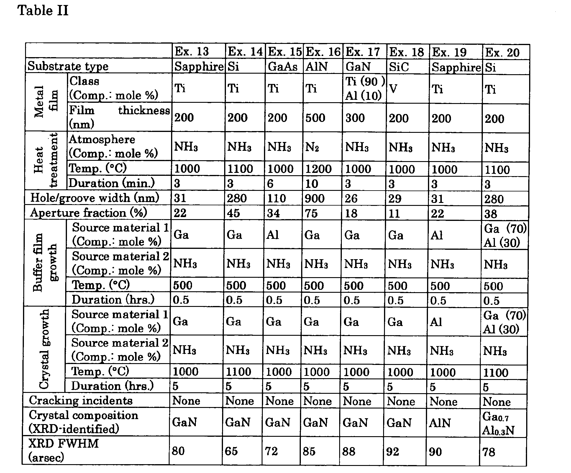
- a 200 nm-thick metallic Ti film was deposited as a metal film 2 on a substrate 1, as illustrated in Fig. 2A, using a sapphire base as the substrate 1.
- the metal film 2 was heat-treated in a NH 3 atmosphere at 1000°C for 3 minutes. the surface of the metal film 2 after its temperature was lowered was observed with an SEM. Holes or grooves in a worm-eaten pattern as shown in Fig. 3A were found; the average width W of the holes or grooves was 31 nm and the aperture fraction was 22%.
- a group III-V compound buffer film 3 as illustrated in Fig.
- the provision of a step of depositing a metal film on a substrate, a step of heat-treating the metal film in an atmosphere in which a patterning compound is present, and a step of growing a group III-V crystal on the metal film after the heat treatment yields good-quality group III-V crystals without causing cracks, using a simple and low-cost manufacturing method.
Landscapes
- Chemical & Material Sciences (AREA)
- Engineering & Computer Science (AREA)
- Crystallography & Structural Chemistry (AREA)
- Materials Engineering (AREA)
- Metallurgy (AREA)
- Organic Chemistry (AREA)
- Inorganic Chemistry (AREA)
- Chemical Kinetics & Catalysis (AREA)
- Physics & Mathematics (AREA)
- General Chemical & Material Sciences (AREA)
- Condensed Matter Physics & Semiconductors (AREA)
- General Physics & Mathematics (AREA)
- Electromagnetism (AREA)
- Optics & Photonics (AREA)
- Crystals, And After-Treatments Of Crystals (AREA)
- Chemical Vapour Deposition (AREA)
- Recrystallisation Techniques (AREA)
- Semiconductor Lasers (AREA)
- Led Devices (AREA)
Abstract
Description


Claims (9)
- A method of manufacturing a group III-V crystal, characterized in comprising: a step of depositing a metal film on a substrate; a step of heat-treating the metal film under an atmosphere in which a patterning compound is present; and a step of growing a group III-V crystal on the post-heat-treated metal film.
- A method of manufacturing a group III-V crystal, characterized in comprising: a step of depositing a metal film on a substrate; a step of heat-treating the metal film under an atmosphere in which a patterning compound is present; a step of growing a group III-V compound buffer film on the post-heat-treated metal film; and a step of growing a group III-V crystal on the group III-V compound buffer film.
- A group III-V crystal manufacturing method as set forth in either claim 1 or 2, characterized in that holes or grooves formed in the metal film by the heat-treating of the metal film under an atmosphere in which a patterning compound is present have an average width of 2 nm to 5000 nm, and the aperture fraction, being the percentage of the surface area that the holes or grooves occupy with respect to the substrate total surface area, is 5% to 80%.
- A group III-V crystal manufacturing method as set forth in any of claims 1 to 3, characterized in that the substrate is silicon, sapphire, SiC, ZrB2, or a group III-V compound.
- A group III-V crystal manufacturing method as set forth in any of claims 1 to 4, characterized in that the metal film contains titanium or vanadium.
- A group III-V crystal manufacturing method as set forth in any of claims 1 to 5, rendering the thickness of the metal film 10 nm to 1000 nm.
- A group III-V crystal manufacturing method as set forth in any of claims 1 to 6, characterized in that the heat treatment is carried out at 800°C to 1200°C for 0.5 minutes to 20 minutes.
- A group III-V compound crystal manufactured by a group III-V crystal manufacturing method as set forth in any of claims 1 to 7.
- A group III-V compound crystal as set forth in claim 8, the III-V crystal being GaxAlyIn1-x-y (0 ≤ x ≤ 1 and 0 ≤ y ≤ 1).
Applications Claiming Priority (3)
| Application Number | Priority Date | Filing Date | Title |
|---|---|---|---|
| JP2003129829 | 2003-05-08 | ||
| JP2003129829A JP4457576B2 (en) | 2003-05-08 | 2003-05-08 | Group III-V compound crystal and method for producing the same |
| PCT/JP2004/004811 WO2004099472A1 (en) | 2003-05-08 | 2004-04-01 | Iii-v compound semiconductor crystal and method for production thereof |
Publications (2)
| Publication Number | Publication Date |
|---|---|
| EP1522612A1 true EP1522612A1 (en) | 2005-04-13 |
| EP1522612A4 EP1522612A4 (en) | 2008-09-03 |
Family
ID=33432087
Family Applications (1)
| Application Number | Title | Priority Date | Filing Date |
|---|---|---|---|
| EP04725190A Withdrawn EP1522612A4 (en) | 2003-05-08 | 2004-04-01 | COMPOUND III-V SEMICONDUCTOR CRYSTAL AND PROCESS FOR PRODUCING THE SAME |
Country Status (6)
| Country | Link |
|---|---|
| US (3) | US7297625B2 (en) |
| EP (1) | EP1522612A4 (en) |
| JP (1) | JP4457576B2 (en) |
| CN (2) | CN101071794B (en) |
| TW (1) | TW200503076A (en) |
| WO (1) | WO2004099472A1 (en) |
Cited By (1)
| Publication number | Priority date | Publication date | Assignee | Title |
|---|---|---|---|---|
| EP3428957A1 (en) * | 2013-12-20 | 2019-01-16 | Huawei Technologies Co., Ltd. | Method for producing semiconductor device |
Families Citing this family (27)
| Publication number | Priority date | Publication date | Assignee | Title |
|---|---|---|---|---|
| JP4457576B2 (en) * | 2003-05-08 | 2010-04-28 | 住友電気工業株式会社 | Group III-V compound crystal and method for producing the same |
| JP4396816B2 (en) | 2003-10-17 | 2010-01-13 | 日立電線株式会社 | Group III nitride semiconductor substrate and manufacturing method thereof |
| JP2007027417A (en) * | 2005-07-15 | 2007-02-01 | Sanken Electric Co Ltd | Nitride semiconductor device and manufacturing method thereof |
| JP5057774B2 (en) * | 2006-12-26 | 2012-10-24 | 京セラ株式会社 | LIGHT EMITTING ELEMENT AND LIGHTING DEVICE |
| WO2009031276A1 (en) * | 2007-09-03 | 2009-03-12 | Sophia School Corporation | Iii nitride structure and method for manufacturing iii nitride semiconductor fine columnar crystal |
| US8927392B2 (en) | 2007-11-02 | 2015-01-06 | Siva Power, Inc. | Methods for forming crystalline thin-film photovoltaic structures |
| JP2010042981A (en) | 2008-07-17 | 2010-02-25 | Sumitomo Electric Ind Ltd | METHOD FOR PRODUCING AlGaN BULK CRYSTAL AND METHOD FOR PRODUCING AlGaN SUBSTRATE |
| US8803189B2 (en) * | 2008-08-11 | 2014-08-12 | Taiwan Semiconductor Manufacturing Company, Ltd. | III-V compound semiconductor epitaxy using lateral overgrowth |
| WO2010088366A1 (en) | 2009-01-28 | 2010-08-05 | Wakonda Technologies, Inc. | Large-grain crystalline thin-film structures and devices and methods for forming the same |
| US8507304B2 (en) | 2009-07-17 | 2013-08-13 | Applied Materials, Inc. | Method of forming a group III-nitride crystalline film on a patterned substrate by hydride vapor phase epitaxy (HVPE) |
| US20110027973A1 (en) * | 2009-07-31 | 2011-02-03 | Applied Materials, Inc. | Method of forming led structures |
| US8148241B2 (en) * | 2009-07-31 | 2012-04-03 | Applied Materials, Inc. | Indium surfactant assisted HVPE of high quality gallium nitride and gallium nitride alloy films |
| JP2012054364A (en) * | 2010-08-31 | 2012-03-15 | Nobuyuki Akiyama | Manufacturing method of silicon thin film, manufacturing method of silicon thin film solar cell, silicon thin film, silicon thin film solar cell |
| KR101207412B1 (en) * | 2011-06-20 | 2012-12-04 | 삼성코닝정밀소재 주식회사 | Gan substrate and method for maufacturing the same |
| JP6051524B2 (en) * | 2012-01-18 | 2016-12-27 | セイコーエプソン株式会社 | Semiconductor substrate and semiconductor substrate manufacturing method |
| JP2013203617A (en) * | 2012-03-29 | 2013-10-07 | Ngk Insulators Ltd | Method for manufacturing group 13 element nitride crystal, and laminate |
| KR101582021B1 (en) * | 2012-08-30 | 2015-12-31 | 엔지케이 인슐레이터 엘티디 | Composite substrates, a method of producing the same, a method of producing a functional layer of a nitride of a group 13 element and functional devices |
| JP2014067869A (en) * | 2012-09-26 | 2014-04-17 | Nobuyuki Akiyama | Manufacturing method of hetero-epitaxial single crystal, manufacturing method of heterojunction solar cell, hetero-epitaxial single crystal, and heterojunction solar cell |
| WO2016024514A1 (en) | 2014-08-12 | 2016-02-18 | Tdk株式会社 | Alumina substrate |
| JP6394170B2 (en) | 2014-08-12 | 2018-09-26 | Tdk株式会社 | Alumina substrate |
| CN104716241B (en) * | 2015-03-16 | 2018-10-16 | 映瑞光电科技(上海)有限公司 | A kind of LED structure and preparation method thereof |
| JP6503819B2 (en) | 2015-03-23 | 2019-04-24 | Tdk株式会社 | Alumina substrate |
| CN105826438B (en) * | 2016-06-01 | 2018-05-08 | 安徽三安光电有限公司 | A kind of light emitting diode with metal buffer layer and preparation method thereof |
| CN108736317B (en) * | 2018-05-15 | 2021-01-12 | 深圳市光脉电子有限公司 | Light emitting diode epitaxial structure and matrix type laser device thereof |
| US11056338B2 (en) | 2018-10-10 | 2021-07-06 | The Johns Hopkins University | Method for printing wide bandgap semiconductor materials |
| US11823900B2 (en) | 2018-10-10 | 2023-11-21 | The Johns Hopkins University | Method for printing wide bandgap semiconductor materials |
| CN110120448B (en) * | 2019-05-07 | 2021-05-25 | 厦门大学 | Nitride LED manufacturing method based on metal mask substrate |
Family Cites Families (20)
| Publication number | Priority date | Publication date | Assignee | Title |
|---|---|---|---|---|
| US5868837A (en) * | 1997-01-17 | 1999-02-09 | Cornell Research Foundation, Inc. | Low temperature method of preparing GaN single crystals |
| JP3934320B2 (en) * | 1997-03-13 | 2007-06-20 | 日本電気株式会社 | GaN-based semiconductor device and manufacturing method thereof |
| TW490441B (en) | 1998-06-12 | 2002-06-11 | Rohm & Haas | Lithium manganate composition |
| CN1077607C (en) * | 1998-11-03 | 2002-01-09 | 南京大学 | Method and installation for GaN growth by light radiation-heated metallic organic chemical gas-state deposition |
| JP3470623B2 (en) * | 1998-11-26 | 2003-11-25 | ソニー株式会社 | Method for growing nitride III-V compound semiconductor, method for manufacturing semiconductor device, and semiconductor device |
| JP3305310B1 (en) | 1998-12-09 | 2002-07-22 | 松下電器産業株式会社 | Temperature measurement method |
| JP3929657B2 (en) * | 1999-09-29 | 2007-06-13 | 株式会社リコー | Crystal growth method and group III nitride crystal production method |
| JP3519641B2 (en) | 1999-08-18 | 2004-04-19 | シャープ株式会社 | Semiconductor device having gold wiring and method of manufacturing the same |
| JP2001223165A (en) | 2000-02-10 | 2001-08-17 | Hitachi Cable Ltd | Nitride semiconductor and manufacturing method thereof |
| JP2002270516A (en) * | 2001-03-07 | 2002-09-20 | Nec Corp | Method of growing group III nitride semiconductor, group III nitride semiconductor film, and semiconductor device using the same |
| JP2002280314A (en) * | 2001-03-22 | 2002-09-27 | Toyoda Gosei Co Ltd | Method of manufacturing group III nitride compound semiconductor and group III nitride compound semiconductor device based thereon |
| JP2003007616A (en) * | 2001-03-23 | 2003-01-10 | Matsushita Electric Ind Co Ltd | Method for manufacturing semiconductor film |
| JP2002284600A (en) | 2001-03-26 | 2002-10-03 | Hitachi Cable Ltd | Gallium nitride crystal substrate manufacturing method and gallium nitride crystal substrate |
| JP3631724B2 (en) * | 2001-03-27 | 2005-03-23 | 日本電気株式会社 | Group III nitride semiconductor substrate and manufacturing method thereof |
| US6939730B2 (en) * | 2001-04-24 | 2005-09-06 | Sony Corporation | Nitride semiconductor, semiconductor device, and method of manufacturing the same |
| JP4575616B2 (en) | 2001-04-26 | 2010-11-04 | ルネサスエレクトロニクス株式会社 | Semiconductor device and manufacturing method thereof |
| JP3886341B2 (en) | 2001-05-21 | 2007-02-28 | 日本電気株式会社 | Method for manufacturing gallium nitride crystal substrate and gallium nitride crystal substrate |
| CN1167140C (en) * | 2002-05-17 | 2004-09-15 | 清华大学 | Substrate processing method for high-brightness GaN-based light-emitting diode epitaxial wafer |
| CN1174470C (en) * | 2002-05-31 | 2004-11-03 | 南京大学 | Method for growing high-quality GaN thin films by lateral epitaxial growth |
| JP4457576B2 (en) * | 2003-05-08 | 2010-04-28 | 住友電気工業株式会社 | Group III-V compound crystal and method for producing the same |
-
2003
- 2003-05-08 JP JP2003129829A patent/JP4457576B2/en not_active Expired - Fee Related
-
2004
- 2004-04-01 US US10/521,060 patent/US7297625B2/en not_active Expired - Fee Related
- 2004-04-01 WO PCT/JP2004/004811 patent/WO2004099472A1/en not_active Ceased
- 2004-04-01 CN CN200710102802.3A patent/CN101071794B/en not_active Expired - Fee Related
- 2004-04-01 CN CNB2004800006464A patent/CN1318661C/en not_active Expired - Fee Related
- 2004-04-01 EP EP04725190A patent/EP1522612A4/en not_active Withdrawn
- 2004-04-07 TW TW093109623A patent/TW200503076A/en not_active IP Right Cessation
-
2007
- 2007-10-12 US US11/871,162 patent/US7485484B2/en not_active Expired - Fee Related
-
2008
- 2008-08-08 US US12/188,214 patent/US20080299748A1/en not_active Abandoned
Cited By (2)
| Publication number | Priority date | Publication date | Assignee | Title |
|---|---|---|---|---|
| EP3428957A1 (en) * | 2013-12-20 | 2019-01-16 | Huawei Technologies Co., Ltd. | Method for producing semiconductor device |
| US10234629B2 (en) | 2013-12-20 | 2019-03-19 | Huawei Technologies Co., Ltd. | Method for reducing threading dislocation of semiconductor device |
Also Published As
| Publication number | Publication date |
|---|---|
| US20080038580A1 (en) | 2008-02-14 |
| EP1522612A4 (en) | 2008-09-03 |
| US20080299748A1 (en) | 2008-12-04 |
| CN1318661C (en) | 2007-05-30 |
| US7485484B2 (en) | 2009-02-03 |
| US7297625B2 (en) | 2007-11-20 |
| TW200503076A (en) | 2005-01-16 |
| TWI295481B (en) | 2008-04-01 |
| US20050227472A1 (en) | 2005-10-13 |
| JP4457576B2 (en) | 2010-04-28 |
| JP2004331453A (en) | 2004-11-25 |
| CN1697895A (en) | 2005-11-16 |
| CN101071794A (en) | 2007-11-14 |
| WO2004099472A1 (en) | 2004-11-18 |
| CN101071794B (en) | 2010-09-01 |
Similar Documents
| Publication | Publication Date | Title |
|---|---|---|
| US7485484B2 (en) | Group III-V crystal | |
| JP5135501B2 (en) | Manufacturing method of nitride single crystal substrate and manufacturing method of nitride semiconductor light emitting device using the same | |
| CN100530543C (en) | Epitaxial growth method | |
| KR100838433B1 (en) | Method for producing gallium nitride crystal substrate and gallium nitride crystal substrate | |
| JP4117156B2 (en) | Method for manufacturing group III nitride semiconductor substrate | |
| KR100682879B1 (en) | Crystal growth method | |
| KR101321654B1 (en) | Substrate for growing group-iii nitride semiconductors, epitaxial substrate for group-iii nitride semiconductors, group-iii nitride semiconductor element, stand-alone substrate for group-iii nitride semiconductors, and methods for manufacturing the preceding | |
| US20050247260A1 (en) | Non-polar single crystalline a-plane nitride semiconductor wafer and preparation thereof | |
| JP2002343728A (en) | Gallium nitride crystal substrate manufacturing method and gallium nitride crystal substrate | |
| JP2002505519A (en) | Method for producing gallium nitride semiconductor layer by lateral overgrowth through mask and gallium nitride semiconductor structure produced thereby | |
| KR101503618B1 (en) | Method for producing substrate for group iii nitride semiconductor element fabrication, method for producing group iii nitride semiconductor free-standing substrate or group iii nitride semiconductor element, and group iii nitride growth substrate | |
| CN102245814A (en) | Manufacturing method of nitride-based compound semiconductor substrate and nitride-based compound semiconductor self-supporting substrate | |
| JP4301592B2 (en) | Manufacturing method of substrate with nitride semiconductor layer | |
| JP2010280562A (en) | Group III nitride crystal manufacturing method, group III nitride crystal substrate, and group III nitride semiconductor device | |
| JP2002050585A (en) | Semiconductor crystal growth method | |
| KR101358541B1 (en) | Ⅲ-nitride semiconductor growth substrate, ⅲ-nitride semiconductor epitaxial substrate, ⅲ-nitride semiconductor element, ⅲ-nitride semiconductor freestanding substrate, and method for fabricating these | |
| US8134223B2 (en) | III-V compound crystal and semiconductor electronic circuit element | |
| JP2023532799A (en) | Semiconductor substrate with nitrided interfacial layer | |
| TW200907124A (en) | Method for forming group-III nitride semiconductor epilayer on silicon substrate | |
| JP2003171200A (en) | Compound semiconductor crystal growth method and compound semiconductor device | |
| JP2009292718A (en) | Group iii-v compound crystal-containing material and method for producing group iii-v compound crystal | |
| JP2002231640A (en) | Gallium nitride substrate and method of manufacturing the same |
Legal Events
| Date | Code | Title | Description |
|---|---|---|---|
| PUAI | Public reference made under article 153(3) epc to a published international application that has entered the european phase |
Free format text: ORIGINAL CODE: 0009012 |
|
| 17P | Request for examination filed |
Effective date: 20050127 |
|
| AK | Designated contracting states |
Kind code of ref document: A1 Designated state(s): AT BE BG CH CY CZ DE DK EE ES FI FR GB GR HU IE IT LI LU MC NL PL PT RO SE SI SK TR |
|
| AX | Request for extension of the european patent |
Extension state: AL HR LT LV MK |
|
| DAX | Request for extension of the european patent (deleted) | ||
| RBV | Designated contracting states (corrected) |
Designated state(s): DE FR GB |
|
| A4 | Supplementary search report drawn up and despatched |
Effective date: 20080801 |
|
| 17Q | First examination report despatched |
Effective date: 20081219 |
|
| STAA | Information on the status of an ep patent application or granted ep patent |
Free format text: STATUS: THE APPLICATION IS DEEMED TO BE WITHDRAWN |
|
| 18D | Application deemed to be withdrawn |
Effective date: 20110225 |