EP1521986B1 - Thermal compensation of waveguides by dual material core - Google Patents
Thermal compensation of waveguides by dual material core Download PDFInfo
- Publication number
- EP1521986B1 EP1521986B1 EP03731473A EP03731473A EP1521986B1 EP 1521986 B1 EP1521986 B1 EP 1521986B1 EP 03731473 A EP03731473 A EP 03731473A EP 03731473 A EP03731473 A EP 03731473A EP 1521986 B1 EP1521986 B1 EP 1521986B1
- Authority
- EP
- European Patent Office
- Prior art keywords
- core
- region
- lightwave circuit
- planar lightwave
- polymer
- Prior art date
- Legal status (The legal status is an assumption and is not a legal conclusion. Google has not performed a legal analysis and makes no representation as to the accuracy of the status listed.)
- Expired - Lifetime
Links
Images


Classifications
-
- G—PHYSICS
- G02—OPTICS
- G02B—OPTICAL ELEMENTS, SYSTEMS OR APPARATUS
- G02B6/00—Light guides; Structural details of arrangements comprising light guides and other optical elements, e.g. couplings
- G02B6/10—Light guides; Structural details of arrangements comprising light guides and other optical elements, e.g. couplings of the optical waveguide type
- G02B6/12—Light guides; Structural details of arrangements comprising light guides and other optical elements, e.g. couplings of the optical waveguide type of the integrated circuit kind
- G02B6/122—Basic optical elements, e.g. light-guiding paths
- G02B6/1221—Basic optical elements, e.g. light-guiding paths made from organic materials
-
- G—PHYSICS
- G02—OPTICS
- G02B—OPTICAL ELEMENTS, SYSTEMS OR APPARATUS
- G02B6/00—Light guides; Structural details of arrangements comprising light guides and other optical elements, e.g. couplings
- G02B6/10—Light guides; Structural details of arrangements comprising light guides and other optical elements, e.g. couplings of the optical waveguide type
- G02B6/12—Light guides; Structural details of arrangements comprising light guides and other optical elements, e.g. couplings of the optical waveguide type of the integrated circuit kind
- G02B6/12007—Light guides; Structural details of arrangements comprising light guides and other optical elements, e.g. couplings of the optical waveguide type of the integrated circuit kind forming wavelength selective elements, e.g. multiplexer, demultiplexer
-
- G—PHYSICS
- G02—OPTICS
- G02B—OPTICAL ELEMENTS, SYSTEMS OR APPARATUS
- G02B6/00—Light guides; Structural details of arrangements comprising light guides and other optical elements, e.g. couplings
- G02B6/10—Light guides; Structural details of arrangements comprising light guides and other optical elements, e.g. couplings of the optical waveguide type
- G02B6/12—Light guides; Structural details of arrangements comprising light guides and other optical elements, e.g. couplings of the optical waveguide type of the integrated circuit kind
- G02B6/122—Basic optical elements, e.g. light-guiding paths
Definitions
- the described invention relates to the field of optical circuits.
- the invention relates to thermal compensation in an optical waveguide.
- Optical circuits include, but are not limited to, light sources, detectors and/or waveguides that provide such functions as splitting, coupling, combining, multiplexing, demultiplexing, and switching.
- Planar lightwave circuits(PLCs) are optical circuits that are manufactured and operate in the plane of a wafer. PLC technology is advantageous because it can be used to form many different types of optical devices, such as array waveguide grating (AWG) filters, optical add/drop (de) multiplexers, optical switches, monolithic, as well as hybrid opto-electronic integrated devices. Such devices formed with optical fibers would typically be much larger or would not be feasible at all. Further, PLC structures may be mass produced on a silicon wafer.
- PLCs often have been based on silica-on-silicon (SOS) technology, but may alternatively be implemented using other technologies such as, but not limited to, siliconon-insulator (SOI), polymer on silicon, and so forth.
- SOS silica-on-silicon
- SOI siliconon-insulator
- Thermal compensation for some optical circuits is important as devices may be operated in locations where temperatures cannot be assured.
- optical circuits are combined with temperature regulating equipment.
- these configurations may be less than ideal, since the devices are prone to failure if there is a power outage, and temperature regulating equipment may require a large amount of power which may not be desirable.
- US-B1-6311004 describes a photonic device pertaining to the features of the preamble of claim 1.
- a planar lightwave circuit comprises one or more waveguides that are thermally-compensating.
- the thermally-compensating waveguides comprise a cladding and a core that comprises two regions running lengthwise through the core. One region has a negative thermo-optic coefficient ("TOC"); the other region has a positive TOC.
- TOC thermo-optic coefficient
- Figure 1A is a schematic diagram showing one embodiment of a cross-sectional view of a waveguide structure 5.
- the structure is subsequently modified as described with respect to Figures 1B and 1C to be thermally-compensating.
- a layer of lower cladding 12 is typically deposited onto a substrate 10.
- a waveguide core layer 20 is deposited over the lower cladding 12, and an upper cladding 24 is deposited over the waveguide core layer 20.
- the substrate 10 is silicon
- the lower cladding 12 is SiO 2
- the core layer 20 is SiO 2 doped with Germanium
- the upper cladding 24 is a borophosphosilicate glass (BPSG).
- the upper cladding 24 may form a thin layer of approximately 1-2 microns covering the core.
- Figure 1B is a schematic diagram showing one embodiment of a cross-section view of a waveguide after a trench 30 is created in the core layer 20.
- the trench 30 is formed to run along a length of the core of the waveguide.
- the trench may be formed by etching, ion beam milling, or other methods.
- the trench has a depth of at least 2/3 of the depth of the core. However, the trench depth may extend down into the lower cladding 12.
- the width of the trench is designed to be less than a wavelength of the optical signal to be propagated by the waveguide.
- Figure 1C is a schematic diagram showing one embodiment of a cross-sectional view of Figure 1B after a layer of material 50 having a negative TOC has been deposited.
- the negative TOC material 50 fills the trench to form a negative TOC center region 40 of the core.
- a polymer such as silicone, poly(methylmethacrylate) (“PMMA”), or benzocyclobutene (“BCB”).
- PMMA poly(methylmethacrylate)
- BCB benzocyclobutene
- various other materials may alternatively be used.
- a first portion of the optical field of the optical signal propagates in the negative TOC region 40, and a second portion of the optical field propagates in the positive TOC region 42 of the core.
- the first portion of the optical field in the negative TOC region 40 is substantially surrounded by the second portion of the optical field in the positive TOC region 42.
- the refractive index difference between the negative TOC region 40 and the positive TOC region 42 is large enough to allow filling over the negative TOC region 40 with a layer of the same material that serves as an upper cladding.
- the structure described provides good compensation with low loss over a wide temperature range, and allows for convenient fabrication.
- FIG. 2 is a flowchart showing one embodiment of a method for fabricating a thermally-compensating waveguide.
- the flowchart starts at block 100, and continues with block 110, at which a core of the waveguide is formed over an appropriate substrate structure.
- the core is formed on a SOS structure and comprises SiO 2 doped with Germanium having a cross-sectional area of approximately 6 microns by 6 microns. Other positive TOC materials may alternatively be used.
- the flowchart continues at block 120 at which a trench is created in the core. In one embodiment, the trench is approximately 1 micron wide and runs an entire length of the waveguide.
- a negative thermo-optic coefficient material is deposited into the trench. In one embodiment, an optical signal of approximately 1550 nm propagates within both the materials making up the core, having both positive and negative TOC regions.
- the flowchart ends at block 140.
- another material having a positive TOC may be used to cover the negative TOC material.
- the effective index of propagation in the core will have a close to linear response to compensate for the thermal expansion of the substrate, and allows for thermal compensation up to a range of approximately 100 °C. Additionally, the described waveguide structure may be used for curved waveguides. A bend radius of down to 10 mm is achievable with losses on the order of approximately .3 db/cm.
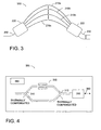
- FIG. 3 is a schematic diagram showing one embodiment of an array waveguide grating (AWG) 200 that makes use of thermally-compensating waveguides.
- the waveguides 210a-210x are thenmally-compensating as previously described, but the star couplers 220 and 222 and the input and output waveguides 230 and 232 are not thermally-compensated, allowing for easier alignment of the input and output waveguides 230 and 232 with other optical components.
- Figure 4 is a schematic diagram showing an embodiment of a PLC comprising an interferometric component 300 that uses thermally-compensating waveguides in coupler regions 310 and 312.
- a temperature regulator 320 is used on a non-thermally-compensated waveguide portion to modify the phase of the optical signal.
- an electrical component 350 such as an optical-to-electrical converter and/or electrical-to-optical converter, is coupled to the thermally-compensated waveguide coupler 312.
- One or more electrical connections 360 couple the electrical component 350 with power and other electrical signals.
- the phase modulation may be adjusted using other methods, such as mechanical.
- a temperature regulator 380 may be housed with a thermally-compensated optical circuit to keep the device within its thermally-compensating temperature range.
- thermally-compensating waveguides described compensate single mode waveguides independently. They may be used solely in a phase-sensitive portion or throughout an optical circuit.
- silicone has a TOC of -39x10-5/°C
- PMMA has a TOC of -9x10⁻⁵/°C
- BPSG has a TOC of approximately 1.2x10⁻⁵/°C.
- the design of the trench may be altered to compensate for the use of various materials.
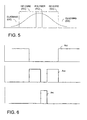
- Figure 5 is a graph illustrating the normalized mode field intensity in a cross section of a dual material waveguide.
- Figure 6 is a graph illustrating an aperture function for a dual material waveguide.
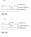
- Figures 7A-7C are schematic diagrams that illustrate another embodiment of a thermally compensated waveguide 505.
- the core 520 has a central portion that has a positive TOC and an outer portion that has a negative TOC.
- Figure 7A shows a first core portion 520a having a positive TOC.
- the first core portion 520a forms a spike running the length of a waveguide.
- the first core portion is formed on a lower cladding 512 over a substrate 510, similar to that of Figure 1A.
- the first core portion may be deposited and then etched to form a spike having the desired dimensions.
- Support structures 524 may be formed on the lower cladding 512 as long as they are far enough away from the core 520 to prevent light from leaking from the core to the support structure.
- Figure 7B shows a negative TOC material deposited over the positive TOC first core portion 520a to form a second core portion 520b.
- the first core portion 520a and the second core portion 520b make up the core 520.
- the negative TOC core material is a polymer ("core polymer").
- the core polymer is formed by spinning accumulation. Alternatively, the core polymer may be applied by other lithography methods.
- the core polymer has a refractive index of approximately 1.45 to 1.6.
- Figure 7C shows a second negative TOC material deposited over the core 520 to form a cladding 530.
- the negative TOC material is a polymer ("cladding polymer”) and has a refractive index approximately .01 to .05 less than that of the core polymer 520b.
- the core polymer and the cladding polymer are related polymers.
- Figure 7D is a schematic diagram showing an enlargement of the core 520 of the waveguide 505 of Figures 7A-7C.
- an undercladding 550 is deposited before applying the core polymer 520a. This provides an undercladding of polymer under the core, which creates an interface under the core that substantially matches the core/cladding interface on top of the core to provide better performance.
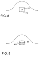
- Figure 8 is a schematic diagram showing a cross sectional view of another embodiment of a waveguide having a dual material core.
- an inner core 610 is completely surrounded by an outer core 612.
- the inner core has a positive TOC and the outer core has a negative TOC.
- the inner and outer cores may comprise polymer or other suitable materials.
- Figure 9 is a schematic diagram showing a cross section view of another embodiment of a waveguide having a dual material core.
- an inner core 620 is sandwiched between an outer core 622.
- the inner core lies substantially in the plane of the substrate of the PLC, and will not have as good optical confinement for PLC's with significant bend radii compared to the structures previously described with respect to Figures 1C and 7C having inner cores in a plane substantially perpendicular to the plane of the substrate of the PLC.
Landscapes
- Physics & Mathematics (AREA)
- Engineering & Computer Science (AREA)
- Microelectronics & Electronic Packaging (AREA)
- General Physics & Mathematics (AREA)
- Optics & Photonics (AREA)
- Optical Integrated Circuits (AREA)
- Non-Reversible Transmitting Devices (AREA)
Applications Claiming Priority (3)
| Application Number | Priority Date | Filing Date | Title |
|---|---|---|---|
| US10/190,411 US6987895B2 (en) | 2002-07-02 | 2002-07-02 | Thermal compensation of waveguides by dual material core having positive thermo-optic coefficient inner core |
| US190411 | 2002-07-02 | ||
| PCT/US2003/017180 WO2004005988A1 (en) | 2002-07-02 | 2003-05-29 | Thermal compensation of waveguides by dual material core |
Publications (2)
| Publication Number | Publication Date |
|---|---|
| EP1521986A1 EP1521986A1 (en) | 2005-04-13 |
| EP1521986B1 true EP1521986B1 (en) | 2007-05-09 |
Family
ID=29999877
Family Applications (1)
| Application Number | Title | Priority Date | Filing Date |
|---|---|---|---|
| EP03731473A Expired - Lifetime EP1521986B1 (en) | 2002-07-02 | 2003-05-29 | Thermal compensation of waveguides by dual material core |
Country Status (7)
| Country | Link |
|---|---|
| US (1) | US6987895B2 (https=) |
| EP (1) | EP1521986B1 (https=) |
| JP (1) | JP4221364B2 (https=) |
| AT (1) | ATE362123T1 (https=) |
| AU (1) | AU2003240968A1 (https=) |
| DE (1) | DE60313776T2 (https=) |
| WO (1) | WO2004005988A1 (https=) |
Families Citing this family (21)
| Publication number | Priority date | Publication date | Assignee | Title |
|---|---|---|---|---|
| US7006719B2 (en) * | 2002-03-08 | 2006-02-28 | Infinera Corporation | In-wafer testing of integrated optical components in photonic integrated circuits (PICs) |
| US7194176B2 (en) * | 2002-05-29 | 2007-03-20 | Hoya Corporation | Functional optical devices and methods for producing them |
| US6987895B2 (en) | 2002-07-02 | 2006-01-17 | Intel Corporation | Thermal compensation of waveguides by dual material core having positive thermo-optic coefficient inner core |
| US20060140569A1 (en) * | 2004-12-28 | 2006-06-29 | Intel Corporation | Planar waveguides with air thin films used as anti-reflective layers, beam splitters and mirrors |
| US8496647B2 (en) | 2007-12-18 | 2013-07-30 | Intuitive Surgical Operations, Inc. | Ribbed force sensor |
| US20070003198A1 (en) * | 2005-06-29 | 2007-01-04 | Lance Gibson | Low loss optical fiber designs and methods for their manufacture |
| JP2007193049A (ja) * | 2006-01-18 | 2007-08-02 | Sony Corp | 光導波路及び光モジュール |
| US7406222B2 (en) * | 2006-02-16 | 2008-07-29 | Pavel Kornilovich | Composite evanescent waveguides and associated methods |
| US8285150B2 (en) | 2006-10-02 | 2012-10-09 | Futurewei Technologies, Inc. | Method and system for integrated DWDM transmitters |
| US8285149B2 (en) * | 2006-10-02 | 2012-10-09 | Futurewei Technologies, Inc. | Method and system for integrated DWDM transmitters |
| US8285151B2 (en) * | 2006-10-20 | 2012-10-09 | Futurewei Technologies, Inc. | Method and system for hybrid integrated 1XN DWDM transmitter |
| US8561473B2 (en) * | 2007-12-18 | 2013-10-22 | Intuitive Surgical Operations, Inc. | Force sensor temperature compensation |
| US8290325B2 (en) * | 2008-06-30 | 2012-10-16 | Intel Corporation | Waveguide photodetector device and manufacturing method thereof |
| KR20140096918A (ko) * | 2013-01-29 | 2014-08-06 | 삼성전자주식회사 | 온도 무의존성 도파로 및 그 제조 방법 |
| US10295739B2 (en) * | 2013-04-22 | 2019-05-21 | Cornell University | Athermal optical devices based on composite structures |
| CN110927992B (zh) * | 2019-12-20 | 2023-02-28 | 武汉邮电科学研究院有限公司 | 一种光开关 |
| CN110989078A (zh) * | 2019-12-25 | 2020-04-10 | 易锐光电科技(安徽)有限公司 | 薄膜光波导及其制备方法 |
| US11372157B2 (en) | 2020-09-30 | 2022-06-28 | Nokia Solutions And Networks Oy | Integrated optical multiplexer / demultiplexer with thermal compensation |
| US11480729B2 (en) | 2020-10-30 | 2022-10-25 | Nokia Solutions And Networks Oy | Thermally compensated slot waveguide |
| US20220276437A1 (en) * | 2022-05-18 | 2022-09-01 | Intel Corporation | Temperature insensitive waveguides and array waveguide grating mux/demux devices |
| US12596288B2 (en) * | 2023-08-31 | 2026-04-07 | Nexus Photonics, Inc | Temperature stabilized dielectric based on-chip interferometers |
Family Cites Families (18)
| Publication number | Priority date | Publication date | Assignee | Title |
|---|---|---|---|---|
| US5163118A (en) * | 1986-11-10 | 1992-11-10 | The United States Of America As Represented By The Secretary Of The Air Force | Lattice mismatched hetrostructure optical waveguide |
| US5125946A (en) * | 1990-12-10 | 1992-06-30 | Corning Incorporated | Manufacturing method for planar optical waveguides |
| FR2746511B1 (fr) * | 1996-03-20 | 1998-04-24 | Bosc Dominique | Coupleur directif actif mixte silice/polymere, en optique integree |
| US6144779A (en) * | 1997-03-11 | 2000-11-07 | Lightwave Microsystems Corporation | Optical interconnects with hybrid construction |
| US6122416A (en) * | 1997-09-26 | 2000-09-19 | Nippon Telegraph And Telephone Corporation | Stacked thermo-optic switch, switch matrix and add-drop multiplexer having the stacked thermo-optic switch |
| US6137939A (en) * | 1997-10-01 | 2000-10-24 | Lucent Technologies Inc. | Method and apparatus for reducing temperature-related spectrum shifts in optical devices |
| US6083843A (en) * | 1997-12-16 | 2000-07-04 | Northern Telecom Limited | Method of manufacturing planar lightwave circuits |
| US6002823A (en) * | 1998-08-05 | 1999-12-14 | Lucent Techolonogies Inc. | Tunable directional optical waveguide couplers |
| US6240226B1 (en) * | 1998-08-13 | 2001-05-29 | Lucent Technologies Inc. | Polymer material and method for optical switching and modulation |
| US6310999B1 (en) * | 1998-10-05 | 2001-10-30 | Lucent Technologies Inc. | Directional coupler and method using polymer material |
| US6311004B1 (en) * | 1998-11-10 | 2001-10-30 | Lightwave Microsystems | Photonic devices comprising thermo-optic polymer |
| EP1026526A1 (en) | 1999-02-02 | 2000-08-09 | Corning Incorporated | Athermalized polymer overclad integrated planar optical waveguide device and its manufacturing method |
| CA2271159A1 (en) * | 1999-04-30 | 2000-10-30 | Jds Fitel Inc. | Optical hybrid device |
| CA2314420C (en) * | 1999-07-27 | 2008-06-03 | Sumitomo Electric Industries, Ltd. | Optical filter |
| US6389209B1 (en) * | 1999-09-07 | 2002-05-14 | Agere Systems Optoelectronics Guardian Corp. | Strain free planar optical waveguides |
| US6704487B2 (en) * | 2001-08-10 | 2004-03-09 | Lightwave Microsystems Corporation | Method and system for reducing dn/dt birefringence in a thermo-optic PLC device |
| US20040005108A1 (en) | 2002-07-02 | 2004-01-08 | Kjetil Johannessen | Thermal compensation of waveguides by dual material core having negative thermo-optic coefficient inner core |
| US6987895B2 (en) | 2002-07-02 | 2006-01-17 | Intel Corporation | Thermal compensation of waveguides by dual material core having positive thermo-optic coefficient inner core |
-
2002
- 2002-07-02 US US10/190,411 patent/US6987895B2/en not_active Expired - Fee Related
-
2003
- 2003-05-29 DE DE60313776T patent/DE60313776T2/de not_active Expired - Lifetime
- 2003-05-29 AT AT03731473T patent/ATE362123T1/de not_active IP Right Cessation
- 2003-05-29 JP JP2004519571A patent/JP4221364B2/ja not_active Expired - Fee Related
- 2003-05-29 EP EP03731473A patent/EP1521986B1/en not_active Expired - Lifetime
- 2003-05-29 WO PCT/US2003/017180 patent/WO2004005988A1/en not_active Ceased
- 2003-05-29 AU AU2003240968A patent/AU2003240968A1/en not_active Abandoned
Non-Patent Citations (1)
| Title |
|---|
| None * |
Also Published As
| Publication number | Publication date |
|---|---|
| US6987895B2 (en) | 2006-01-17 |
| ATE362123T1 (de) | 2007-06-15 |
| WO2004005988A1 (en) | 2004-01-15 |
| JP2005531818A (ja) | 2005-10-20 |
| DE60313776T2 (de) | 2008-01-24 |
| JP4221364B2 (ja) | 2009-02-12 |
| US20040005133A1 (en) | 2004-01-08 |
| AU2003240968A1 (en) | 2004-01-23 |
| DE60313776D1 (de) | 2007-06-21 |
| EP1521986A1 (en) | 2005-04-13 |
Similar Documents
| Publication | Publication Date | Title |
|---|---|---|
| EP1521986B1 (en) | Thermal compensation of waveguides by dual material core | |
| US6704487B2 (en) | Method and system for reducing dn/dt birefringence in a thermo-optic PLC device | |
| Lee et al. | Temperature dependence of silicon nanophotonic ring resonator with a polymeric overlayer | |
| Li et al. | Silica-based optical integrated circuits | |
| US8532441B2 (en) | Optical device for wavelength locking | |
| US7006744B2 (en) | Hybrid buried/ridge planar waveguides | |
| US7221825B2 (en) | Optical coupler | |
| Pearson et al. | Arrayed waveguide grating demultiplexers in silicon-on-insulator | |
| Jalali et al. | Guided-wave optics in silicon-on-insulator technology | |
| US20020159702A1 (en) | Optical mach-zehnder interferometers with low polarization dependence | |
| Cheben et al. | Polarization compensation in silicon-on-insulator arrayed waveguide grating devices | |
| US20040005108A1 (en) | Thermal compensation of waveguides by dual material core having negative thermo-optic coefficient inner core | |
| Aalto et al. | Fast thermo-optical switch based on SOI waveguides | |
| Bozeat et al. | Silicon based waveguides | |
| US20210405292A1 (en) | Optical Interconnect Structure and Method for Manufacturing Same | |
| US11372157B2 (en) | Integrated optical multiplexer / demultiplexer with thermal compensation | |
| US20040151459A1 (en) | Method of polarisation compensation in grating- and phasar-based devices by using over-layer deposited on the compensating region to modify local slab waveguide birefringence | |
| Mottier | Integrated optics and micro-optics at LETI | |
| Jalali | Silicon-on-insulator photonic integrated circuit (SOI-PIC) technology | |
| Eldada | Photonic integrated circuits | |
| US6928215B1 (en) | Optical tap for optical integrated circuits | |
| Trinh et al. | Guided-wave optical circuits in silicon-on-insulator technology | |
| Winnie et al. | Polymer-cladded athermal high-index-contrast waveguides | |
| Xu et al. | Polarization-insensitive MMI-coupled ring resonators in silicon-on-insulator using cladding stress engineering | |
| Kauffman et al. | Length minimization in integrated optical circuits incorporating directional couplers and curved sections |
Legal Events
| Date | Code | Title | Description |
|---|---|---|---|
| PUAI | Public reference made under article 153(3) epc to a published international application that has entered the european phase |
Free format text: ORIGINAL CODE: 0009012 |
|
| 17P | Request for examination filed |
Effective date: 20050131 |
|
| AK | Designated contracting states |
Kind code of ref document: A1 Designated state(s): AT BE BG CH CY CZ DE DK EE ES FI FR GB GR HU IE IT LI LU MC NL PT RO SE SI SK TR |
|
| AX | Request for extension of the european patent |
Extension state: AL LT LV MK |
|
| 17Q | First examination report despatched |
Effective date: 20050408 |
|
| DAX | Request for extension of the european patent (deleted) | ||
| GRAP | Despatch of communication of intention to grant a patent |
Free format text: ORIGINAL CODE: EPIDOSNIGR1 |
|
| GRAS | Grant fee paid |
Free format text: ORIGINAL CODE: EPIDOSNIGR3 |
|
| GRAA | (expected) grant |
Free format text: ORIGINAL CODE: 0009210 |
|
| AK | Designated contracting states |
Kind code of ref document: B1 Designated state(s): AT BE BG CH CY CZ DE DK EE ES FI FR GB GR HU IE IT LI LU MC NL PT RO SE SI SK TR |
|
| PG25 | Lapsed in a contracting state [announced via postgrant information from national office to epo] |
Ref country code: CH Free format text: LAPSE BECAUSE OF FAILURE TO SUBMIT A TRANSLATION OF THE DESCRIPTION OR TO PAY THE FEE WITHIN THE PRESCRIBED TIME-LIMIT Effective date: 20070509 Ref country code: LI Free format text: LAPSE BECAUSE OF FAILURE TO SUBMIT A TRANSLATION OF THE DESCRIPTION OR TO PAY THE FEE WITHIN THE PRESCRIBED TIME-LIMIT Effective date: 20070509 Ref country code: FI Free format text: LAPSE BECAUSE OF FAILURE TO SUBMIT A TRANSLATION OF THE DESCRIPTION OR TO PAY THE FEE WITHIN THE PRESCRIBED TIME-LIMIT Effective date: 20070509 |
|
| REG | Reference to a national code |
Ref country code: GB Ref legal event code: FG4D |
|
| REG | Reference to a national code |
Ref country code: CH Ref legal event code: EP |
|
| REG | Reference to a national code |
Ref country code: IE Ref legal event code: FG4D |
|
| REF | Corresponds to: |
Ref document number: 60313776 Country of ref document: DE Date of ref document: 20070621 Kind code of ref document: P |
|
| PG25 | Lapsed in a contracting state [announced via postgrant information from national office to epo] |
Ref country code: SE Free format text: LAPSE BECAUSE OF FAILURE TO SUBMIT A TRANSLATION OF THE DESCRIPTION OR TO PAY THE FEE WITHIN THE PRESCRIBED TIME-LIMIT Effective date: 20070809 |
|
| PG25 | Lapsed in a contracting state [announced via postgrant information from national office to epo] |
Ref country code: ES Free format text: LAPSE BECAUSE OF FAILURE TO SUBMIT A TRANSLATION OF THE DESCRIPTION OR TO PAY THE FEE WITHIN THE PRESCRIBED TIME-LIMIT Effective date: 20070820 |
|
| NLV1 | Nl: lapsed or annulled due to failure to fulfill the requirements of art. 29p and 29m of the patents act | ||
| REG | Reference to a national code |
Ref country code: CH Ref legal event code: PL |
|
| PG25 | Lapsed in a contracting state [announced via postgrant information from national office to epo] |
Ref country code: AT Free format text: LAPSE BECAUSE OF FAILURE TO SUBMIT A TRANSLATION OF THE DESCRIPTION OR TO PAY THE FEE WITHIN THE PRESCRIBED TIME-LIMIT Effective date: 20070509 |
|
| PG25 | Lapsed in a contracting state [announced via postgrant information from national office to epo] |
Ref country code: BE Free format text: LAPSE BECAUSE OF FAILURE TO SUBMIT A TRANSLATION OF THE DESCRIPTION OR TO PAY THE FEE WITHIN THE PRESCRIBED TIME-LIMIT Effective date: 20070509 |
|
| EN | Fr: translation not filed | ||
| PG25 | Lapsed in a contracting state [announced via postgrant information from national office to epo] |
Ref country code: CZ Free format text: LAPSE BECAUSE OF FAILURE TO SUBMIT A TRANSLATION OF THE DESCRIPTION OR TO PAY THE FEE WITHIN THE PRESCRIBED TIME-LIMIT Effective date: 20070509 Ref country code: PT Free format text: LAPSE BECAUSE OF FAILURE TO SUBMIT A TRANSLATION OF THE DESCRIPTION OR TO PAY THE FEE WITHIN THE PRESCRIBED TIME-LIMIT Effective date: 20071009 Ref country code: NL Free format text: LAPSE BECAUSE OF FAILURE TO SUBMIT A TRANSLATION OF THE DESCRIPTION OR TO PAY THE FEE WITHIN THE PRESCRIBED TIME-LIMIT Effective date: 20070509 Ref country code: MC Free format text: LAPSE BECAUSE OF NON-PAYMENT OF DUE FEES Effective date: 20070531 Ref country code: BG Free format text: LAPSE BECAUSE OF FAILURE TO SUBMIT A TRANSLATION OF THE DESCRIPTION OR TO PAY THE FEE WITHIN THE PRESCRIBED TIME-LIMIT Effective date: 20070809 Ref country code: DK Free format text: LAPSE BECAUSE OF FAILURE TO SUBMIT A TRANSLATION OF THE DESCRIPTION OR TO PAY THE FEE WITHIN THE PRESCRIBED TIME-LIMIT Effective date: 20070509 Ref country code: SI Free format text: LAPSE BECAUSE OF FAILURE TO SUBMIT A TRANSLATION OF THE DESCRIPTION OR TO PAY THE FEE WITHIN THE PRESCRIBED TIME-LIMIT Effective date: 20070509 |
|
| PG25 | Lapsed in a contracting state [announced via postgrant information from national office to epo] |
Ref country code: SK Free format text: LAPSE BECAUSE OF FAILURE TO SUBMIT A TRANSLATION OF THE DESCRIPTION OR TO PAY THE FEE WITHIN THE PRESCRIBED TIME-LIMIT Effective date: 20070509 |
|
| PLBE | No opposition filed within time limit |
Free format text: ORIGINAL CODE: 0009261 |
|
| STAA | Information on the status of an ep patent application or granted ep patent |
Free format text: STATUS: NO OPPOSITION FILED WITHIN TIME LIMIT |
|
| 26N | No opposition filed |
Effective date: 20080212 |
|
| PG25 | Lapsed in a contracting state [announced via postgrant information from national office to epo] |
Ref country code: GR Free format text: LAPSE BECAUSE OF FAILURE TO SUBMIT A TRANSLATION OF THE DESCRIPTION OR TO PAY THE FEE WITHIN THE PRESCRIBED TIME-LIMIT Effective date: 20070810 Ref country code: IT Free format text: LAPSE BECAUSE OF FAILURE TO SUBMIT A TRANSLATION OF THE DESCRIPTION OR TO PAY THE FEE WITHIN THE PRESCRIBED TIME-LIMIT Effective date: 20070509 |
|
| PG25 | Lapsed in a contracting state [announced via postgrant information from national office to epo] |
Ref country code: IE Free format text: LAPSE BECAUSE OF NON-PAYMENT OF DUE FEES Effective date: 20070529 Ref country code: RO Free format text: LAPSE BECAUSE OF FAILURE TO SUBMIT A TRANSLATION OF THE DESCRIPTION OR TO PAY THE FEE WITHIN THE PRESCRIBED TIME-LIMIT Effective date: 20070509 |
|
| PG25 | Lapsed in a contracting state [announced via postgrant information from national office to epo] |
Ref country code: FR Free format text: LAPSE BECAUSE OF FAILURE TO SUBMIT A TRANSLATION OF THE DESCRIPTION OR TO PAY THE FEE WITHIN THE PRESCRIBED TIME-LIMIT Effective date: 20080104 |
|
| PG25 | Lapsed in a contracting state [announced via postgrant information from national office to epo] |
Ref country code: EE Free format text: LAPSE BECAUSE OF FAILURE TO SUBMIT A TRANSLATION OF THE DESCRIPTION OR TO PAY THE FEE WITHIN THE PRESCRIBED TIME-LIMIT Effective date: 20070509 |
|
| PG25 | Lapsed in a contracting state [announced via postgrant information from national office to epo] |
Ref country code: CY Free format text: LAPSE BECAUSE OF FAILURE TO SUBMIT A TRANSLATION OF THE DESCRIPTION OR TO PAY THE FEE WITHIN THE PRESCRIBED TIME-LIMIT Effective date: 20070509 |
|
| PG25 | Lapsed in a contracting state [announced via postgrant information from national office to epo] |
Ref country code: LU Free format text: LAPSE BECAUSE OF NON-PAYMENT OF DUE FEES Effective date: 20070529 |
|
| PG25 | Lapsed in a contracting state [announced via postgrant information from national office to epo] |
Ref country code: HU Free format text: LAPSE BECAUSE OF FAILURE TO SUBMIT A TRANSLATION OF THE DESCRIPTION OR TO PAY THE FEE WITHIN THE PRESCRIBED TIME-LIMIT Effective date: 20071110 Ref country code: TR Free format text: LAPSE BECAUSE OF FAILURE TO SUBMIT A TRANSLATION OF THE DESCRIPTION OR TO PAY THE FEE WITHIN THE PRESCRIBED TIME-LIMIT Effective date: 20070509 |
|
| PGFP | Annual fee paid to national office [announced via postgrant information from national office to epo] |
Ref country code: GB Payment date: 20100329 Year of fee payment: 8 |
|
| PGFP | Annual fee paid to national office [announced via postgrant information from national office to epo] |
Ref country code: DE Payment date: 20100526 Year of fee payment: 8 |
|
| GBPC | Gb: european patent ceased through non-payment of renewal fee |
Effective date: 20110529 |
|
| REG | Reference to a national code |
Ref country code: DE Ref legal event code: R119 Ref document number: 60313776 Country of ref document: DE Effective date: 20111201 |
|
| PG25 | Lapsed in a contracting state [announced via postgrant information from national office to epo] |
Ref country code: GB Free format text: LAPSE BECAUSE OF NON-PAYMENT OF DUE FEES Effective date: 20110529 |
|
| PG25 | Lapsed in a contracting state [announced via postgrant information from national office to epo] |
Ref country code: DE Free format text: LAPSE BECAUSE OF NON-PAYMENT OF DUE FEES Effective date: 20111201 |