EP1521124A1 - Electrophotographic photoreceptor, method of manufacturing electrophotographic photoreceptor, and electrophotographic apparatus and process cartridge using electrophotographic photoreceptor - Google Patents
Electrophotographic photoreceptor, method of manufacturing electrophotographic photoreceptor, and electrophotographic apparatus and process cartridge using electrophotographic photoreceptor Download PDFInfo
- Publication number
- EP1521124A1 EP1521124A1 EP04022182A EP04022182A EP1521124A1 EP 1521124 A1 EP1521124 A1 EP 1521124A1 EP 04022182 A EP04022182 A EP 04022182A EP 04022182 A EP04022182 A EP 04022182A EP 1521124 A1 EP1521124 A1 EP 1521124A1
- Authority
- EP
- European Patent Office
- Prior art keywords
- substituted
- group
- electrophotographic photoreceptor
- photoreceptor
- ring
- Prior art date
- Legal status (The legal status is an assumption and is not a legal conclusion. Google has not performed a legal analysis and makes no representation as to the accuracy of the status listed.)
- Granted
Links
Images




Classifications
-
- G—PHYSICS
- G03—PHOTOGRAPHY; CINEMATOGRAPHY; ANALOGOUS TECHNIQUES USING WAVES OTHER THAN OPTICAL WAVES; ELECTROGRAPHY; HOLOGRAPHY
- G03G—ELECTROGRAPHY; ELECTROPHOTOGRAPHY; MAGNETOGRAPHY
- G03G5/00—Recording-members for original recording by exposure, e.g. to light, to heat or to electrons; Manufacture thereof; Selection of materials therefor
- G03G5/02—Charge-receiving layers
- G03G5/04—Photoconductive layers; Charge-generation layers or charge-transporting layers; Additives therefor; Binders therefor
- G03G5/043—Photoconductive layers characterised by having two or more layers or characterised by their composite structure
- G03G5/047—Photoconductive layers characterised by having two or more layers or characterised by their composite structure characterised by the charge-generation layers or charge transport layers
-
- G—PHYSICS
- G03—PHOTOGRAPHY; CINEMATOGRAPHY; ANALOGOUS TECHNIQUES USING WAVES OTHER THAN OPTICAL WAVES; ELECTROGRAPHY; HOLOGRAPHY
- G03G—ELECTROGRAPHY; ELECTROPHOTOGRAPHY; MAGNETOGRAPHY
- G03G5/00—Recording-members for original recording by exposure, e.g. to light, to heat or to electrons; Manufacture thereof; Selection of materials therefor
- G03G5/02—Charge-receiving layers
- G03G5/04—Photoconductive layers; Charge-generation layers or charge-transporting layers; Additives therefor; Binders therefor
- G03G5/06—Photoconductive layers; Charge-generation layers or charge-transporting layers; Additives therefor; Binders therefor characterised by the photoconductive material being organic
- G03G5/0664—Dyes
- G03G5/0675—Azo dyes
- G03G5/0679—Disazo dyes
Definitions
- the present invention relates to an electrophotographic photoreceptor, a method of manufacturing the photoreceptor, and an electrophotographic apparatus and a process cartridge using the electrophotographic photoreceptor. More particularly, the present invention relates to an electrophotographic photoreceptor for use in electrophotographic apparatus such as copiers, facsimiles, laser printers, and direct digital plate making machines, and a method of manufacturing the photoreceptor, and an electrophotographic apparatus and a process cartridge using the electrophotographic photoreceptor.
- the photosensitive material used in the photoreceptors for use in an electrophotographic apparatus such as copiers and laser printers has changed from inorganic photosensitive materials such as selenium, zinc oxide and cadmium sulfide to organic photosensitive materials. This is because organic photosensitive materials are friendly to environment, have low manufacturing costs; and good designing flexibility.
- Organic photoreceptors are broadly classified into the following three types:
- the functionally-separated multi-layered photoreceptors typically have a structure in which a CTL is formed on a CGL.
- the functionally-separated multi-layered photoreceptors having a reverse structure are sometimes referred to as reverse-layered photoreceptors.
- the functionally-separated multi-layered photoreceptors have advantages on photosensitivity and good flexibility in designing photoreceptors having high photosensitivity and good durability. Therefore, recently the functionally-separated multi-layered photoreceptors have been widely used for electrophotographic apparatus.
- the electrophotographic apparatus forms images with high density. This causes an image deterioration problem referred to as "residual image” or "ghost" in many cases. Thus actually there is no perfect electrophotographic apparatus capable of producing high quality images at a high speed as demanded.
- a residual image (positive or negative image) of the image is observed in the half-tone image in some cases.
- These images are referred to as “a positive residual image” or “a positive ghost image” (illustrated in FIG. 10) and “a negative residual image” or “a negative ghost image” (illustrated in FIG. 11). It is necessary to prevent formation of such a residual image particularly in a high quality full color electrophotographic apparatus.
- JOP Japanese Patent Application No.
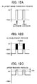
- FIG. 12A illustrates the surface potential of a photoreceptor when the photoreceptor is charged to uniformly have a potential of -700 V and then exposed to imagewise light (i.e., the surface potential of a latent electrostatic image formed on the photoreceptor). In this case, the surface potential of the exposed portion is about 0 V.
- FIG. 12B illustrates the surface potential of the photoreceptor when the latent image is developed with a toner (i.e., the surface potential of the photoreceptor having a toner image thereon) due to the potential difference between the development potential and the surface of the photoreceptor.
- FIG. 12C illustrates the surface potential of the photoreceptor after the toner image is transferred onto a receiving paper while a reverse bias is applied to the receiving paper. In this case, the exposed portions have a certain positive potential (for example, +10 V in FIG. 17C).
- the surface potential (for example, -690 V) of the former image portion is lower than that (i.e., -700 V) of the other portions. If a half-tone image is formed on an area including the former image portion and a former non-image portion, the difference in potential between the former image portion and a non-lighted portion is larger than that between the former non-image portion and the non-lighted portion, and thereby a dense image (a positive image) is formed on the former image portion.
- the residual image problem also occurs in a digital image forming method in which half tone images constituted of digital dot images are formed as widely used in the inkjet printing methods.
- the illuminance in a beam spot formed on a photoreceptor to form a latent dot image thereon is not uniform and has a certain distribution in a direction from the center to the periphery of the beam spot.
- the resultant latent dot image portion has a larger area than the other latent dot image portions because the potential of the latent dot image portion is biased by, for example, +10 V.
- the resultant dot toner image has a larger diameter than that of the dot image in other portions, and thereby the portions of the widened dot image potions are observed to be dense, resulting in formation of a residual positive image. This phenomenon is more apparent in high definition image formation, for example, in image formation with a resolution of 1200 dpi than with a resolution of 600 dpi.
- JOP 10-115946 discloses a photoreceptor having an outermost layer which includes a polyarylate resin and which has a dielectric constant not less than 2.3.
- JOP 11-184135 discloses a photoreceptor having a photosensitive layer including an azo pigment and an outermost layer including a polyarylate resin.
- polyarylate resins have high crystallinity, and therefore can orient the CTM included therein to some extent. It is considered that by orienting the CTM and using the specific azo pigment, the charge injection barrier can be decreased and thereby the photo-memory property of the photoreceptor is diminished.
- JOP 10-177263 discloses that a photoreceptor having a CGL including a phthalocyanine compound and an outermost layer including a bisphenol-based polycarbonate is used for an electrophotographic apparatus having an intermediate transfer medium. It is considered that the effect is produced by the combination of the specific compounds.
- JOP 10-177264 discloses that a photoreceptor having a CGL including a phthalocyanine compound and an outermost layer including a charge transport polymer is used for an electrophotographic apparatus having an intermediate transfer medium. It is considered that the effect is produced by the combination of the specific compounds.
- JOP 10-177269 discloses that a photoreceptor having a CGL including a phthalocyanine compound and either an insulating outermost layer or a semiconductive outermost layer including at least a resistance controlling agent is used for an electrophotographic apparatus having an intermediate transfer medium. It is considered that the effect is produced by the combination of the specific compounds.
- JOP 2000-147803 discloses a photoreceptor in which a polycarbonate copolymer obtained from bisphenol A and a monomer having a specific arylene group is used for the outermost layer thereof such as the CTL. It is discussed in the publication that injection of charges having a reverse polarity from the outermost layer side can be prevented.
- JOP 2001-235889 discloses a photoreceptor having an outermost layer including a surface-treated particulate metal oxide, an alcohol-soluble resin and an alcohol-soluble CTM. It is described in the publication that thermoplastic resins cannot be used as the binder resin of the outermost layer because the resins have insufficient mechanical strength and solvents used for dissolving the resins also dissolve the photosensitive layer. It is considered that use of an alcohol-soluble CTM prevents formation of residual images.
- JOP 2002-6528 discloses a photoreceptor having a photosensitive layer and a protective layer including at least one of an alkali metal element and an alkaline earth metal element. It is described therein that by including such an element in the protective layer, ionic conduction properties can be imparted to the protective layer, and thereby a photoreceptor which has good durability and which does not store residual charges can be provided. It is also described therein that it is possible to reduce the residual charges by including a CTM in the protective layer but the abrasion resistance of the protective layer is weak.
- JOP 2000-75521 discloses a photoreceptor including at least one of a chlorogallium phthalocyanine compound and a hydroxygallium phthalocyanine compound as a CGM and a CTM having a hydrazone skeleton. It is described in the publication that the combination of the specific CGM and CTM can diminish the transfer memory property and photo-memory property of the photoreceptor.
- JOP 2000-105478 discloses a photoreceptor having a photosensitive layer including an azo pigment which is for use in an electrophotographic apparatus using a laser diode emitting light with relatively short wavelength of from 380 to 500 nm as image writing light. It is considered that the azo pigments used therein have relatively weak photo-memory property compared to ⁇ -titanylphthalocyanine.
- JOP 2001-305762 discloses a photoreceptor including a CGM and a CTM, wherein the CTM includes a first compound having a polarizability greater than 70 ⁇ which is calculated by structure optimizing calculation using semiempirical molecular orbital calculation using PM3 parameter and having a dipole moment less than 1.8D which is calculated by the structure optimizing calculation, and a second compound having 50% transmittance at a longer wavelength than the first compound. It is described therein that the second compound absorbs extra light irradiating the photoreceptor, and thereby the photo-memory property of the photoreceptor can be diminished.
- JOP 7-92701 discloses a multi-layered photoreceptor in which an oxytitanium phthalocyanine is included in the CGL and at least two kinds of CTMs are included in the CTL, wherein the difference in oxidation potential between the at least two kinds of CTMs is not greater than 0.04 V. It is considered that by using CTMs having almost the same energy level, hopping of the charge carriers between the CTMs can easily occur and the chance of trapping of charge carriers by the CTMs can be decreased, thereby decreasing the quantity of electrons excited by reverse charging performed by a transfer device, resulting in prevention of occurrence of the residual image problem.
- JOP 08-152721 discloses a photoreceptor which is used for a back-lighting type high speed electrophotographic apparatus in which the exposure-development interval is from 10 to 150 msec, wherein the CTL of the photoreceptor has a charge mobility not less than 1 x 10 -6 cm 2 /V ⁇ sec at an electric field of 2 x 10 6 V/cm. It is described therein that when a photoreceptor has a low dynamic photosensitivity, the latent image formation cannot be completed before the start of the developing operation and thereby the potential of the former image portions is increased after repeated use; but by using the technique mentioned above, the dynamic photosensitivity can be improved and thereby the residual image problem can be solved.
- JOP 10-177262 discloses a photoreceptor which is for use in electrophotographic apparatus having an intermediate transfer medium and which has a CGL including a phthalocyanine compound and a CTL including a compound selected from triphenylamine compounds and N,N,N',N'-tetraphenylbenzidine compounds. It is considered that the effect is produced by the combination of the specific compounds.
- JOP 06-313972 discloses a photoreceptor in which the thickness of the CGL is increased so as to be not less than 25 ⁇ m or the content of a CGM in the CGL is increased so as to be not less than 50 % by weight so that a number of charge carriers are trapped in the CGL, to make the resultant ghost image inconspicuous.
- JOP 10-69104 discloses a multi-layered photoreceptor having a CGL including a triarylamine compound having a xylyl group. It is described in the publication that a barrier to carrier transportation is formed at the interface between the CGL and CTL, and charge carriers are trapped thereby. Since the trapped carriers decrease the space electric field in the CGL, the potential of a half-tone image portion is not decreased, and thereby a residual image is formed at the portion.
- a CTM i.e., a triarylamine compound having a xylyl group
- the generated carriers are rapidly injected into the CTL and transported therethrough, and thereby accumulation of trapped carriers (i.e., occurrence of the residual image problem) can be prevented.
- JOP 10-186696 discloses a photoreceptor having an electroconductive substrate 101 and at least a photosensitive layer and a protective layer located overlying the substrate 101 in this order, wherein the photosensitive layer includes oxytitanium phthalocyanine having an Cu K ⁇ X-ray diffraction spectrum in which strong peaks are observed at Bragg (2 ⁇ ) angles of 9.5°, 24.1° and 27.3°. It is considered that the effect can be produced by the specific compound.
- JOP 2002-107972 discloses a photoreceptor having a CGL including a hydroxygallium phthalocyanine compound and a butyral resin which serves as the binder resin and which has an acetal group, an acetyl group and a hydroxyl group, wherein the butyral resin has a butyralation degree not less than 62 % by mole, a weight average molecular weight (Mw) not less than 2.0 x 10 5 and a number average molecular weight not less than 5.0 x 10 4 . It is considered that the number of photo-carriers can be reduced by the specific polyvinyl butyral, and thereby occurrence of the residual image problem can be prevented.
- JOP 07-43920 discloses a multi-layered photoreceptor in which a specific azo pigment is used for the CGL and a CTM having a fluorene skeleton is used for the CTL. It is considered that addition of the specific compounds prevents the photoreceptor from suffering light fatigue. It is considered that the effect can be produced by the specific compound.
- JOP 09-211876 discloses a negative polarity-type photoreceptor having a high ⁇ property, in which a CGL including a phthalocyanine compound and a p-type CTL including a material selected from the group consisting of inorganic p-type semiconductors and particulate t-Se and charge transport polymers are used. It is described therein that the p-type CTL is characterized by including no positive hole transport material and thereby diffusion of a positive hole transport material into the CGL can be prevented. Therefore, trapping caused by the phthalocyanine pigment can be prevented and thereby the residual image problem can be prevented.
- JOP 08-22136 discloses a photoreceptor having an undercoat layer including a silane coupling agent and an inorganic filler. It is described therein that by forming such an undercoat layer, charges to be flown to the substrate 101 are smoothly flown to the substrate 101, and thereby occurrence of the residual image problem can be prevented.
- JOP 11-184127 discloses a photoreceptor having an undercoat layer including a resin having a specific polyamide acid or polyamide acid ester structure or a polyimide structure, and a resin having a cyanoethyl group. It is considered that by using such resins, the photoreceptor is prevented from suffering light fatigue.
- JOP 2000-112162 discloses a photoreceptor having an undercoat layer including a crosslinking resin which hardly changes its resistance even when the environmental humidity changes. It is described therein that JOP 08-146639 discloses an undercoat layer including a polycyclic quinone, perylene, etc.; JOP 10-73942 discloses an undercoat layer including a metallocene compound, an electron accepting compound and a melamine resin; JOP 08-22136 discloses an undercoat layer including a particulate metal oxide and a silane coupling agent; and JOP 09-258469 discloses an undercoat layer including a particulate metal oxide having a surface treated with a silane coupling agent.
- JOP 2000-112162 proposes to use a combination of a polyamide resin and a zirconium compound or a combination of a polyamide resin, a zirconium alkoxide and a diketone compound such as acetyl acetone for the undercoat layer.
- JOP 2001-51438 proposes to use a combination of a cellulose resin, a zirconium compound, a zirconium alkoxide, and a diketone compound for the undercoat layer.
- JOP 2001-305763 discloses a photoreceptor having an undercoat layer, including a CGM and a CTM, wherein the CTM includes a material having a polarizability greater than 70 ⁇ which is calculated by structure optimizing calculation using semiempirical molecular orbital calculation using PM3 parameter and having a dipole moment less than 1.8D which is calculated by the structure optimizing calculation, and a specific arylamine compound, wherein the undercoat layer includes a particulate titanium oxide treated with an organic silicon compound and a polyamide having a specific diamine component as a constituent. It is considered in the publication that by forming such an undercoat layer, the carriers remaining in the photosensitive layer can be easily transported.
- JOP 2002-107983 discloses a system in which the undercoat layer of the photoreceptor has a volume average resistivity of from 10 10 to 10 12 ⁇ ⁇ cm, the CTL thereof has a thickness not greater than 18 ⁇ m and the electrophotographic apparatus does not include a quencher. It is considered that by not using a quencher, the photoreceptor is prevented from suffering light fatigue, and since the undercoat layer has a proper resistance, injection of charges from the substrate 101 to the photosensitive layer can be suppressed, resulting in prevention of accumulation of space charges in the photoreceptor.
- JOP 10-177261 discloses a photoreceptor for use in an electrophotographic apparatus having an intermediate transfer medium, wherein the photoreceptor has a CGL including a phthalocyanine compound and an outermost layer including a material having a hindered phenol structure. It is considered that the effect is produced by the specific material.
- JOP 2000-292946 discloses a photoreceptor having a CGL including a phthalocyanine pigment and a dithiobenzyl compound. It is described therein that by using such materials, the photo-memory property of the photoreceptor can be diminished and thereby occurrence of the positive-ghost problem can be prevented.
- JOP 07-13374 proposes a technique in that the photoreceptor used is sometimes charged reversely so as to have a reverse (positive) charge, and then allowed to settle.
- a photoreceptor having a high sensitive CTL In a photoreceptor having a high sensitive CTL, a large number of charge carriers are induced by light irradiation. In this case, electrons whose number is the same as that of the holes injected to the CTL are formed. If the electrons are not discharged to the substrate 101, the electrons remain in the CGL and thereby the residual image problem tends to occur.
- a photoreceptor is reversely (i.e., positively) charged, electrons are injected from the substrate 101 and electron traps are formed in the CGL.
- difference in the number of electron traps between the lighted portions and unexposed portions is little, and thereby the ghost image becomes inconspicuous.
- JOP 07-44065 discloses a technique in that a DC voltage overlapped with an AC voltage is applied to the substrate 101 of the photoreceptor. By applying a reverse bias to the substrate 101, electrons trapped in the CGL can be discharged therefrom. By overlapping an AC voltage, the electric current can be increased and thereby the reverse charge bias effect can be accelerated.
- JOP 10-123802 discloses a technique in that charging (not main charging) is performed on a multi-layered photoreceptor having a CGL including a phthalocyanine compound and then light discharging is performed thereon, wherein the main charging is performed thereon if the predetermined portion of the photoreceptor reaches the main charging portion. It is described therein that by performing such an image forming method, the photoreceptor is charged after the space charges in the photoreceptor are released therefrom, and thereby occurrence of the residual image problem can be prevented.
- JOP 10-123855 discloses a technique in that a controller is provided in an electrophotographic apparatus, which controls the transfer current flowing from a transfer device to the multi-layered photoreceptor used, wherein the photoreceptor has a CGL including a phthalocyanine compound. It is described therein that the greater the transfer current, the more conspicuously a negative residual image is formed. The reason is considered as follows. When an image is transferred, holes are injected into non-lighted portions of the photoreceptor and the holes are trapped at the interface of the CGL or the CTL on the substrate 101 side. The trapped holes are released in the next charging process, and thereby the dark decay is enhanced (i.e., apparent sensitization), resulting in occurrence of formation of a negative residual image. Therefore, by controlling the transfer current, the number of charge carriers injected into the photoreceptor can also be controlled and occurrence of the residual image problem can be prevented.
- JOP 2000-231246 proposes a technique in that the wavelength of the image writing light and the discharging light are determined depending on the ratio of photo-memory property before charging to the photosensitivity of the photoreceptor.
- JOP 10-123856 proposes a technique in that light irradiation is performed on a photoreceptor having a CGL including a phthalocyanine compound before the transfer process to decrease the potential of the unexposed portion to 1/3 of the potential, in order to prevent occurrence of the residual image problem. It is considered that by performing such irradiation, the difference in potential between the exposed portion and the unexposed portion is reduced and thereby the residual image becomes inconspicuous.
- JOP 10-246997 discloses a technique in that in an electrophotographic apparatus using a photoreceptor having a photosensitive layer and a protective layer including a light-curable acrylic resin, a humidity sensor is provided in the vicinity of the photoreceptor to change the current of the AC component of the voltage applied by the charger depending on the humidity. It is described therein that by using such a technique, chance of formation of blurred images can be decreased. In addition, it is described therein that the photo-memory property of the photoreceptor is weakened using the technique, but the mechanism thereof is not described therein.
- JOP 2001-117244 discloses a technique in that in order to prevent formation of ghost images when a S-form photoreceptor is used, the period of half-decay of the potential on the photoreceptor in light irradiation, which period is determined using a Xerographic Time Of Flight (TOF) method, is controlled so as to be not greater than 1/10 of the exposure-development interval between the light irradiation process and the following development process.
- TOF Time Of Flight
- JOP 2002-107983 discloses a technique in that by not using a quencher, the photoreceptor is prevented from suffering light fatigue.
- JOP 2002-123067 discloses a technique in that the photoreceptor and charging conditions are controlled so as to satisfy the following relationship:
- an object of the present invention is to provide an electrophotographic photoreceptor capable of producing high quality images at a high speed which is achieved by good durability, good cleanability and good transferability while obviating the residual image problem.
- Another object of the present invention is to provide a method of manufacturing such a photoreceptor.
- Yet another object of the present invention is to provide an image forming apparatus and a process cartridge which can produce high quality images at a high speed without causing the residual image problem and without frequently changing the photoreceptor.
- an electrophotographic photoreceptor (1; 11; 21; 31; 51; 71) including a conductive substrate 101, an undercoat layer 104 located overlying the conductive substrate 101, a photosensitive layer located overlying the undercoat layer 104.
- the photosensitive layer contains a charge generation layer 102 located overlying the undercoat layer 104 and a charge transport layer 103 located overlying the charge generation layer 102.
- the charge generation layer 102 when the charge generation layer 102 is irradiated with light having a highest reflectivity for the charge generation layer 102 in a range of from 360 nm to 740 nm after the undercoat layer 104 and the charge generation layer 102 are formed overlying the conductive substrate 101, the charge generation layer 102 has a reflectivity of from 15 to 21 %.
- the charge generation layer 102 contains a disazo pigment represented by the following formula (1)
- the charge generation layer 102 has a reflectivity of from 17 to 19 %.
- an electrophotographic apparatus (100; 200; 300; 400; 500; 600) which contains the electrophotographic photoreceptor (1; 11; 21; 31; 51; 71) mentioned above, a charger (2; 12; 22; 32; 52; 72) configured to uniformly charge the surface of the photoreceptor (1; 11; 21; 31; 51; 71), an image irradiator (3; 13; 23; 33; 53; 73) configured to irradiate the uniformly charged electrophotographic photoreceptor (1; 11; 21; 31; 51; 71) with light to form a latent electrostatic image thereon, a developing device (4; 14; 24; 34; 54; 74) configured to develop the latent electrostatic image with a toner 5, a transfer device (6, 16; 26; 36; 46; 56; 76) configured to transfer the developed image to a receiving material (8; 28; 38; 58; 78) and a cleaner (7; 17; 27; 37; 57; 77) configured to remove
- the electrophotographic photoreceptor (1; 11; 21; 31; 51; 71) further satisfies the following relationship: 12 (V/ ⁇ m) ⁇ electric field intensity (V/D) ⁇ 35 (V/ ⁇ m), wherein D ( ⁇ m) represents a thickness of the charge transport layer 103 of the electrophotographic photoreceptor (1; 11; 21; 31; 51; 71) and V (V) represents an absolute potential of the surface of the electrophotographic photoreceptor (1; 11; 21; 31; 51; 71) due to charging.
- the electrophotographic apparatus contains an electrophotograpnic photoreceptor (1; 11; 21; 31; 51; 71) having a charge generation layer 102 including the disazo pigment (I) and having a light transmittance of from 35 to 65 % against light to form a latent electrostatic image on the electrophotographic photoreceptor (1; 11; 21; 31; 51; 71) .
- the electrophotographic photoreceptor (1; 11; 21; 31; 51; 71) satisfies the following relationship: 15 (V/ ⁇ m) ⁇ electric field intensity (V/D) ⁇ 32 (V/ ⁇ m).
- the toner 5 for use in developing the latent electrostatic image has a sphere form.
- the electrophotographic apparatus (100; 200; 300; 400; 500; 600) mentioned above further contains an intermediate transfer device (40; 80) to which multiple separate color toner images developed on the electrophotographic photoreceptor (1; 11; 21; 31; 51; 71) with separate color toners are transferred in a first step to form an overlaid color toner image on the intermediary transfer device (40; 80) while overlaying the separate color images thereon and from which the overlaid color toner image is transferred in a second step to the receiving material (8; 28; 38; 58; 78).
- an intermediate transfer device 40; 80
- the charge generation layer 102 includes a disazo pigment represented by the following formula (1).
- a process cartridge 300 which includes the electrophotographic photoreceptor (1; 11; 21; 31; 51; 71) mentioned above, optionally an image irradiator (3; 13; 23; 33; 53; 73) configured to irradiate the uniformly charged electrophotographic photoreceptor (1; 11; 21; 31; 51; 71) with light to form a latent electrostatic image thereon, and at least one of preferably all of the following devices: a charger (2; 12; 22; 32; 52; 72) configured to uniformly charge a surface of the electrophotographic photoreceptor (1; 11; 21; 31; 51; 71); a developing device (4; 14; 24; 34; 54; 74) configured to develop the latent electrostatic image with a toner 5; a transfer device (6, 16; 26; 36; 46; 56; 76) configured to transfer the developed image to a receiving material(8; 28; 38; 58; 78); a cleaner (7; 17; 27; 37; 57
- a method of manufacturing the photoreceptor (1; 11; 21; 31; 51; 71) mentioned above includes the steps of forming the conductive substrate 101, the undercoat layer 104 located overlying the conductive substrate 101, forming a charge generation layer 102 located overlying the undercoat layer 104 and a charge transport layer 103 located overlying the charge generation layer 102.
- an electrophotographic apparatus producing a high density image with a high speed often causes the residual image problem but occurrence of the residual images can be effectively restrained by using an electrophotgraphic photoreceptor having a specific reflectivity or a specific light transmittance in the irradiation light wavelength band of the photoreceptor and a specific range electric field intensity (V/D), wherein D ( ⁇ m) is a thickness of the CTL 102 of the photoreceptor and V(V) is an absolute voltage of the surface of the photoreceptor due to charging, and further made of a disazo pigment having a specific structure.
- V/D specific range electric field intensity
- an electrophotographic photoreceptor having a multi-layer structure has side effects such as deterioration in sensitivity and voltage rise at an exposed portion when the reflectivity of the CGL 102 against light having the highest reflectivity therefor is raised or when the light transmittance of the CGL 102 against light having a wavelength of the image irradiation light source is lowered, namely the thickness of the CGL 102 is thin.
- the reason why the wavelength having the highest reflectivity is used is that it is easy to determine and control.
- the inventors of the present invention have discovered that a disazo pigment can effectively restrain these side effects.
- Azo pigments are generally prepared by reacting an aromatic diazonium salt and a coupling component (coupler) in the presence of a salt.
- a coupling component coupled to a salt.
- azo pigments having at least two azo groups such as disazo pigments or trisazo pigments are typically used as CGM.
- the structure of these azo pigments greatly affects electrostatic characteristics such as sensitivity.
- azo pigments For these azo pigments, naphthol based couplers are greatly preferred in terms of sensitivity. However, the sensitivity varies depending on the state of particles of an azo pigment used as CGM for an electrophotographic photoreceptor.
- the disazo pigments represented by the formula (I) for use in the present invention i.e., the disazo pigments having a coupler remaining group represented by the following formulae (II) to (VIII)
- the particle state of the disazo pigments achieved when a layer of the disazo pigments is formed on an electrophotographic photoreceptor is extremely stable. Due to these factors, a photoreceptor made of these disazo pigments has excellent initial sensitivity, excellent maintainabiliy and excellent light resistance.
- the bond in formulae (II) between coupler and azo group can be in any position to X 1 or Y 1 , but is preferably in ortro position to X1.
- the substituted or non-substituter alkyl group preferably is an alkyl group comprising 1 to 20 carbon atoms, more preferably 1 to 10 carbon atoms, and most preferably 1 to 4 carbon atoms. Suitable examples are methyl, ethyl, propyl, butyl, pentyl, vinyl, allyl, cyclohexyl, cycloheptyl, 2-ethyl hexyl amongst others.
- the substituted or non-substituter aryl group preferably is an aryl group comprising 6 to 18 carbon atoms, more preferably 6 to 14 carbon atoms, and most preferably 6 to 10 carbon atoms. Suitable examples are benzene, naphthalene, anthracene, phenantrene, fluorine (fluorene) and the like.
- the substituted or non-substituter aralkyl group preferably comprises 6 to 18 carbon atoms in the aryl group and 1 to 10 carbon atoms in the alkylene group, more preferably 6 to 10 carbon atoms in the aryl group and 1 to 4 carbon atoms in the alkylene group.
- Suitable examples are phenylmethyl and diphenyl methyl.
- the substituted or non-substituted heterocyclic group preferably comprises from 2 to 20 carbon atoms, more preferably 2 to 10 carbon atoms, and 1 to 3, preferably 1 hetero atom(s) selected from the group, consisting of nitrogen, sulfur and oxygen.
- the hetero atom(s) is/are nitrogen or oxygen.
- Suitable examples are furane, thiophene, pyrroline, oxazole, thiazole, pyrazole, isooxazole, imidazole, benzofurane, indole, benzoxazole, benzothiazole, benzimidazole, carbazole, morpholine, pyridine, chinoline, acridine, pyrimidine, pyrazine, pyrane, ⁇ -chromene, and xanthene.
- the substituted or non-substituted aromatic hydrogarbon groups Ar 1 and Ar 2 preferably have about 6 to 30 carbon atoms, preferably 6 to 14 carbon atoms and most preferably 6 to 10 carbon atoms. It can be any of the groups listed above for the aryl and aralkyl groups.
- Ar 1 or Ar 2 are phenyl or phenylmethyl.
- an electrophotographic apparatus capable of producing quality images at a high speed can be obtained.
- the reflectivity by specifying a reflectivity of a CGL 102 measured by a spectrophotometric colorimeter in a range of from 360 nm to 740 nm after an undercoat layer 104 and the CGL 102 are formed, a stable value is obtained regardless of the specification such as kind and thickness of a CTL 102 overlaid on the CGL 102.
- the amount of the CGL 102 attached can be determined and thus coating conditions for the CGL 102 can be controlled by feedback in the coating processes.
- a photoreceptor having a high reflectivity against light having the highest reflectivity at the CGL is good or a photoreceptor having a thin CGL 102 (i.e., the light emittance in the irradiation light wavelength band is high) is good.
- the reflectivity or the light transmittance is too high, optical decay characteristics deteriorate and a potential at an exposed portion rises.
- the reflectivity or the light transmittance is high and the photoreceptor is repetitively used while the electric field intensity is high, electrostatic stresses on the photosensitive layer increase, resulting in accumulation of light fatigue. Thus residual images tend to occur in this case. It is important to control the electric field intensity within a low range.
- Fig. 1 is a schematic diagram illustrating an embodiment of the electrophotographic apparatus of the present invention and variations thereof described later are also within the scope of the present invention.
- a photoreceptor 1 is an electrophotographic photoreceptor satisfying the requirements of the present invention.
- the photoreceptor 1 has a drum form, but photoreceptors having a form such as sheet-form and endless belt-form can also be used.
- a discharging lamp 10 to decrease charges remaining on the photoreceptor 1 a charger 2 configured to charge the photoreceptor 1, an imagewise light irradiator 3 configured to irradiate the photoreceptor 1 with imagewise light to form an electrostatic latent image on the photoreceptor 1, an image developing device 4 configured to develop the latent image with a toner 5 to form a toner image on the photoreceptor 1, and a cleaner 7 including a cleaning blade configured to clean the surface of the photoreceptor 1 are arranged in contact with or in close piximity to the photoreceptor 1.
- the toner image formed on the photoreceptor 1 is transferred on a receiving material 8 (e.g., receiving paper) by a transfer device 6.
- the toner image on the receiving material 8 is fixed thereon by a fixer 9.
- any known chargers such as corotrons, scorotrons, solid state chargers, and roller chargers can be used.
- contact chargers and short-range chargers are preferably used in terms of power consumption.
- short-range chargers which can charge a photoreceptor while a proper gap is formed between the chargers and the surface of the photoreceptor are more preferably used.
- the above-mentioned known chargers can be used.
- a combination of a transfer charger and a separating charger is preferably used.
- Suitable light sources for use in the imagewise light irradiator 3 and the discharging lamp 10 include fluorescent lamps, tungsten lamps, halogen lamps, mercury lamps, sodium lamps, light emitting diodes (LEDs), laser diodes (LDs), light sources using electroluminescence (EL), and the like.
- LEDs light emitting diodes
- LDs laser diodes
- EL electroluminescence
- filters such as sharp-cut filters, band pass filters, near-infrared cutting filters, dichroic filters, interference filters, color temperature converting filters and the like can be used.
- Suitable cleaners for use as the cleaner 7 include cleaning blades made of a rubber, fur brushes and mag-fur brushes.
- an electrostatic latent image having a positive (or negative) charge is formed on the photoreceptor 1.
- a positive image can be obtained.
- a negative image i.e., a reversed image
- known developing methods can be used.
- discharging methods known discharging methods can also be used.
- Fig. 2 is a schematic view illustrating another embodiment of electrophotographic process of the present invention.
- the photoreceptor 1 is an electrophotographic photoreceptor satisfying the requirements of the present invention and has a belt form.
- the belt-form photoreceptor 11 is rotated by rollers R1 and R2.
- the photoreceptor 11 is charged with a charger 12, and then exposed to imagewise light emitted by an imagewise light irradiator 13 to form an electrostatic latent image on the photoreceptor 11.
- the latent image is developed with an image developing device 14 to form a toner image on the photoreceptor 11.
- the toner image is transferred onto a receiving paper (not shown) using a transfer device 16.
- the surface of the photoreceptor 11 is cleaned with a cleaning brush 17 after performing a pre-cleaning light irradiating operation using a pre-cleaning light irradiator 18. Then the photoreceptor 11 is exposed to light emitted by a discharging light source 19 to reduce the charge remaining thereon.
- the pre-cleaning light irradiating process light irradiates the photoreceptor 11 from the side of the substrate 101 thereof. In this case, the substrate 101 has to be light-transmissive.
- the elecctrophotographic processes for use in the present invention is not limited to the processes shown in FIGS. 1 and 2.
- the pre-cleaning light irradiating operation can be performed from the photosensitive layer side of the photoreceptor 11.
- the light irradiation in the imagewise light irradiating process and the discharging process may be performed from the substrate 101 side of the photoreceptor 11.
- a pre-transfer light irradiation operation which is performed before transferring the toner image
- a preliminary light irradiation operation which is performed before the imagewise light irradiation, and other light irradiation operations may also be performed.
- the above-mentioned image forming unit may be fixedly set in an electrophotographic apparatus such as copiers, facsimile machines and printers.
- the image forming unit can be set therein as a process cartridge.
- the process cartridge means an image forming unit which includes a photoreceptor and at least one or more or all of a charger, an imagewise light irradiator, an image developing device, a transfer device, a cleaner, and a queencher.
- FIG. 3 An embodiment of the process cartridge of the present invention is illustrated in FIG. 3.
- the process cartridge includes a photoreceptor 21, which is the photoreceptor of the present invention, a charger 22 configured to charge the photoreceptor 21, an image developing device (a developing roller) 24 configured to develop an electrostatic latent image, which is formed on the photoreceptor by an imagewise light irradiator 23, with a toner to form a toner image, a transfer device 26 configured to transfer the toner image to a receiving material 28, and a cleaning blade 27 configured to clean the surface of the photoreceptor 21.
- Numerals 29 and 30 denote a fixer and a quencher, respectively.
- the photoreceptor 21 has a drum form, but photoreceptors having a form such as sheet-form and endless belt-form can also be used.
- FIG. 4 illustrates another embodiment of the electrophotographic apparatus of the present invention.
- the electrophotographic apparatus has a photoreceptor 31 which is the photoreceptor of the present invention.
- a charger 32 Around the photoreceptor 31, a charger 32, an imagewise light irradiator 33, an image developing unit 34 having a black image developing device 34Bk, a cyan image developing device 34C, a magenta image developing device 34M and a yellow image developing device 34Y, an intermediate transfer belt 40 serving as an intermediate transfer medium, and a cleaner 37 are arranged.
- the image developing devices 34Bk, 34C, 34M and 34Y can be independently controlled, and each of the image developing devices is independently driven when desired.
- Toner images formed on the photoreceptor 31 are transferred onto the intermediate transfer belt 40 by a first transfer device 36.
- the intermediate transfer belt 40 is brought into contact with the photoreceptor 31 by the first transfer device 36 only when a toner image on the photoreceptor 31 is transferred thereto.
- the toner images overlaid on the intermediate transfer belt 40 are transferred onto a receiving material 38 by a second transfer device 46, and the toner images are fixed on the receiving material 38 by a fixer 39.
- the second transfer device 46 is brought into contact with the intermediate transfer belt 40 only when the transfer operation is performed.
- each toner image is formed on the intermediate transfer belt and the overlaid toner images are transferred onto a receiving material. Therefore, an image can be formed on any kinds of receiving materials.
- the image forming method using an intermediate transfer medium can be applied to the electrophotographic apparatus as illustrated in FIGS. 1-3, and 5 as well as the electrophotographic apparatus illustrated in FIGS. 4 and 6.
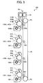
- FIG. 5 illustrates another embodiment of the electrophotographic apparatus of the present invention.
- the electrophotographic apparatus has four color image forming sections, i.e., yellow, magenta, cyan and black image forming sections.
- the image forming sections include respective photoreceptors 51Y, 51M, 51C and 51Bk.
- the photoreceptor 51 for use in the electrophotographic apparatus satisfies the requirements of the present invention.
- a charger (52Y, 52M, 52C or 52Bk), an imagewise light irradiator (53Y, 53M, 53C or 53Bk), an image developing device (54Y, 54M, 54C or 54Bk), and a cleaner (57Y, 57M, 57C or 57Bk) are arranged.
- a feed/transfer belt 60 which is arranged below the image forming sections, is tightly stretched by rollers R3 and R4.
- the feed/transfer belt 60 is attached to or detached from the photoreceptors 51 by transfer devices 56Y, 56M, 56C and 56Bk to transfer toner images from the photoreceptors 51 to a receiving material 58.
- the resultant color toner image is fixed by a fixer 59.
- the tandem-type electrophotographic apparatus illustrated in FIG. 5 has a plurality of photoreceptors 51 for forming four color images, and color toner images which can be formed in parallel can be transferred onto the receiving material 58. Therefore, the electrophotographic apparatus can form full color images at a much higher speed than that of such an electrophotographic apparatus as illustrated in FIG. 4.
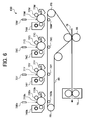
- FIG. 6 illustrates another embodiment of the electrophotographic apparatus of the present invention, which is a tandem-type color electrophotographic apparatus having an intermediate transfer medium.
- the electrophotographic apparatus has four color image forming sections, i.e., yellow, magenta, cyan and black image forming sections.
- the image forming sections include respective photoreceptors 71Y, 71M, 71C and 71Bk.
- the photoreceptors 71 for use in the electrophotographic apparatus satisfy the requirements of the present invention.
- each of the photoreceptors (71Y, 71M, 71C or 71Bk), a charger (72Y, 72M, 72C or 72Bk), an imagewise light irradiator (73Y, 73M, 73C or 73Bk), an image developing device (74Y, 74M, 74C or 74Bk), and a cleaner (77Y, 77M, 77C or 77Bk) are arranged.
- an intermediate transfer belt 80 which is arranged below the image forming sections, is tightly stretched by rollers R5 and R6 and other rollers.
- the intermediate transfer belt 80 is attached to or detached from the photoreceptors by transfer devices 76Y, 76M, 76C and 76Bk to receive toner images from the photoreceptors.
- the color toner images formed on the intermediate transfer belt 80 are transferred onto a receiving material 78 at once by a transfer device 86. Then the color toner images are fixed by a fixer 79.
- FIG. 7 illustrates a schematic cross section of an embodiment of the photoreceptor having the layer structure of the present invention.
- the photoreceptor has an electroconductive substrate 101 , a charge generation layer 102 (CGL 102) 102 and a charge transport layer 103 (CTL 102) 103.
- CGL 102 charge generation layer 102
- CTL 102 charge transport layer 103
- FIG. 8 illustrates a schematic cross section of another embodiment of the photoreceptor having the layer structure of the present invention.
- the photoreceptor has a structure such that an undercoat layer 104 is formed between the substrate 101 and the CGL 102 of FIG. 7.
- Suitable materials for use as the electroconductive substrate 101 include materials having a volume resistance not greater than 10 10 ⁇ ⁇ cm. Specific examples of such materials include plastic or paper cylinders or films, on the surface of which a metal such as aluminum, nickel, chromium, nichrome, copper, gold, silver, platinum, iron and the like, or a metal oxide such as tin oxides, indium oxides and the like, is formed by a method such as vapor deposition and sputtering. In addition, a plate of a metal such as aluminum, aluminum alloys, nickel and stainless steel can be used.
- a metal cylinder can also be used as the substrate 101, which is prepared by tubing a metal such as aluminum, aluminum alloys, nickel and stainless steel by a method such as drawing, impact molding, extrusion molding, extrusion drawing or cutting, and then subjecting the surface of the tube to cutting, super finishing, polishing and the like treatments.
- the photosensitive layer of the present invention is a multi-layered photosensitive layer having the CGL 102 on the electroconductive substrate 101 and the CTL 102 103 over laid on the CGL 102.
- the structures of each layer of this multi-layered photosensitive layer are now described.
- the CGL 102 includes a CGM as a main component, and optionally includes a binder resin.
- a disazo pigment represented by formula (I) described before is a disazo pigment represented by formula (I) described before.
- disazo pigments include a compound having a benzene ring substituent having Cl at the ortho position at each end of the compound such as (2,7-bis[3-(2-chlorophenyl)carbamoyl-2-hydroxy-1-naphthylazo]-9-fluorenone.
- Specific suitably preferred examples among the compounds represented by formula (I) is a disazo pigment having the structure represented by the following formula (1).
- CGMs can be used alone or in combination.
- Suitable binder resins which are optionally included in the CGL 102, include polyamide, polyurethane, epoxy resins, polyketone, polycarbonate, polyarylate, silicone resins, acrylic resins, polyvinyl butyral, polyvinyl formal, polyvinyl ketone, polystyrene, poly-N-vinylcarbazole, polyacrylamide, and the like resins.
- charge transport polymers can be used as the binder resin of the CGL 102.
- low molecular weight CTMs can be added to the CGL 102 if desired.
- the CTMs are classified into positive-hole transport materials and electron transport materials and further classified into low molecular weight CTMs and charge transport polymers.
- the electron transport materials include electron accepting materials such as chloranil, bromanil, tetracyanoethylene, tetracyanoquinodimethane, 2,4,7-trinitro-9-fluorenon, 2,4,5,7-tetranitro-9-fluorenon, 2,4,5,7-tetanitroxanthone, 2,4,8-trinitrothioxanthone, 2,6,8-trinitro-4H-indeno[1,2-b]thiophene-4-one, 1,3,7-trinitrodibenzothiophene-5,5-dioxide, and the like.
- electron accepting materials such as chloranil, bromanil, tetracyanoethylene, tetracyanoquinodimethane, 2,4,7-trinitro-9-fluorenon, 2,4,5,7-tetranitro-9-fluorenon, 2,4,5,7-tetanitroxanthone, 2,4,8-trinitrothioxanthone, 2,6,8-trinitro-4H-indeno[1,2-
- These electron transport materials can be used alone or in combination.
- positive-hole transport materials include oxazole derivatives, oxadiazole derivatives, imidazole derivatives, triphenyl amine derivatives, 9-(p-diethylaminostyrylanthracene), 1,1-bis-(4-dibenzylaminophenyl)propane, styryl anthracene, styryl pyrazoline, phenyl hydrazone, ⁇ -phenyl stilbene derivatives, thiazole derivatives, triazole derivatives, phenazine derivatives, acridine derivatives, benzofuran derivatives, benzimidazole derivatives, thiophene derivatives, etc.
- the positive-hole transport materials can be used alone or in combination.
- Suitably preferred methods for forming the CGL 102 include casting methods from a solution dispersion system.
- the casting methods for forming the CGL 102 typically include the following steps:
- the thickness of the CGL 102 formed as mentioned above satisfies the following conditions: the reflectivity of the CGL 102 against light having a wavelength showing the highest reflectivity therefor when measured by a spectrophotometric colorimeter in the range of from 360 nm to 740nm after an undercoat layer 104 and the CGL 102 are formed is from 15 to 21 % and preferably from 17 to 19 %; and/or light transmittance of the CGL 102 against light having a wavelength used in the image irradiation is from 35 to 65 % and preferably from 40 to 55 %.
- the CGL 102 When the light transmittance is too low (i.e., the CGL 102 is formed thick enough to reduce the light transmittance), characteristics such as optical decay, namely, photosensitivity, are excellent in most cases but charging stability tends to be bad and therefore deteriorates for repeated uses in a dark place. In addition, such a photoreceptor tends to be vulnerable to reversed bias at a transfer portion. Thereby when the photoreceptor is recharged, a potential difference occurs between the portion which is irradiated by an irradiator and the portion which is not. Consequently, a residual image is obtained at a half tone portion having a dense writing.
- the amount of the CGL 102 attached namely, to have an undercoat layer 104 and a CGL 102 having a high reflectivity against light having a wavelength showing the highest reflectivity at the CGL 102 and/or to have a thin CGL 102 (i.e., the light transmittance in the wavelength band of the irradiation light is high).
- the reflectivity and/or light transmittance is too high, optical decay characteristics deteriorate and a potential at an exposed portion rises.
- the CTL 102 103 is typically prepared by preparing a CTL 102 coating liquid in which a mixture of a CTM and a binder resin or a charge transport polymer material is dissolved or dispersed in a solvent, and then coating the coating liquid followed by drying.
- polymers for use as the binder resin of the CTL 102 include thermoplastic resins and thermosetting resins such as polystyrene, styrene / acrylonitrile copolymers, styrene / butadiene copolymers, styrene / maleic anhydride copolymers, polyester, polyvinyl chloride, vinyl chloride / vinyl acetate copolymers, polyvinyl acetate, polyvinylidene chloride, polyarylate, polycarbonate, cellulose acetate resins, ethyl cellulose resins, polyvinyl butyral, polyvinyl formal, polyvinyl toluene, acrylic resins, silicone resins, fluorine-containing resins, epoxy resins, melamine resins, urethane resins, phenolic resins and alkyd resins, but are not limited thereto.
- thermoplastic resins and thermosetting resins such as polystyrene, styren
- polystyrene resin can be used alone or in combination.
- copolymers of the monomers of the polymer materials mentioned above can also be used.
- copolymers of the monomers with a CTM can also be used.
- resins such as polyester, polycarbonate, acrylic resins, polystyrene, polyvinylidene chloride, polyethylene, polypropylene, fluorine-containing resins, polyacrylonitrile, acrylonitrile / styrene / butadiene copolymers, acrylonitrile / styrene copolymers and ethylene / vinyl acetate copolymers are preferably used.
- Electrically inactive charge transport polymer materials mean polymers which do not have a structure having a photoconductive property, such as the triarylamine structure.
- the content thereof is preferably not greater than 50 % by weight of the sum of additive and binder in view of photosensitivity of the resultant photoreceptor.
- CTMs for use in the CTL 102 include the low molecular weight electron transport materials, low molecular weight positive hole transport materials, and charge transport polymer materials mentioned above.
- the content thereof is from 40 to 200 parts by weight, and preferably from 70 to 150 parts by weight, per 100 parts by weight of the resin components included therein.
- the content thereof is from 0 to 500 parts by weight, and preferably from 0 to 150 parts by weight, per 100 parts by weight of the charge transport components included therein.
- the difference in ionization potential between the two or more kinds of CTMs is as small as possible, specifically the difference is preferably not greater than 0.15 eV. In this case, it is prevented that one of the CTMs serves as a trap of the other CTMs.
- the content of the CTMs in the CTL 102 is preferably not less than 70 parts by weight per 100 parts by weight of the resin components in the CTL 102.
- Suitable solvents for use in the CTL 102 coating liquid include ketone such as methyl ethyl ketone, acetone, methyl isobutyl ketone, and cyclohexanone; ethers such as dioxane, tetrahydrofuran, and ethyl cellosolve; aromatic solvents such as toluene, and xylene; halogen-containing solvents such as chlorobenzene, and dichloromethane; esters such as ethyl acetate and butyl acetate; etc. These solvents can be used alone or in combination.
- the CTL 102 can include one or more additives such as antioxidants, plasticizers, lubricants and ultraviolet absorbents, if desired. Specific examples thereof are mentioned below. These additives are added in the CTL 102 in an amount of from 0.1 to 50 parts by weight, preferably from 0.1 to 20 parts by weight, per 100 parts by weight of the resin components therein. The leveling agents are added in an amount of from 0.001 to 5 parts by weight per 100 parts by weight of the resin components therein.
- Suitable coating methods for use in coating the CTL 102 coating liquid include dip coating methods, spray coating methods, ring coating methods, roll coating methods, gravure coating methods, nozzle coating methods, screen coating methods, etc.
- the spray coating methods are preferred since agglomeration of fillers can be easily prevented.
- the thickness of the CTL 102 is generally from 15 to 40 ⁇ m, and preferably from 15 to 30 ⁇ m. When it is desired to form images having good resolution, the thickness of the CTL 102 is preferably not greater than 25 ⁇ m. It is also necessary to consider the electric field intensity of an electrophotographic apparatus.
- the electric field intensity is a value of V/D, wherein D ( ⁇ m) represents a thickness of the CTL 102 of the photoreceptor and V (V) represents an absolute potential of the surface of the photoreceptor due to the charging.
- the electric field intensity is from 12 (V/ ⁇ m) to 35 (V/ ⁇ m) as mentioned above, and preferably from 15 to 32 (V/ ⁇ m).
- an undercoat layer 104 can be formed between the substrate 101 and the CGL 102 to improve adhesion between the substrate 101 and the photosensitive layer; to prevent formation of moiré; to improve the coating property of the overlying layer; to reduce the residual potential; and to prevent injection of charges from the substrate 101 into the photosensitive layer.
- the undercoat layer 104 typically includes a resin as a main component. Since a photosensitive layer is typically formed on the undercoat layer 104 by coating a liquid including an organic solvent, the resin in the undercoat layer 104 preferably has good resistance to general organic solvents.
- Such resins include water-soluble resins such as polyvinyl alcohol resins, casein and polyacrylic acid sodium salts; alcohol soluble resins such as nylon copolymers and methoxymethylated nylon resins; and thermosetting resins capable of forming a three-dimensional network such as polyurethane resins, melamine resins, alkyd-melamine resins, epoxy resins and the like.
- the undercoat layer 104 may include a fine powder of metal oxides such as titanium oxide, silica, alumina, zirconium oxide, tin oxide and indium oxide.
- the undercoat layer 104 can also be formed by coating a coating liquid using a proper solvent and a proper coating method mentioned above for use in the photosensitive layer.
- metal oxide layers formed by a sol-gel method using a silane coupling agent, titanium coupling agent or a chromium coupling agent can also be used as the undercoat layer 104.
- a layer of aluminum oxide which is formed by an anodic oxidation method and a layer of an organic compound such as polyparaxylylene or an inorganic compound such as SiO 2 , SnO 2 , TiO 2 , ITO or CeO 2 which is formed by a vacuum evaporation method is also preferably used as the undercoat layer 104.
- the thickness of the undercoat layer 104 is suitably from 0.1 to 10 ⁇ m and preferably from 1 to 5 ⁇ m.
- one or more additives such as antioxidants, plasticizers, ultraviolet absorbents, low molecular weight charge transport materials and leveling agents can be used in one or more layers of the photosensitive layer, i.e., CGL 102, CTL 102, and undercoat layer 104, to improve the gas barrier property of the outermost layer of the photoreceptor and the stability thereof to withstand environmental conditions.
- Suitable antioxidants for use in the layers of the photoreceptor include the following compounds but are not limited thereto.
- phenyl- ⁇ -naphthylamine phenyl- ⁇ -naphthylamine
- phenyl- ⁇ -naphthylamine N,N' -diphenyl-p-phenylenediamine
- N,N' -di- ⁇ -naphthyl-p-phenylenediamine N-cyclohexyl-N'-phenyl-p-phenylenediamine
- N-phenylene-N'-isopropyl-p-phenylenediamine aldol- ⁇ -naphthylamine, 6-ethoxy-2,2,4-trimethyl-1,2-dihydroquinoline, etc.
- triphenyl phosphite diphenyldecyl phosphite, phenyl isodecyl phosphite, tri(nonylphenyl)phosphite, 4, 4' -butylidene-bis (3-methyl-6-t-butylphenyl-ditridecylphosph ite), distearyl-pentaerythritol diphosphite, trilauryl trithiophosphite, etc.
- Suitable plasticizers for use in the layers of the photoreceptor include the following compounds but are not limited thereto:
- triphenyl phosphate triphenyl phosphate, tricresyl phosphate, trioctyl phosphate, octyldiphenyl phosphate, trichloroethyl phosphate, cresyldiphenyl phosphate, tributyl phosphate, tri-2-ethylhexyl phosphate, triphenyl phosphate, and the like.
- dimethyl phthalate diethyl phthalate, diisobutyl phthalate, dibutyl phthalate, diheptyl phthalate, di-2-ethylhexyl phthalate, diisooctyl phthalate, di-n-octyl phthalate, dinonyl phthalate, diisononyl phthalate, diisodecyl phthalate, diundecyl phthalate, ditridecyl phthalate, dicyclohexyl phthalate, butylbenzyl phthalate, butyllauryl phthalate, methyloleyl phthalate, octyldecyl phthalate, dibutyl fumarate, dioctyl fumarate, and the like.
- trioctyl trimellitate tri-n-octyl trimellitate, octyl oxybenzoate, and the like.
- butyl oleate butyl oleate, glycerin monooleate esters, methyl acetylricinolate, pentaerythritol esters, dipentaerythritol hexaesters, triacetin, tributyrin, and the like.
- epoxydized soybean oil epoxydized linseed oil, butyl epoxystearate, decyl epoxystearate, octyl epoxystearate, benzyl epoxystearate, dioctyl epoxyhexahydrophthalate, didecyl epoxyhexahydrophthalate, and the like.
- diethylene glycol dibenzoate triethylene glycol di-2-ethylbutyrate, and the like.
- chlorinated paraffin chlorinated diphenyl, methyl esters of chlorinated fatty acids, methyl esters of methoxychlorinated fatty acids, and the like.
- polypropylene adipate polypropylene sebacate, acetylated polyesters, and the like.
- Suitable ultraviolet absorbing agents for use in the layers of the photoreceptor include the following compounds but are not limited thereto.
- phenyl salicylate 2,4-di-t-butylphenylester of 3,5-di-t-butyl-4-hydroxybenzoate, and the like.
- the low molecular weight CTMs mentioned above for use in the CGL 102 can also be used in each layer of the photoreceptor of the present invention.
- An undercoat layer coating liquid, a CGL coating liquid and a CTL coating liquid having the following compositions were prepared.
- Alkyd resin 9 parts (BEKKOZOL M-6301-45 from Dainippon Ink & Chemicals, Inc.) Melamine resin 7 parts (SUPER BEKKAMIN G-821-60 from Dainippon Ink & Chemicals, Inc.) Titanium dioxide 40 parts (CR-EL from Ishihara Sangyo Kaisha Ltd.) Methyl ethyl ketone 150 parts
- the undercoat layer coating liquid, the CGL coating liquid and the CTL coating liquid mentioned above were coated and formed accordingly by a dip coating method and then dried.
- the elevating speed was controlled such that the undercoat layer was formed to have a thickness of 4.5 ⁇ m
- the CGL was formed such that the reflectivity of the undercoat layer and the CGL for a wavelength of 720 nm, which is the highest wavelength for the undercoat layer and the charge generation layer in the range of from 360 nm to 740 nm when measured by spectrophotometric colorimeter (SPECTROPHOTOMETER CM-2500D manufactured by KONICA Minolta Holdings Inc.), was 17.5 % and the CTL was formed to have a thickness of 31 ⁇ m.
- SPECTROPHOTOMETER CM-2500D manufactured by KONICA Minolta Holdings Inc.
- the thus prepared photoreceptor was finished for practical use and then set in an electrophotographic apparatus remodeled based on IPSIO COLOR 8100 (manufactured by Ricoh Co., Ltd.) having a LD writing wavelength 655 nm to perform a running test in which 30,000 copies of an image containing a rectangular solid image and characters were produced with an image area proportion of 5 %.
- IPSIO COLOR 8100 manufactured by Ricoh Co., Ltd.
- the toner used had an average particle diameter of 5.9 ⁇ m.
- the charger used in the electorphotographic apparatus was a short-range charging roller of the photoreceptor.
- the charging conditions were as follows:
- the produced images were visually observed to determine whether the images have a residual image.
- the images were graded as follows.
- the electrophotographic photoreceptor of Example 2 was prepared in the same manner as in Example 1 except that the CTL was formed to have a thickness of 20 ⁇ m.
- the electrophotographic photoreceptor of Example 3 was prepared in the same manner as in Example 1 except that the CTL was formed to have a thickness of 33 ⁇ m.
- the electrophotographic photoreceptor of Example 4 was prepared in the same manner as in Example 1 except that the CTL was formed to have a thickness of 16 ⁇ m.
- the electrophotographic photoreceptor of Example 5 was prepared in the same manner as in Example 1 except that the reflectivity of the undercoat layer and the CGL for a wavelength of 720 nm by the spectrophotometric colorimeter was 18.5 %.
- the electrophotographic photoreceptor of Example 6 was prepared in the same manner as in Example 1 except that the reflectivity of the undercoat layer and the CGL for a wavelength of 720 nm by the spectrophotometric colorimeter was 16.7 %.
- the electrophotographic photoreceptor of Example 7 was prepared in the same manner as in Example 1 except that the reflectivity of the undercoat layer and the CGL for a wavelength of 720 nm by the spectrophotometric colorimeter was 19.4 %.
- the electrophotographic photoreceptor of Example 6 was prepared in the same manner as in Example 1 except that the reflectivity of the undercoat layer and the CGL for a wavelength of 720 nm by the spectrophotometric colorimeter was 20.5 %.
- the electrophotographic photoreceptor of Comparative Example 1 was prepared in the same manner as in Example 1 except that 4 parts by weight of Y form titanyl phtalocyanine was used in place of the disazo pigment used to prepare the CGL coating liquid in Example 1.
- the electrophotographic photoreceptor of Comparative Example 2 was prepared in the same manner as in Example 1 except that the reflectivity measured by spectrophotometric colorimeter at a wavelength of 720 nm after the undercoat layer and CGL were formed was 13.4 %.
- the electrophotographic photoreceptor of Comparative Example 3 was prepared in the same manner as in Example 1 except that the reflectivity measured by spectrophotometric colorimeter at a wavelength of 720 nm after the undercoat layer and CGL were formed was 22.8 %.
- the electrophotographic photoreceptor of Comparative Example 4 was prepared in the same manner as in Example 1 except that the CTL was formed to have a thickness of 13 ⁇ m.
- the electrophotographic photoreceptor of Comparative Example 5 was prepared in the same manner as in Example 1 except that the reflectivity of the undercoat layer and the CGL for a wavelength of 720 nm by the spectrophotometric colorimeter was 14.6 %.
- the electrophotographic photoreceptor of Comparative Example 6 was prepared in the same manner as in Example 1 except that the reflectivity of the undercoat layer and the CGL for a wavelength of 720 nm by the spectrophotometric colorimeter was 21.4 %.
- Example 9 The photoreceptor of Example 1 was finished for practical use and then set in an electrophotographic apparatus remodeled based on IMAGIO NEO 270 (manufactured by Ricoh Co., Ltd.) which had been modified such that the wavelength of the light source for image irradiation was 655 nm and the LED irradiating mechanism functioning as quencher was removed, to perform a running test in which 20, 000 copies of an image containing a rectangular solid image and characters were produced with an image area proportion of 5 %. Thus Example 9 was performed.
- IMAGIO NEO 270 manufactured by Ricoh Co., Ltd.
- the toner and developing device used are the exclusive toner and developing device of IMAGIO NEO 270.
- the charger used in the electorphotographic apparatus was a short-range charging roller of the photoreceptor.
- the charging conditions were as follows using an external power supply:
- Example 9 The test was performed in the same manner as in Example 9 for the electrophotographic photoreceptor of Example 2. Thus Comparative Example 10 was performed. The results are shown in Table 2.
- Example 11 to 15 were performed. The results are shown in Table 2.
- An undercoat layer coating liquid, a CGL coating liquid and a CTL coating liquid having the following compositions were prepared.
- Alkyd resin 9 parts (BEKKOZOL 1307-60-EL from Dainippon Ink & Chemicals, Inc.) Melamine resin 7 parts (SUPER BEKKAMIN G-821-60 from Dainippon Ink & Chemicals, Inc.) Titanium dioxide 40 parts (CR-EL from Ishihara Sangyo Kaisha Ltd.) Methyl ethyl ketone 150 parts
- the undercoat layer coating liquid, the CGL coating liquid and the CTL coating liquid mentioned above were coated and formed accordingly by a dip coating method and then dried.
- the elevating speed was controlled such that the undercoat layer was formed to have a thickness of 4.5 ⁇ m, the CGL was formed such that the light transmittance T (%) thereof for a light source wavelength of 655 nm was 45 % and the CTL was formed to have a thickness of 31 ⁇ m.
- the electrophotographic photoreceptor of Example 17 was prepared in the same manner as in Example 16 except that the CTL was formed to have a thickness of 20 ⁇ m.
- the electrophotographic photoreceptor of Example 18 was prepared in the same manner as in Example 16 except that the CTL was formed to have a thickness of 33 ⁇ m.
- the electrophotographic photoreceptor of Example 19 was prepared in the same manner as in Example 16 except that the CTL was formed to have a thickness of 16 ⁇ m.
- the electrophotographic photoreceptor of Example 20 was prepared in the same manner as in Example 16 except that the light transmittance T (%) of the CGL for a light source wavelength of 655 nm was 36 %.
- the electrophotographic photoreceptor of Example 21 was prepared in the same manner as in Example 16 except that the light transmittance T (%) of the CGL for a light source wavelength of 655 nm was 39.2 %.
- the electrophotographic photoreceptor of Example 22 was prepared in the same manner as in Example 16 except that the light transmittance T (%) of the CGL for a light source wavelength of 655 nm was 41 %.
- the electrophotographic photoreceptor of Example 23 was prepared in the same manner as in Example 16 except that the light transmittance T (%) of the CGL for a light source wavelength of 655 nm was 54.1 %.
- the electrophotographic photoreceptor of Example 24 was prepared in the same manner as in Example 16 except that the light transmittance T (%) of the CGL for a light source wavelength of 655 nm was 55.6 %.
- the electrophotographic photoreceptor of Example 25 was prepared in the same manner as in Example 16 except that the light transmittance T (%) of the CGL for a light source wavelength of 655 nm was 64.3 %.
- the electrophotographic photoreceptor of Comparative Example 13 was prepared in the same manner as in Example 16 except that 4 parts by weight of Y form titanyl phtalocyanine was used in place of the disazo pigment used to prepare the CGL coating liquid in Example 16.
- the electrophotographic photoreceptor of Comparative Example 14 was prepared in the same manner as in Example 16 except that the light transmittance T (%) of the CGL for a light source wavelength of 655 nm was 28 %.
- the electrophotographic photoreceptor of Comparative Example 15 was prepared in the same manner as in Example 16 except the light transmittance T (%) of the CGL for a light source wavelength of 655 nm was 70 %.
- the electrophotographic photoreceptor of Comparative Example 16 was prepared in the same manner as in Example 16 except that the CTL was formed to have a thickness of 13 ⁇ m.
- the electrophotographic photoreceptor of Comparative Example 17 was prepared in the same manner as in Example 16 except that the light transmittance T (%) of the CGL for a light source wavelength of 655 nm was 34.5 %.
- the electrophotographic photoreceptor of Comparative Example 18 was prepared in the same manner as in Example 16 except that the light transmittance T (%) of the CGL for a light source wavelength of 655 nm was 66 %.
- Example 16 The photoreceptor of Example 16 was finished for practical use and then evaluated as in Example 9. Thus Example 26 was performed.
- Example 26 The test was performed in the same manner as in Example 26 for the electrophotographic photoreceptors of Example 17, 18 and 20 to 25. Thus Examples 27 to 34 were performed. The evaluation results are shown in Table 4.
- the electrophotographic apparatus of the present invention is capable of producing quality images free from abnormal image problems such as residual images, background fouling and decrease in image density
- the electrophotographic apparatus of the present invention has a practical value for photocopiers, facsimile machines, laser printers, direct digital plate making machines, etc.
Landscapes
- Physics & Mathematics (AREA)
- General Physics & Mathematics (AREA)
- Photoreceptors In Electrophotography (AREA)
Abstract
Description
- The present invention relates to an electrophotographic photoreceptor, a method of manufacturing the photoreceptor, and an electrophotographic apparatus and a process cartridge using the electrophotographic photoreceptor. More particularly, the present invention relates to an electrophotographic photoreceptor for use in electrophotographic apparatus such as copiers, facsimiles, laser printers, and direct digital plate making machines, and a method of manufacturing the photoreceptor, and an electrophotographic apparatus and a process cartridge using the electrophotographic photoreceptor.
- The photosensitive material used in the photoreceptors for use in an electrophotographic apparatus such as copiers and laser printers has changed from inorganic photosensitive materials such as selenium, zinc oxide and cadmium sulfide to organic photosensitive materials. This is because organic photosensitive materials are friendly to environment, have low manufacturing costs; and good designing flexibility.
- Organic photoreceptors are broadly classified into the following three types:
- (1) homogeneous single-layered photoreceptors in which, for
example, a photoconductive resin such as polyvinyl carbazole
(PVK) or a charge transfer complex such as PVK-TNF
(2,4,7-trinitrofluorenone) is formed on an
electroconductive substrate 101; - (2) dispersion type single-layered photoreceptors in which a
resin layer including a pigment such as phthalocyanine and
perylene dispersed in the resin is formed on an
electroconductive substrate 101; and - (3) functionally-separated multi-layered photoreceptors in which
a charge generation layer (hereinafter referred to as a CGL)
including a charge generation material (hereinafter referred
to as a CGM) and a charge transport layer (hereinafter referred
to as a CTL) including a charge transport material
(hereinafter referred to as a CTM) are overlaid on an
electroconductive substrate 101. -
- The functionally-separated multi-layered photoreceptors typically have a structure in which a CTL is formed on a CGL. The functionally-separated multi-layered photoreceptors having a reverse structure are sometimes referred to as reverse-layered photoreceptors.
- Particularly, the functionally-separated multi-layered photoreceptors have advantages on photosensitivity and good flexibility in designing photoreceptors having high photosensitivity and good durability. Therefore, recently the functionally-separated multi-layered photoreceptors have been widely used for electrophotographic apparatus.
- In recent years, a small-sized electrophotographic apparatus which can produce quality images at a high speed has been increasingly demanded. In addition, a polymerized toner having a sphere form and a small diameter ( i.e., not greater than 6 µm) now tends to be selected for use in developing images.
- To produce high quality images with the demanded high speed rate, the electrophotographic apparatus forms images with high density. This causes an image deterioration problem referred to as "residual image" or "ghost" in many cases. Thus actually there is no perfect electrophotographic apparatus capable of producing high quality images at a high speed as demanded.
- The residual image phenomena are now described.
- When an image having only distinctive light image portions and dark image portions is formed and then a half-tone image is formed as illustrated in FIG. 9, a residual image (positive or negative image) of the image is observed in the half-tone image in some cases. These images are referred to as "a positive residual image" or "a positive ghost image" (illustrated in FIG. 10) and "a negative residual image" or "a negative ghost image" (illustrated in FIG. 11). It is necessary to prevent formation of such a residual image particularly in a high quality full color electrophotographic apparatus.
- The mechanism of formation of a residual image is considered to be caused by fluctuation of the surface potential of the photoreceptor as discussed in published unexamined Japanese Patent Application No. (hereinafter referred to as JOP) 11-133825. The fluctuation of the surface potential of the photoreceptor in each process of latent image formation, development and transfer is explained with reference to FIG. 12.
- FIG. 12A illustrates the surface potential of a photoreceptor when the photoreceptor is charged to uniformly have a potential of -700 V and then exposed to imagewise light (i.e., the surface potential of a latent electrostatic image formed on the photoreceptor). In this case, the surface potential of the exposed portion is about 0 V. FIG. 12B illustrates the surface potential of the photoreceptor when the latent image is developed with a toner (i.e., the surface potential of the photoreceptor having a toner image thereon) due to the potential difference between the development potential and the surface of the photoreceptor. FIG. 12C illustrates the surface potential of the photoreceptor after the toner image is transferred onto a receiving paper while a reverse bias is applied to the receiving paper. In this case, the exposed portions have a certain positive potential (for example, +10 V in FIG. 17C).
- When the photoreceptor is charged after these image forming processes are repeated, the surface potential (for example, -690 V) of the former image portion is lower than that (i.e., -700 V) of the other portions. If a half-tone image is formed on an area including the former image portion and a former non-image portion, the difference in potential between the former image portion and a non-lighted portion is larger than that between the former non-image portion and the non-lighted portion, and thereby a dense image (a positive image) is formed on the former image portion.
- As discussed in JOP 2002-123067, the residual image problem also occurs in a digital image forming method in which half tone images constituted of digital dot images are formed as widely used in the inkjet printing methods.
- Specifically, the illuminance in a beam spot formed on a photoreceptor to form a latent dot image thereon is not uniform and has a certain distribution in a direction from the center to the periphery of the beam spot. When a beam spot is formed on the former image portion, the resultant latent dot image portion has a larger area than the other latent dot image portions because the potential of the latent dot image portion is biased by, for example, +10 V. Thus, the resultant dot toner image has a larger diameter than that of the dot image in other portions, and thereby the portions of the widened dot image potions are observed to be dense, resulting in formation of a residual positive image. This phenomenon is more apparent in high definition image formation, for example, in image formation with a resolution of 1200 dpi than with a resolution of 600 dpi.
- As discussed in JOP 10-177261, fluctuation of the surface potential is considered to be mainly caused by storage of space charges inside a photoreceptor. In attempting to prevent the storage of space charges, the following methods have been disclosed.
- JOP 10-115946 discloses a photoreceptor having an outermost layer which includes a polyarylate resin and which has a dielectric constant not less than 2.3.
- JOP 11-184135 discloses a photoreceptor having a photosensitive layer including an azo pigment and an outermost layer including a polyarylate resin. According to the publication, polyarylate resins have high crystallinity, and therefore can orient the CTM included therein to some extent. It is considered that by orienting the CTM and using the specific azo pigment, the charge injection barrier can be decreased and thereby the photo-memory property of the photoreceptor is diminished.
- JOP 10-177263 discloses that a photoreceptor having a CGL including a phthalocyanine compound and an outermost layer including a bisphenol-based polycarbonate is used for an electrophotographic apparatus having an intermediate transfer medium. It is considered that the effect is produced by the combination of the specific compounds.
- JOP 10-177264 discloses that a photoreceptor having a CGL including a phthalocyanine compound and an outermost layer including a charge transport polymer is used for an electrophotographic apparatus having an intermediate transfer medium. It is considered that the effect is produced by the combination of the specific compounds.
- JOP 10-177269 discloses that a photoreceptor having a CGL including a phthalocyanine compound and either an insulating outermost layer or a semiconductive outermost layer including at least a resistance controlling agent is used for an electrophotographic apparatus having an intermediate transfer medium. It is considered that the effect is produced by the combination of the specific compounds.
- JOP 2000-147803 discloses a photoreceptor in which a polycarbonate copolymer obtained from bisphenol A and a monomer having a specific arylene group is used for the outermost layer thereof such as the CTL. It is discussed in the publication that injection of charges having a reverse polarity from the outermost layer side can be prevented.
- JOP 2001-235889 discloses a photoreceptor having an outermost layer including a surface-treated particulate metal oxide, an alcohol-soluble resin and an alcohol-soluble CTM. It is described in the publication that thermoplastic resins cannot be used as the binder resin of the outermost layer because the resins have insufficient mechanical strength and solvents used for dissolving the resins also dissolve the photosensitive layer. It is considered that use of an alcohol-soluble CTM prevents formation of residual images.
- JOP 2002-6528 discloses a photoreceptor having a photosensitive layer and a protective layer including at least one of an alkali metal element and an alkaline earth metal element. It is described therein that by including such an element in the protective layer, ionic conduction properties can be imparted to the protective layer, and thereby a photoreceptor which has good durability and which does not store residual charges can be provided. It is also described therein that it is possible to reduce the residual charges by including a CTM in the protective layer but the abrasion resistance of the protective layer is weak.
- JOP 2000-75521 discloses a photoreceptor including at least one of a chlorogallium phthalocyanine compound and a hydroxygallium phthalocyanine compound as a CGM and a CTM having a hydrazone skeleton. It is described in the publication that the combination of the specific CGM and CTM can diminish the transfer memory property and photo-memory property of the photoreceptor.
- JOP 2000-105478 discloses a photoreceptor having a photosensitive layer including an azo pigment which is for use in an electrophotographic apparatus using a laser diode emitting light with relatively short wavelength of from 380 to 500 nm as image writing light. It is considered that the azo pigments used therein have relatively weak photo-memory property compared to α-titanylphthalocyanine.
- JOP 2001-305762 discloses a photoreceptor including a CGM and a CTM, wherein the CTM includes a first compound having a polarizability greater than 70 Å which is calculated by structure optimizing calculation using semiempirical molecular orbital calculation using PM3 parameter and having a dipole moment less than 1.8D which is calculated by the structure optimizing calculation, and a second compound having 50% transmittance at a longer wavelength than the first compound. It is described therein that the second compound absorbs extra light irradiating the photoreceptor, and thereby the photo-memory property of the photoreceptor can be diminished.
- JOP 7-92701 discloses a multi-layered photoreceptor in which an oxytitanium phthalocyanine is included in the CGL and at least two kinds of CTMs are included in the CTL, wherein the difference in oxidation potential between the at least two kinds of CTMs is not greater than 0.04 V. It is considered that by using CTMs having almost the same energy level, hopping of the charge carriers between the CTMs can easily occur and the chance of trapping of charge carriers by the CTMs can be decreased, thereby decreasing the quantity of electrons excited by reverse charging performed by a transfer device, resulting in prevention of occurrence of the residual image problem.
- JOP 08-152721 discloses a photoreceptor which is used for a back-lighting type high speed electrophotographic apparatus in which the exposure-development interval is from 10 to 150 msec, wherein the CTL of the photoreceptor has a charge mobility not less than 1 x 10⁻⁶ cm2/V · sec at an electric field of 2 x 10⁶ V/cm. It is described therein that when a photoreceptor has a low dynamic photosensitivity, the latent image formation cannot be completed before the start of the developing operation and thereby the potential of the former image portions is increased after repeated use; but by using the technique mentioned above, the dynamic photosensitivity can be improved and thereby the residual image problem can be solved.
- JOP 10-177262 discloses a photoreceptor which is for use in electrophotographic apparatus having an intermediate transfer medium and which has a CGL including a phthalocyanine compound and a CTL including a compound selected from triphenylamine compounds and N,N,N',N'-tetraphenylbenzidine compounds. It is considered that the effect is produced by the combination of the specific compounds.
- JOP 06-313972 discloses a photoreceptor in which the thickness of the CGL is increased so as to be not less than 25 µm or the content of a CGM in the CGL is increased so as to be not less than 50 % by weight so that a number of charge carriers are trapped in the CGL, to make the resultant ghost image inconspicuous.
- JOP 10-69104 discloses a multi-layered photoreceptor having a CGL including a triarylamine compound having a xylyl group. It is described in the publication that a barrier to carrier transportation is formed at the interface between the CGL and CTL, and charge carriers are trapped thereby. Since the trapped carriers decrease the space electric field in the CGL, the potential of a half-tone image portion is not decreased, and thereby a residual image is formed at the portion. By including a CTM (i.e., a triarylamine compound having a xylyl group), the generated carriers are rapidly injected into the CTL and transported therethrough, and thereby accumulation of trapped carriers (i.e., occurrence of the residual image problem) can be prevented.
- JOP 10-186696 discloses a photoreceptor having an
electroconductive substrate 101 and at least a photosensitive layer and a protective layer located overlying thesubstrate 101 in this order, wherein the photosensitive layer includes oxytitanium phthalocyanine having an Cu Kα X-ray diffraction spectrum in which strong peaks are observed at Bragg (2) angles of 9.5°, 24.1° and 27.3°. It is considered that the effect can be produced by the specific compound. - JOP 2002-107972 discloses a photoreceptor having a CGL including a hydroxygallium phthalocyanine compound and a butyral resin which serves as the binder resin and which has an acetal group, an acetyl group and a hydroxyl group, wherein the butyral resin has a butyralation degree not less than 62 % by mole, a weight average molecular weight (Mw) not less than 2.0 x 10⁵ and a number average molecular weight not less than 5.0 x 10⁴. It is considered that the number of photo-carriers can be reduced by the specific polyvinyl butyral, and thereby occurrence of the residual image problem can be prevented.
- JOP 07-43920 discloses a multi-layered photoreceptor in which a specific azo pigment is used for the CGL and a CTM having a fluorene skeleton is used for the CTL. It is considered that addition of the specific compounds prevents the photoreceptor from suffering light fatigue. It is considered that the effect can be produced by the specific compound.
- JOP 09-211876 discloses a negative polarity-type photoreceptor having a high γ property, in which a CGL including a phthalocyanine compound and a p-type CTL including a material selected from the group consisting of inorganic p-type semiconductors and particulate t-Se and charge transport polymers are used. It is described therein that the p-type CTL is characterized by including no positive hole transport material and thereby diffusion of a positive hole transport material into the CGL can be prevented. Therefore, trapping caused by the phthalocyanine pigment can be prevented and thereby the residual image problem can be prevented.
- JOP 08-22136 discloses a photoreceptor having an undercoat layer including a silane coupling agent and an inorganic filler. It is described therein that by forming such an undercoat layer, charges to be flown to the
substrate 101 are smoothly flown to thesubstrate 101, and thereby occurrence of the residual image problem can be prevented. - In addition, JOP 11-184127 discloses a photoreceptor having an undercoat layer including a resin having a specific polyamide acid or polyamide acid ester structure or a polyimide structure, and a resin having a cyanoethyl group. It is considered that by using such resins, the photoreceptor is prevented from suffering light fatigue.
- JOP 2000-112162 discloses a photoreceptor having an undercoat layer including a crosslinking resin which hardly changes its resistance even when the environmental humidity changes. It is described therein that JOP 08-146639 discloses an undercoat layer including a polycyclic quinone, perylene, etc.; JOP 10-73942 discloses an undercoat layer including a metallocene compound, an electron accepting compound and a melamine resin; JOP 08-22136 discloses an undercoat layer including a particulate metal oxide and a silane coupling agent; and JOP 09-258469 discloses an undercoat layer including a particulate metal oxide having a surface treated with a silane coupling agent.
- It is described therein that in a high sensitive photoreceptor including oxytitanium phthalocyanine in its CGL, a large number of molecules and carriers are excited, and therefore there is a large number of molecules which do not cause charge separation; in addition a large number of electrons and holes tend to remain in the photoreceptor in an electrophotographic process in which charging and light irradiating are repeated.
- In attempting to solve the problem, JOP 2000-112162 proposes to use a combination of a polyamide resin and a zirconium compound or a combination of a polyamide resin, a zirconium alkoxide and a diketone compound such as acetyl acetone for the undercoat layer. In addition, JOP 2001-51438 proposes to use a combination of a cellulose resin, a zirconium compound, a zirconium alkoxide, and a diketone compound for the undercoat layer.
- JOP 2001-305763 discloses a photoreceptor having an undercoat layer, including a CGM and a CTM, wherein the CTM includes a material having a polarizability greater than 70 Å which is calculated by structure optimizing calculation using semiempirical molecular orbital calculation using PM3 parameter and having a dipole moment less than 1.8D which is calculated by the structure optimizing calculation, and a specific arylamine compound, wherein the undercoat layer includes a particulate titanium oxide treated with an organic silicon compound and a polyamide having a specific diamine component as a constituent. It is considered in the publication that by forming such an undercoat layer, the carriers remaining in the photosensitive layer can be easily transported.
- JOP 2002-107983 discloses a system in which the undercoat layer of the photoreceptor has a volume average resistivity of from 1010 to 1012 Ω · cm, the CTL thereof has a thickness not greater than 18 µm and the electrophotographic apparatus does not include a quencher. It is considered that by not using a quencher, the photoreceptor is prevented from suffering light fatigue, and since the undercoat layer has a proper resistance, injection of charges from the
substrate 101 to the photosensitive layer can be suppressed, resulting in prevention of accumulation of space charges in the photoreceptor. - JOP 10-177261 discloses a photoreceptor for use in an electrophotographic apparatus having an intermediate transfer medium, wherein the photoreceptor has a CGL including a phthalocyanine compound and an outermost layer including a material having a hindered phenol structure. It is considered that the effect is produced by the specific material.
- JOP 2000-292946 discloses a photoreceptor having a CGL including a phthalocyanine pigment and a dithiobenzyl compound. It is described therein that by using such materials, the photo-memory property of the photoreceptor can be diminished and thereby occurrence of the positive-ghost problem can be prevented.
- JOP 07-13374 proposes a technique in that the photoreceptor used is sometimes charged reversely so as to have a reverse (positive) charge, and then allowed to settle.
- In a photoreceptor having a high sensitive CTL, a large number of charge carriers are induced by light irradiation. In this case, electrons whose number is the same as that of the holes injected to the CTL are formed. If the electrons are not discharged to the
substrate 101, the electrons remain in the CGL and thereby the residual image problem tends to occur. When such a photoreceptor is reversely (i.e., positively) charged, electrons are injected from thesubstrate 101 and electron traps are formed in the CGL. When light irradiation is performed on such a photoreceptor, difference in the number of electron traps between the lighted portions and unexposed portions is little, and thereby the ghost image becomes inconspicuous. - JOP 07-44065 discloses a technique in that a DC voltage overlapped with an AC voltage is applied to the
substrate 101 of the photoreceptor. By applying a reverse bias to thesubstrate 101, electrons trapped in the CGL can be discharged therefrom. By overlapping an AC voltage, the electric current can be increased and thereby the reverse charge bias effect can be accelerated. - JOP 10-123802 discloses a technique in that charging (not main charging) is performed on a multi-layered photoreceptor having a CGL including a phthalocyanine compound and then light discharging is performed thereon, wherein the main charging is performed thereon if the predetermined portion of the photoreceptor reaches the main charging portion. It is described therein that by performing such an image forming method, the photoreceptor is charged after the space charges in the photoreceptor are released therefrom, and thereby occurrence of the residual image problem can be prevented.
- JOP 10-123855 discloses a technique in that a controller is provided in an electrophotographic apparatus, which controls the transfer current flowing from a transfer device to the multi-layered photoreceptor used, wherein the photoreceptor has a CGL including a phthalocyanine compound. It is described therein that the greater the transfer current, the more conspicuously a negative residual image is formed. The reason is considered as follows. When an image is transferred, holes are injected into non-lighted portions of the photoreceptor and the holes are trapped at the interface of the CGL or the CTL on the
substrate 101 side. The trapped holes are released in the next charging process, and thereby the dark decay is enhanced (i.e., apparent sensitization), resulting in occurrence of formation of a negative residual image. Therefore, by controlling the transfer current, the number of charge carriers injected into the photoreceptor can also be controlled and occurrence of the residual image problem can be prevented. - JOP 2000-231246 proposes a technique in that the wavelength of the image writing light and the discharging light are determined depending on the ratio of photo-memory property before charging to the photosensitivity of the photoreceptor.
- JOP 10-123856 proposes a technique in that light irradiation is performed on a photoreceptor having a CGL including a phthalocyanine compound before the transfer process to decrease the potential of the unexposed portion to 1/3 of the potential, in order to prevent occurrence of the residual image problem. It is considered that by performing such irradiation, the difference in potential between the exposed portion and the unexposed portion is reduced and thereby the residual image becomes inconspicuous.
- JOP 10-246997 discloses a technique in that in an electrophotographic apparatus using a photoreceptor having a photosensitive layer and a protective layer including a light-curable acrylic resin, a humidity sensor is provided in the vicinity of the photoreceptor to change the current of the AC component of the voltage applied by the charger depending on the humidity. It is described therein that by using such a technique, chance of formation of blurred images can be decreased. In addition, it is described therein that the photo-memory property of the photoreceptor is weakened using the technique, but the mechanism thereof is not described therein.
- JOP 2001-117244 discloses a technique in that in order to prevent formation of ghost images when a S-form photoreceptor is used, the period of half-decay of the potential on the photoreceptor in light irradiation, which period is determined using a Xerographic Time Of Flight (TOF) method, is controlled so as to be not greater than 1/10 of the exposure-development interval between the light irradiation process and the following development process.
- As described in numbered paragraph (6) above, JOP 2002-107983 discloses a technique in that by not using a quencher, the photoreceptor is prevented from suffering light fatigue.
- JOP 2002-123067 discloses a technique in that the photoreceptor and charging conditions are controlled so as to satisfy the following relationship: |(V1 - V2)/VH| < 0.020, wherein VH represents the potential of the charged photoreceptor; V1 represents the potential of the photoreceptor after a dark decay for a time of 10T, wherein T represents the charge-exposure interval; and V2 represents the potential of the photoreceptor after a dark decay for a time of 10 T, which photoreceptor is charged again after one round of charging followed by light irradiation has been completed. Specifically, a technique is described therein that the process speed is increased to have a short dark decay time or the photoreceptor is charged so as to have a relatively low potential.
- Although the techniques described above are applied to prevent occurrence of residual images, it is found that these are not good enough to obtain an electrophotographic device having good durability and producing high quality images at a high speed. Thus, the residual image problem is not fully solved.
- Because of these reasons, a need exists for an electrophotographic apparatus which can produce high quality images at a high speed with good durability, good cleanability and good transferability while obviating the residual image problem.
- Accordingly, an object of the present invention is to provide an electrophotographic photoreceptor capable of producing high quality images at a high speed which is achieved by good durability, good cleanability and good transferability while obviating the residual image problem.
- Another object of the present invention is to provide a method of manufacturing such a photoreceptor.
- Yet another object of the present invention is to provide an image forming apparatus and a process cartridge which can produce high quality images at a high speed without causing the residual image problem and without frequently changing the photoreceptor.
- Briefly these objects and other objects of the present invention as hereinafter will become more readily apparent can be attained by an electrophotographic photoreceptor (1; 11; 21; 31; 51; 71) including a
conductive substrate 101, anundercoat layer 104 located overlying theconductive substrate 101, a photosensitive layer located overlying theundercoat layer 104. The photosensitive layer contains acharge generation layer 102 located overlying theundercoat layer 104 and acharge transport layer 103 located overlying thecharge generation layer 102. In addition, when thecharge generation layer 102 is irradiated with light having a highest reflectivity for thecharge generation layer 102 in a range of from 360 nm to 740 nm after theundercoat layer 104 and thecharge generation layer 102 are formed overlying theconductive substrate 101, thecharge generation layer 102 has a reflectivity of from 15 to 21 %. - It is preferred that, in the electrophotographic photoreceptor (1; 11; 21; 31; 51; 71) mentioned above, the charge generation layer 102 contains a disazo pigment represented by the following formula (I):wherein, A and B represent coupler remaining groups represented by the following formulae (II) to (VIII);
 wherein, X1 represents -OH, -NHCOCH3, and -NHSO2CH3, Y1 represents -CON (R2) (R3) , -CONHN = C(R6) (R7), -CONHN (R8)(R9), -CONHCONH (R12), a hydrogen atom, COOH, -COOCH3, COOC6H5 and a benzimidazol group, wherein R2 and R3 independently represent a hydrogen atom, a substituted or non-substituted alkyl group, a substituted or non-substituted aryl group and a substituted or non-substituted heterocyclic group or wherein R2 and R3 when taken together can form a ring with the nitrogen atom they are bonded to, R6 and R7 independently represent a hydrogen atom, a substituted or non-substituted alkyl group, a substituted or non-substituted aralkyl group, a substituted or non-substituted aryl group, a substituted or non-substituted styryl group and a substituted or non-substituted heterocyclic group or wherein R6 and R7 when taken together can form a ring with the nitrogen atom they are bonded to, R8 and R9 independently represent a hydrogen atom, a substituted or non-substituted alkyl group, a substituted or non-substituted aralkyl group, a substituted or non-substituted aryl group, a substituted or non-substituted styryl group and a substituted or non-substituted heterocyclic group or wherein R8 and R9 when taken together with the carbon atom they are bonded to can form a five-membered ring or six-membered ring optionally having a condensed aromatic ring, and R12 represents a substituted or non-substituted alkyl group, a substituted or non-substituted aryl group and a substituted or non-substituted heterocyclic group, and Z represents a remaining group which is fused with the benzene ring to form a polycyclic aromatic structure or a heterocyclic structure selected from the group consisting of a naphthalene ring, an anthracene ring, a carbazole ring, a benzocarbazole ring, a dibenzocarbazole ring, a dibenzofuran ring, a benzonaphthofuran ring and a dibenzothiophene ring, each of which can have at least one substituent;
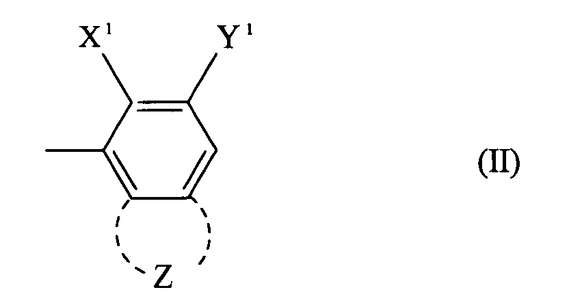 wherein R4 represents a hydrogen atom, a substituted or non-substituted alkyl group, and a substituted or non-substituted aryl group;
 wherein R5 represents a hydrogen atom, a substituted or non-substituted alkyl group, and a substituted or non-substituted aryl group;
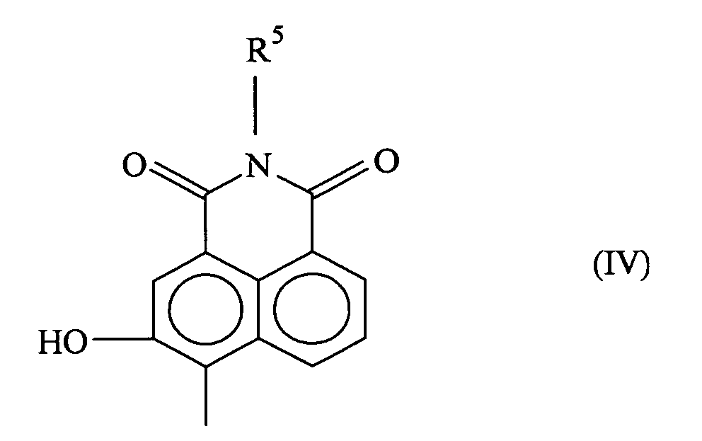 wherein Y represents a divalent aromatic hydrocarbon group or wherein Y together with the N-atoms it is bonded to forms a heterocyclic group;
 wherein Y represents a divalent aromatic hydrocarbon or wherein Y together with the N-atoms it is bonded to forms a heterocyclic group;
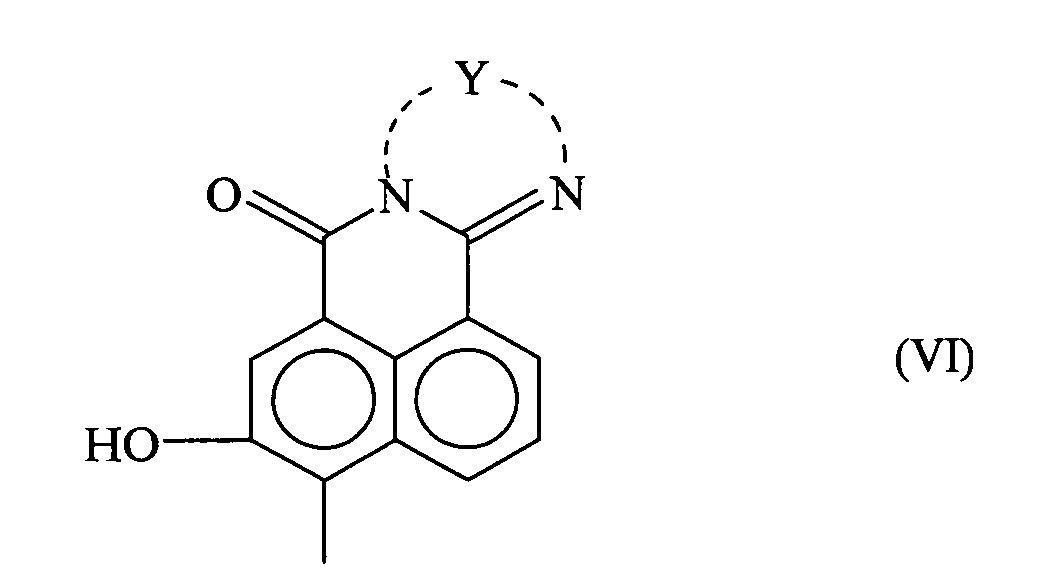 wherein R10 represents a hydrogen atom, an alkyl group, a carboxyl group, and a carboxyester group and Ar1 is a substituted or non-substituted aromatic hydrocarbon group; and
 wherein R11 represents a hydrogen atom, an alkyl group, a carboxyl group, and a carboxyester and Ar2 is a substituted or non-substituted aromatic hydrocarbon group.
- It is still further preferred that, the electrophotographic photoreceptor (1; 11; 21; 31; 51; 71) mentioned above, the
charge generation layer 102 contains a disazo pigment represented by the following formula (1)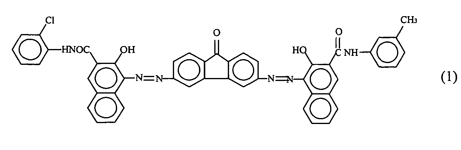
- It is still further preferred that, in the electrophotographic photoreceptor (1; 11; 21; 31; 51; 71) mentioned above, the
charge generation layer 102 has a reflectivity of from 17 to 19 %. - As another aspect of the present invention, an electrophotographic apparatus (100; 200; 300; 400; 500; 600) is provided which contains the electrophotographic photoreceptor (1; 11; 21; 31; 51; 71) mentioned above, a charger (2; 12; 22; 32; 52; 72) configured to uniformly charge the surface of the photoreceptor (1; 11; 21; 31; 51; 71), an image irradiator (3; 13; 23; 33; 53; 73) configured to irradiate the uniformly charged electrophotographic photoreceptor (1; 11; 21; 31; 51; 71) with light to form a latent electrostatic image thereon, a developing device (4; 14; 24; 34; 54; 74) configured to develop the latent electrostatic image with a
toner 5, a transfer device (6, 16; 26; 36; 46; 56; 76) configured to transfer the developed image to a receiving material (8; 28; 38; 58; 78) and a cleaner (7; 17; 27; 37; 57; 77) configured to remove any toner remaining on the photoreceptor (1; 11; 21; 31; 51; 71). In the electrophotographic apparatus, the electrophotographic photoreceptor (1; 11; 21; 31; 51; 71) further satisfies the following relationship: 12 (V/µm) ≤ electric field intensity (V/D) ≤ 35 (V/µm), wherein D (µm) represents a thickness of thecharge transport layer 103 of the electrophotographic photoreceptor (1; 11; 21; 31; 51; 71) and V (V) represents an absolute potential of the surface of the electrophotographic photoreceptor (1; 11; 21; 31; 51; 71) due to charging. - Alternatively the electrophotographic apparatus contains an electrophotograpnic photoreceptor (1; 11; 21; 31; 51; 71) having a
charge generation layer 102 including the disazo pigment (I) and having a light transmittance of from 35 to 65 % against light to form a latent electrostatic image on the electrophotographic photoreceptor (1; 11; 21; 31; 51; 71) . - It is preferred that, in the electrophotographic apparatus (100; 200; 300; 400; 500; 600) mentioned above, the electrophotographic photoreceptor (1; 11; 21; 31; 51; 71) satisfies the following relationship: 15 (V/µm) ≤ electric field intensity (V/D) ≤ 32 (V/µm).
- It is still further preferred that electrophotographic apparatus (100; 200; 300; 400; 500; 600) mentioned above, the
toner 5 for use in developing the latent electrostatic image has a sphere form. - It is still further preferred that the electrophotographic apparatus (100; 200; 300; 400; 500; 600) mentioned above further contains an intermediate transfer device (40; 80) to which multiple separate color toner images developed on the electrophotographic photoreceptor (1; 11; 21; 31; 51; 71) with separate color toners are transferred in a first step to form an overlaid color toner image on the intermediary transfer device (40; 80) while overlaying the separate color images thereon and from which the overlaid color toner image is transferred in a second step to the receiving material (8; 28; 38; 58; 78).
- It is still further preferred that, in the alternative electrophotographic apparatus (100; 200; 300; 400; 500; 600), the
charge generation layer 102 includes a disazo pigment represented by the following formula (1).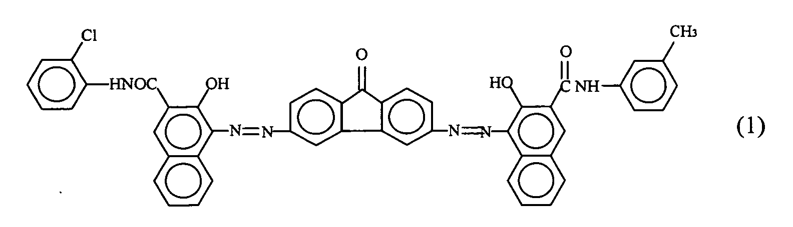
- As another aspect of the present invention, a process cartridge 300 is provided which includes the electrophotographic photoreceptor (1; 11; 21; 31; 51; 71) mentioned above, optionally an image irradiator (3; 13; 23; 33; 53; 73) configured to irradiate the uniformly charged electrophotographic photoreceptor (1; 11; 21; 31; 51; 71) with light to form a latent electrostatic image thereon, and at least one of preferably all of the following devices: a charger (2; 12; 22; 32; 52; 72) configured to uniformly charge a surface of the electrophotographic photoreceptor (1; 11; 21; 31; 51; 71); a developing device (4; 14; 24; 34; 54; 74) configured to develop the latent electrostatic image with a toner 5; a transfer device (6, 16; 26; 36; 46; 56; 76) configured to transfer the developed image to a receiving material(8; 28; 38; 58; 78); a cleaner (7; 17; 27; 37; 57; 77) configured to remove any toner remaining on the electrophotographic photoreceptor (1; 11; 21; 31; 51; 71) ; and a quencher 30 configured to discharge the surface of the electrophotographic photoreceptor (1; 11; 21; 31; 51; 71) .
- As another aspect of the present invention, a method of manufacturing the photoreceptor (1; 11; 21; 31; 51; 71) mentioned above is provided which includes the steps of forming the
conductive substrate 101, theundercoat layer 104 located overlying theconductive substrate 101, forming acharge generation layer 102 located overlying theundercoat layer 104 and acharge transport layer 103 located overlying thecharge generation layer 102. - These and other objects, features and advantages of the present invention will become apparent upon consideration of the following description of the preferred embodiments of the present invention taken in conjunction with the accompanying drawings.
- Various other objects, features and achieved advantages of the present invention will be more fully appreciated as the same becomes better understood from the detailed description when considered in connection with the accompanying drawings in which like reference numerals designate corresponding parts throughout and wherein:
- FIGS. 1 to 6 are schematic views illustrating embodiments of the electrophotographic apparatus of the present invention;
- FIGS. 7 and 8 are schematic view illustrating the cross sections of embodiments of the photoreceptor of the present invention;
- FIGS. 9 to 11 are schematic views for explaining the residual image problem; and
- FIGS. 12A to 12C are schematic views for explaining the change of the potential of a photoreceptor during the image forming processes.
-
- The inventors of the present invention have discovered that an electrophotographic apparatus producing a high density image with a high speed often causes the residual image problem but occurrence of the residual images can be effectively restrained by using an electrophotgraphic photoreceptor having a specific reflectivity or a specific light transmittance in the irradiation light wavelength band of the photoreceptor and a specific range electric field intensity (V/D), wherein D (µm) is a thickness of the
CTL 102 of the photoreceptor and V(V) is an absolute voltage of the surface of the photoreceptor due to charging, and further made of a disazo pigment having a specific structure. - In general, an electrophotographic photoreceptor having a multi-layer structure has side effects such as deterioration in sensitivity and voltage rise at an exposed portion when the reflectivity of the
CGL 102 against light having the highest reflectivity therefor is raised or when the light transmittance of theCGL 102 against light having a wavelength of the image irradiation light source is lowered, namely the thickness of theCGL 102 is thin. The reason why the wavelength having the highest reflectivity is used is that it is easy to determine and control. However, the inventors of the present invention have discovered that a disazo pigment can effectively restrain these side effects. - Azo pigments are generally prepared by reacting an aromatic diazonium salt and a coupling component (coupler) in the presence of a salt. Among various kinds of combinations, azo pigments having at least two azo groups such as disazo pigments or trisazo pigments are typically used as CGM. The structure of these azo pigments greatly affects electrostatic characteristics such as sensitivity.
- For these azo pigments, naphthol based couplers are greatly preferred in terms of sensitivity. However, the sensitivity varies depending on the state of particles of an azo pigment used as CGM for an electrophotographic photoreceptor.
- The disazo pigments represented by the formula (I) for use in the present invention (i.e., the disazo pigments having a coupler remaining group represented by the following formulae (II) to (VIII)) have a stable intermolecular associate forming state due to the hydrogen bonding of the coupler remaining group. In addition, the particle state of the disazo pigments achieved when a layer of the disazo pigments is formed on an electrophotographic photoreceptor is extremely stable. Due to these factors, a photoreceptor made of these disazo pigments has excellent initial sensitivity, excellent maintainabiliy and excellent light resistance. As a result, the side effects such as deterioration in sensitivity and voltage rise at an exposed portion can be restrained by improving the reflectivity against light having the highest reflectivity or the light transmittance in the irradiation light wavelength band of the photoreceptor.wherein, A and B represent coupler remaining groups represented by the following formulae (II) to (VIII);
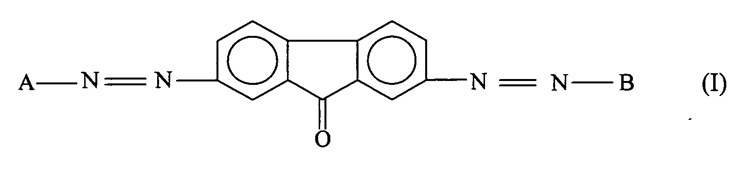 wherein, X1 represents -OH, -NHCOCH3, and -NHSO2CH3, Y1 represents -CON(R2)(R3), -CONHN = C(R6)(R7), -CONHN(R8)(R9),-CONHCONH(R12), a hydrogen atom, COOH, -COOCH3, COOC6H5 and a benzimidazol group, wherein R2 and R3 independently represent a hydrogen atom, a substituted or non-substituted alkyl group, a substituted or non-substituted aryl group and a substituted or non-substituted heterocyclic group or wherein R2 and R3 when taken together can form a ring with the nitrogen atom they are bonded to, R6 and R7 independently represent a hydrogen atom, a substituted or non-substituted alkyl group, a substituted or non-substituted aralkyl group, a substituted or non-substituted aryl group, a substituted or non-substituted styryl group and a substituted or non-substituted heterocyclic group or wherein R6 and R7 when taken together can form a ring with the nitrogen atom they are bonded to, R8 and R9 independently represent a hydrogen atom, a substituted or non-substituted alkyl group, a substituted or non-substituted aralkyl group, a substituted or non-substituted aryl group, a substituted or non-substituted styryl group and a substituted or non-substituted heterocyclic group or wherein R8 and R9 when taken together with the carbon atom they are bonded to can form a five-membered ring or six-membered ring optionally having a condensed aromatic ring, and R12 represents a substituted or non-substituted alkyl group, a substituted or non-substituted aryl group and a substituted or non-substituted heterocyclic group, and Z represents a remaining group which is fused with the benzene ring to form a polycyclic aromatic structure or a heterocyclic structure selected from the group consisting of a naphthalene ring, an anthracene ring, a carbazole ring, a benzocarbazole ring, a dibenzocarbazole ring, a dibenzofuran ring, a benzonaphthofuran ring and a dibenzothiophene ring, each of which can have at least one substituent;
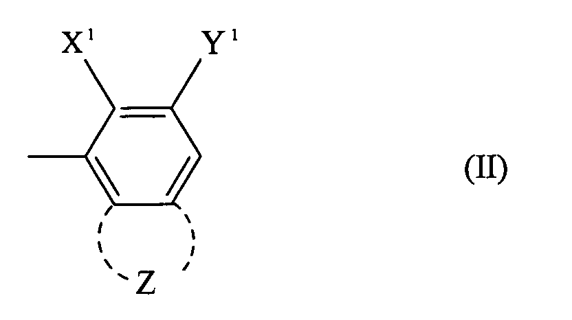 wherein R4 represents a hydrogen atom, a substituted or non-substituted alkyl group, and a substituted or non-substituted aryl group;
 wherein R5 represents a hydrogen atom, a substituted or non-substituted alkyl group, and a substituted or non-substituted aryl group;
 wherein Y represents a divalent aromatic hydrocarbon group or wherein Y together with the N-atoms it is bonded to forms a heterocyclic group;
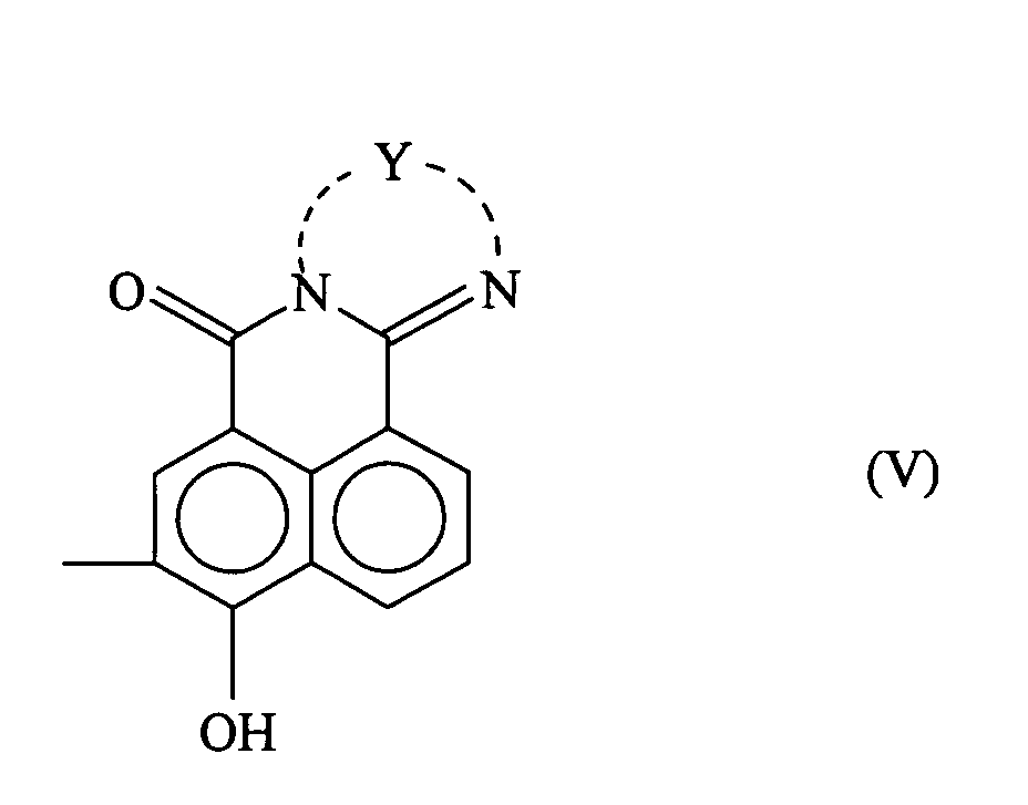 wherein Y represents a divalent aromatic hydrocarbon or wherein Y together with the N-atoms it is bonded to forms a heterocyclic group;
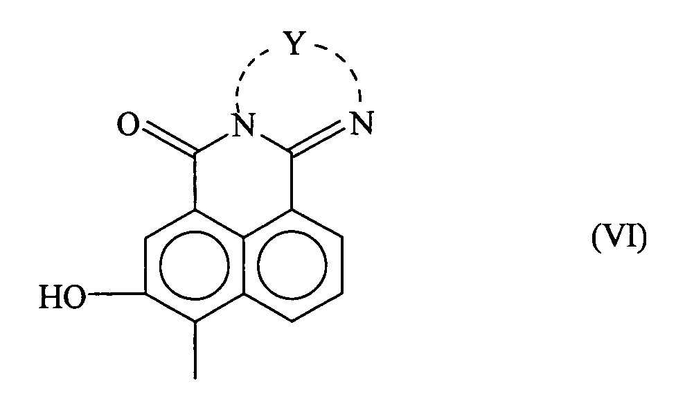 wherein R10 represents a hydrogen atom, an alkyl group, a carboxyl group, and a carboxyester group and Ar1 is a substituted or non-substituted aromatic hydrocarbon group; and
 wherein R11 represents a hydrogen atom, an alkyl group, a carboxyl group, and a carboxyester and Ar2 is a substituted or non-substituted aromatic hydrocarbon group.
- The bond in formulae (II) between coupler and azo group can be in any position to X1 or Y1, but is preferably in ortro position to X1.
- The substituted or non-substituter alkyl group preferably is an alkyl group comprising 1 to 20 carbon atoms, more preferably 1 to 10 carbon atoms, and most preferably 1 to 4 carbon atoms. Suitable examples are methyl, ethyl, propyl, butyl, pentyl, vinyl, allyl, cyclohexyl, cycloheptyl, 2-ethyl hexyl amongst others.
- The substituted or non-substituter aryl group preferably is an aryl group comprising 6 to 18 carbon atoms, more preferably 6 to 14 carbon atoms, and most preferably 6 to 10 carbon atoms. Suitable examples are benzene, naphthalene, anthracene, phenantrene, fluorine (fluorene) and the like.
- The substituted or non-substituter aralkyl group preferably comprises 6 to 18 carbon atoms in the aryl group and 1 to 10 carbon atoms in the alkylene group, more preferably 6 to 10 carbon atoms in the aryl group and 1 to 4 carbon atoms in the alkylene group. Suitable examples are phenylmethyl and diphenyl methyl.
- The substituted or non-substituted heterocyclic group preferably comprises from 2 to 20 carbon atoms, more preferably 2 to 10 carbon atoms, and 1 to 3, preferably 1 hetero atom(s) selected from the group, consisting of nitrogen, sulfur and oxygen. Preferably the hetero atom(s) is/are nitrogen or oxygen. Suitable examples are furane, thiophene, pyrroline, oxazole, thiazole, pyrazole, isooxazole, imidazole, benzofurane, indole, benzoxazole, benzothiazole, benzimidazole, carbazole, morpholine, pyridine, chinoline, acridine, pyrimidine, pyrazine, pyrane, α-chromene, and xanthene.
- The substituted or non-substituted aromatic hydrogarbon groups Ar1 and Ar2, preferably have about 6 to 30 carbon atoms, preferably 6 to 14 carbon atoms and most preferably 6 to 10 carbon atoms. It can be any of the groups listed above for the aryl and aralkyl groups. Preferably Ar1 or Ar2 are phenyl or phenylmethyl.
- Each of the above alkyl, alalkyl, aryl, aromatic hydrocarbon and heterocyclic groups may have one or more substituents. These are preferably selected from the group consisting of -OH, -SH, =O, -NR13R14, wherein R13 and R14 independently are H or C1-4 alkyl, C6-10 aryl, C1-4 alkoky, C1-4 alkylthio, C6-10 aryloxy, halogene (CL, F, Br, I), carboxy, carboxyl C1-4 ester, nitro, sulfinyl and sulfonyl. Preferably the substituent is one or more of methyl, ethyl, methoxy, dimethylamino, -OH, -Cl, -F =O and carboxy.
- That is, to restrain the occurrence of residual images, by using a disazo pigment having a specific structure for a photoreceptor having a photosensitive layer having a specific reflectivity against light having a wavelength having the highest reflectivity or a specific light transmittance in the irradiation light wavelength band and having a specific range electric field intensity (V/D), an electrophotographic apparatus capable of producing quality images at a high speed can be obtained. With regard to the reflectivity, by specifying a reflectivity of a
CGL 102 measured by a spectrophotometric colorimeter in a range of from 360 nm to 740 nm after anundercoat layer 104 and theCGL 102 are formed, a stable value is obtained regardless of the specification such as kind and thickness of aCTL 102 overlaid on theCGL 102. In addition, before theCTL 102 serving as outermost layer is coated, the amount of theCGL 102 attached can be determined and thus coating conditions for theCGL 102 can be controlled by feedback in the coating processes. - When the reflectivity against light having a wavelength showing the highest reflectivity at the
CGL 102 is too low or when the light transmittance of theCGL 102 in the irradiation light wavelength band is too low (i.e., the thickness of theCGL 102 is thick enough to lower the light transmittance), characteristics such as optical decay, namely, photosensitivity, are excellent in most cases but charging stability tends to be bad and deteriorates for repeated uses in a dark place. In addition, such a photoreceptor tends to be vulnerable to the reversed bias at a transfer portion. Thereby when the photoreceptor is recharged, a potential difference occurs between the portion which is irradiated by an irradiator and the portion which is not. Consequently, a residual image is obtained at a half tone portion having a dense writing. - Therefore, a photoreceptor having a high reflectivity against light having the highest reflectivity at the CGL is good or a photoreceptor having a thin CGL 102 (i.e., the light emittance in the irradiation light wavelength band is high) is good. However, when the reflectivity or the light transmittance is too high, optical decay characteristics deteriorate and a potential at an exposed portion rises. Further, when the reflectivity or the light transmittance is high and the photoreceptor is repetitively used while the electric field intensity is high, electrostatic stresses on the photosensitive layer increase, resulting in accumulation of light fatigue. Thus residual images tend to occur in this case. It is important to control the electric field intensity within a low range.
- However, when the electric field intensity is low, the electrostatic contrast obtained tends to be insufficient. Therefore, it is important that the potential at an electrophotographic photoreceptor after optical decay after irradiation sufficiently drops. However, when no suitable material is used, , optical response of the photoreceptor is good but electrostatic contrast becomes insufficient, which causes a problem in image formation. As a result of the intensive study on various kinds of compounds, it has been found that the disazo pigments represented by the following formula (I) satisfies the characteristics mentioned above.
- Thus the present invention was made. In addition, a process cartridge and an electrophotographic apparatus producing full-color images using this electrophotographic mechanism capable of producing quality image without having a residual image.
- The electrophotographic photoreceptor for use in the present invention is described in detail with reference to the accompanying drawings.
- First, the electrophotographic apparatus is described with reference to the accompanying drawings.
- Fig. 1 is a schematic diagram illustrating an embodiment of the electrophotographic apparatus of the present invention and variations thereof described later are also within the scope of the present invention.
- In Fig. 1, a photoreceptor 1 is an electrophotographic photoreceptor satisfying the requirements of the present invention.
- The photoreceptor 1 has a drum form, but photoreceptors having a form such as sheet-form and endless belt-form can also be used.
- Around the photoreceptor 1, a discharging
lamp 10 to decrease charges remaining on the photoreceptor 1, acharger 2 configured to charge the photoreceptor 1, animagewise light irradiator 3 configured to irradiate the photoreceptor 1 with imagewise light to form an electrostatic latent image on the photoreceptor 1, an image developing device 4 configured to develop the latent image with atoner 5 to form a toner image on the photoreceptor 1, and acleaner 7 including a cleaning blade configured to clean the surface of the photoreceptor 1 are arranged in contact with or in close piximity to the photoreceptor 1. The toner image formed on the photoreceptor 1 is transferred on a receiving material 8 (e.g., receiving paper) by atransfer device 6. The toner image on the receivingmaterial 8 is fixed thereon by afixer 9. - As the
charger 2, any known chargers such as corotrons, scorotrons, solid state chargers, and roller chargers can be used. Among the chargers, contact chargers and short-range chargers are preferably used in terms of power consumption. Particularly, short-range chargers which can charge a photoreceptor while a proper gap is formed between the chargers and the surface of the photoreceptor are more preferably used. - As the
transfer device 6, the above-mentioned known chargers can be used. Among the chargers, a combination of a transfer charger and a separating charger is preferably used. - Suitable light sources for use in the imagewise
light irradiator 3 and the discharginglamp 10 include fluorescent lamps, tungsten lamps, halogen lamps, mercury lamps, sodium lamps, light emitting diodes (LEDs), laser diodes (LDs), light sources using electroluminescence (EL), and the like. In addition, in order to obtain light having a desired wavelength range, filters such as sharp-cut filters, band pass filters, near-infrared cutting filters, dichroic filters, interference filters, color temperature converting filters and the like can be used. - When the toner image formed on the photoreceptor 1 by the image developing device 4 is transferred onto the receiving
paper 8, not all of the toner images is transferred on the receivingpaper 8, and toner particles remain on the surface of the photoreceptor 1. The residual toner is removed from the photoreceptor 1 by thecleaner 7. Suitable cleaners for use as thecleaner 7 include cleaning blades made of a rubber, fur brushes and mag-fur brushes. - When the photoreceptor 1 which is previously charged positively (or negatively) is exposed to imagewise light, an electrostatic latent image having a positive (or negative) charge is formed on the photoreceptor 1. When the latent image having a positive (or negative) charge is developed with a toner having a negative (or positive) charge, a positive image can be obtained. In contrast, when the latent image having a positive (negative) charge is developed with a toner having a positive (negative) charge, a negative image (i.e., a reversed image) can be obtained. As the developing method, known developing methods can be used. In addition, as the discharging methods, known discharging methods can also be used.
- Fig. 2 is a schematic view illustrating another embodiment of electrophotographic process of the present invention. The photoreceptor 1 is an electrophotographic photoreceptor satisfying the requirements of the present invention and has a belt form. The belt-
form photoreceptor 11 is rotated by rollers R1 and R2. Thephotoreceptor 11 is charged with acharger 12, and then exposed to imagewise light emitted by an imagewise light irradiator 13 to form an electrostatic latent image on thephotoreceptor 11. The latent image is developed with animage developing device 14 to form a toner image on thephotoreceptor 11. The toner image is transferred onto a receiving paper (not shown) using atransfer device 16. After the toner image transferring process, the surface of thephotoreceptor 11 is cleaned with a cleaningbrush 17 after performing a pre-cleaning light irradiating operation using apre-cleaning light irradiator 18. Then thephotoreceptor 11 is exposed to light emitted by a discharginglight source 19 to reduce the charge remaining thereon. In the pre-cleaning light irradiating process, light irradiates thephotoreceptor 11 from the side of thesubstrate 101 thereof. In this case, thesubstrate 101 has to be light-transmissive. - The elecctrophotographic processes for use in the present invention is not limited to the processes shown in FIGS. 1 and 2. For example, in Fig. 2, the pre-cleaning light irradiating operation can be performed from the photosensitive layer side of the
photoreceptor 11. In addition, the light irradiation in the imagewise light irradiating process and the discharging process may be performed from thesubstrate 101 side of thephotoreceptor 11. - Further, a pre-transfer light irradiation operation, which is performed before transferring the toner image, and a preliminary light irradiation operation, which is performed before the imagewise light irradiation, and other light irradiation operations may also be performed.
- The above-mentioned image forming unit may be fixedly set in an electrophotographic apparatus such as copiers, facsimile machines and printers. However, the image forming unit can be set therein as a process cartridge. The process cartridge means an image forming unit which includes a photoreceptor and at least one or more or all of a charger, an imagewise light irradiator, an image developing device, a transfer device, a cleaner, and a queencher.
- Various types of process cartridges can be used in the present invention. An embodiment of the process cartridge of the present invention is illustrated in FIG. 3.
- In Fig. 3, the process cartridge includes a photoreceptor 21, which is the photoreceptor of the present invention, a
charger 22 configured to charge the photoreceptor 21, an image developing device (a developing roller) 24 configured to develop an electrostatic latent image, which is formed on the photoreceptor by animagewise light irradiator 23, with a toner to form a toner image, atransfer device 26 configured to transfer the toner image to a receivingmaterial 28, and acleaning blade 27 configured to clean the surface of the photoreceptor 21.Numerals - FIG. 4 illustrates another embodiment of the electrophotographic apparatus of the present invention. With reference to FIG. 4, the electrophotographic apparatus has a
photoreceptor 31 which is the photoreceptor of the present invention. Around thephotoreceptor 31, acharger 32, animagewise light irradiator 33, animage developing unit 34 having a black image developing device 34Bk, a cyanimage developing device 34C, a magentaimage developing device 34M and a yellowimage developing device 34Y, anintermediate transfer belt 40 serving as an intermediate transfer medium, and a cleaner 37 are arranged. - The image developing devices 34Bk, 34C, 34M and 34Y can be independently controlled, and each of the image developing devices is independently driven when desired. Toner images formed on the
photoreceptor 31 are transferred onto theintermediate transfer belt 40 by afirst transfer device 36. Theintermediate transfer belt 40 is brought into contact with thephotoreceptor 31 by thefirst transfer device 36 only when a toner image on thephotoreceptor 31 is transferred thereto. The toner images overlaid on theintermediate transfer belt 40 are transferred onto a receivingmaterial 38 by asecond transfer device 46, and the toner images are fixed on the receivingmaterial 38 by afixer 39. Thesecond transfer device 46 is brought into contact with theintermediate transfer belt 40 only when the transfer operation is performed. - In an electrophotographic apparatus having a drum-form transfer device, color toner images are transferred onto a receiving material electrostatically attached to the transfer drum. Therefore, an image cannot be formed on a thick paper. However, in the electrophotographic apparatus as illustrated in FIG. 4, each toner image is formed on the intermediate transfer belt and the overlaid toner images are transferred onto a receiving material. Therefore, an image can be formed on any kinds of receiving materials. The image forming method using an intermediate transfer medium can be applied to the electrophotographic apparatus as illustrated in FIGS. 1-3, and 5 as well as the electrophotographic apparatus illustrated in FIGS. 4 and 6.
- FIG. 5 illustrates another embodiment of the electrophotographic apparatus of the present invention.
- The electrophotographic apparatus has four color image forming sections, i.e., yellow, magenta, cyan and black image forming sections. The image forming sections include
respective photoreceptors - Around each of the photoreceptors (51Y, 51M, 51C or 51Bk), a charger (52Y, 52M, 52C or 52Bk), an imagewise light irradiator (53Y, 53M, 53C or 53Bk), an image developing device (54Y, 54M, 54C or 54Bk), and a cleaner (57Y, 57M, 57C or 57Bk) are arranged. In addition, a feed/
transfer belt 60, which is arranged below the image forming sections, is tightly stretched by rollers R3 and R4. The feed/transfer belt 60 is attached to or detached from the photoreceptors 51 bytransfer devices material 58. The resultant color toner image is fixed by afixer 59. - The tandem-type electrophotographic apparatus illustrated in FIG. 5 has a plurality of photoreceptors 51 for forming four color images, and color toner images which can be formed in parallel can be transferred onto the receiving
material 58. Therefore, the electrophotographic apparatus can form full color images at a much higher speed than that of such an electrophotographic apparatus as illustrated in FIG. 4. - FIG. 6 illustrates another embodiment of the electrophotographic apparatus of the present invention, which is a tandem-type color electrophotographic apparatus having an intermediate transfer medium.
- The electrophotographic apparatus has four color image forming sections, i.e., yellow, magenta, cyan and black image forming sections. The image forming sections include
respective photoreceptors - Around each of the photoreceptors (71Y, 71M, 71C or 71Bk), a charger (72Y, 72M, 72C or 72Bk), an imagewise light irradiator (73Y, 73M, 73C or 73Bk), an image developing device (74Y, 74M, 74C or 74Bk), and a cleaner (77Y, 77M, 77C or 77Bk) are arranged. In addition, an
intermediate transfer belt 80, which is arranged below the image forming sections, is tightly stretched by rollers R5 and R6 and other rollers. Theintermediate transfer belt 80 is attached to or detached from the photoreceptors bytransfer devices intermediate transfer belt 80 are transferred onto a receivingmaterial 78 at once by atransfer device 86. Then the color toner images are fixed by afixer 79. - Next, the organic photoreceptor of the present invention will be explained in detail referring to drawings.
- FIG. 7 illustrates a schematic cross section of an embodiment of the photoreceptor having the layer structure of the present invention. The photoreceptor has an
electroconductive substrate 101 , a charge generation layer 102 (CGL 102) 102 and a charge transport layer 103 (CTL 102) 103. - FIG. 8 illustrates a schematic cross section of another embodiment of the photoreceptor having the layer structure of the present invention. The photoreceptor has a structure such that an
undercoat layer 104 is formed between thesubstrate 101 and theCGL 102 of FIG. 7. - Suitable materials for use as the
electroconductive substrate 101 include materials having a volume resistance not greater than 1010 Ω · cm. Specific examples of such materials include plastic or paper cylinders or films, on the surface of which a metal such as aluminum, nickel, chromium, nichrome, copper, gold, silver, platinum, iron and the like, or a metal oxide such as tin oxides, indium oxides and the like, is formed by a method such as vapor deposition and sputtering. In addition, a plate of a metal such as aluminum, aluminum alloys, nickel and stainless steel can be used. A metal cylinder can also be used as thesubstrate 101, which is prepared by tubing a metal such as aluminum, aluminum alloys, nickel and stainless steel by a method such as drawing, impact molding, extrusion molding, extrusion drawing or cutting, and then subjecting the surface of the tube to cutting, super finishing, polishing and the like treatments. - The photosensitive layer of the present invention is a multi-layered photosensitive layer having the
CGL 102 on theelectroconductive substrate 101 and theCTL 102 103 over laid on theCGL 102. The structures of each layer of this multi-layered photosensitive layer are now described. - The
CGL 102 includes a CGM as a main component, and optionally includes a binder resin. As CGMs for use in the present invention, considering the characteristics mentioned above, at least one of the main components is a disazo pigment represented by formula (I) described before. Specific examples of such disazo pigments include a compound having a benzene ring substituent having Cl at the ortho position at each end of the compound such as (2,7-bis[3-(2-chlorophenyl)carbamoyl-2-hydroxy-1-naphthylazo]-9-fluorenone. Specific suitably preferred examples among the compounds represented by formula (I) is a disazo pigment having the structure represented by the following formula (1).
- These CGMs can be used alone or in combination.
- Suitable binder resins, which are optionally included in the
CGL 102, include polyamide, polyurethane, epoxy resins, polyketone, polycarbonate, polyarylate, silicone resins, acrylic resins, polyvinyl butyral, polyvinyl formal, polyvinyl ketone, polystyrene, poly-N-vinylcarbazole, polyacrylamide, and the like resins. - These resins can be used alone or in combination.
- In addition, charge transport polymers can be used as the binder resin of the
CGL 102. Further, low molecular weight CTMs can be added to theCGL 102 if desired. - The CTMs are classified into positive-hole transport materials and electron transport materials and further classified into low molecular weight CTMs and charge transport polymers.
- Specific examples of the electron transport materials include electron accepting materials such as chloranil, bromanil, tetracyanoethylene, tetracyanoquinodimethane, 2,4,7-trinitro-9-fluorenon, 2,4,5,7-tetranitro-9-fluorenon, 2,4,5,7-tetanitroxanthone, 2,4,8-trinitrothioxanthone, 2,6,8-trinitro-4H-indeno[1,2-b]thiophene-4-one, 1,3,7-trinitrodibenzothiophene-5,5-dioxide, and the like.
- These electron transport materials can be used alone or in combination.
- Specific examples of the positive-hole transport materials include oxazole derivatives, oxadiazole derivatives, imidazole derivatives, triphenyl amine derivatives, 9-(p-diethylaminostyrylanthracene), 1,1-bis-(4-dibenzylaminophenyl)propane, styryl anthracene, styryl pyrazoline, phenyl hydrazone, α-phenyl stilbene derivatives, thiazole derivatives, triazole derivatives, phenazine derivatives, acridine derivatives, benzofuran derivatives, benzimidazole derivatives, thiophene derivatives, etc.
- The positive-hole transport materials can be used alone or in combination.
- Suitably preferred methods for forming the
CGL 102 include casting methods from a solution dispersion system. - The casting methods for forming the
CGL 102 typically include the following steps: - (1) preparing a coating liquid by mixing the CGMs mentioned above
with a solvent such as tetrahydrofuran, cyclohexanone, dioxane,
dichloroethane, butanone and the like, optionally together with
a binder resin and an additive, and then dispersing the materials
with a ball mill, an attritor, a sand mill or the like, to prepare
a
CGL 102 coating liquid; - (2) coating the
CGL 102 coating liquid, which is diluted if necessary, on asubstrate 101 by a method such as dip coating, spray coating and bead coating; and - (3) drying the coated liquid to form a
CGL 102. -
- The thickness of the
CGL 102 formed as mentioned above satisfies the following conditions: the reflectivity of theCGL 102 against light having a wavelength showing the highest reflectivity therefor when measured by a spectrophotometric colorimeter in the range of from 360 nm to 740nm after anundercoat layer 104 and theCGL 102 are formed is from 15 to 21 % and preferably from 17 to 19 %; and/or light transmittance of theCGL 102 against light having a wavelength used in the image irradiation is from 35 to 65 % and preferably from 40 to 55 %. When the light transmittance is too low (i.e., theCGL 102 is formed thick enough to reduce the light transmittance), characteristics such as optical decay, namely, photosensitivity, are excellent in most cases but charging stability tends to be bad and therefore deteriorates for repeated uses in a dark place. In addition, such a photoreceptor tends to be vulnerable to reversed bias at a transfer portion. Thereby when the photoreceptor is recharged, a potential difference occurs between the portion which is irradiated by an irradiator and the portion which is not. Consequently, a residual image is obtained at a half tone portion having a dense writing. - Therefore, it is good to reduce the amount of the
CGL 102 attached, namely, to have anundercoat layer 104 and aCGL 102 having a high reflectivity against light having a wavelength showing the highest reflectivity at theCGL 102 and/or to have a thin CGL 102 (i.e., the light transmittance in the wavelength band of the irradiation light is high). However, when the reflectivity and/or light transmittance is too high, optical decay characteristics deteriorate and a potential at an exposed portion rises. - Next, the
CTL 102 103 is now described. - The
CTL 102 103 is typically prepared by preparing aCTL 102 coating liquid in which a mixture of a CTM and a binder resin or a charge transport polymer material is dissolved or dispersed in a solvent, and then coating the coating liquid followed by drying. - Specific examples of the polymers for use as the binder resin of the
CTL 102 include thermoplastic resins and thermosetting resins such as polystyrene, styrene / acrylonitrile copolymers, styrene / butadiene copolymers, styrene / maleic anhydride copolymers, polyester, polyvinyl chloride, vinyl chloride / vinyl acetate copolymers, polyvinyl acetate, polyvinylidene chloride, polyarylate, polycarbonate, cellulose acetate resins, ethyl cellulose resins, polyvinyl butyral, polyvinyl formal, polyvinyl toluene, acrylic resins, silicone resins, fluorine-containing resins, epoxy resins, melamine resins, urethane resins, phenolic resins and alkyd resins, but are not limited thereto. - These polymer materials can be used alone or in combination. In addition, copolymers of the monomers of the polymer materials mentioned above can also be used. Further, copolymers of the monomers with a CTM can also be used.
- When an electrically inactive polymer is used in order to impart good stability to withstand environmental conditions to the resultant photoreceptor, resins such as polyester, polycarbonate, acrylic resins, polystyrene, polyvinylidene chloride, polyethylene, polypropylene, fluorine-containing resins, polyacrylonitrile, acrylonitrile / styrene / butadiene copolymers, acrylonitrile / styrene copolymers and ethylene / vinyl acetate copolymers are preferably used. Electrically inactive charge transport polymer materials mean polymers which do not have a structure having a photoconductive property, such as the triarylamine structure.
- When these resins are used as an additive together with a binder resin, the content thereof is preferably not greater than 50 % by weight of the sum of additive and binder in view of photosensitivity of the resultant photoreceptor.
- Specific examples of the CTMs for use in the
CTL 102 include the low molecular weight electron transport materials, low molecular weight positive hole transport materials, and charge transport polymer materials mentioned above. - When a low molecular weight CTM is used, the content thereof is from 40 to 200 parts by weight, and preferably from 70 to 150 parts by weight, per 100 parts by weight of the resin components included therein. When a charge transport polymer is used, the content thereof is from 0 to 500 parts by weight, and preferably from 0 to 150 parts by weight, per 100 parts by weight of the charge transport components included therein.
- When two or more kinds of CTMs are included in the
CTL 102, the difference in ionization potential between the two or more kinds of CTMs is as small as possible, specifically the difference is preferably not greater than 0.15 eV. In this case, it is prevented that one of the CTMs serves as a trap of the other CTMs. - In order to impart high photosensitivity to a photoreceptor, the content of the CTMs in the
CTL 102 is preferably not less than 70 parts by weight per 100 parts by weight of the resin components in theCTL 102. - Suitable solvents for use in the
CTL 102 coating liquid include ketone such as methyl ethyl ketone, acetone, methyl isobutyl ketone, and cyclohexanone; ethers such as dioxane, tetrahydrofuran, and ethyl cellosolve; aromatic solvents such as toluene, and xylene; halogen-containing solvents such as chlorobenzene, and dichloromethane; esters such as ethyl acetate and butyl acetate; etc. These solvents can be used alone or in combination. - The
CTL 102 can include one or more additives such as antioxidants, plasticizers, lubricants and ultraviolet absorbents, if desired. Specific examples thereof are mentioned below. These additives are added in theCTL 102 in an amount of from 0.1 to 50 parts by weight, preferably from 0.1 to 20 parts by weight, per 100 parts by weight of the resin components therein. The leveling agents are added in an amount of from 0.001 to 5 parts by weight per 100 parts by weight of the resin components therein. - Suitable coating methods for use in coating the
CTL 102 coating liquid include dip coating methods, spray coating methods, ring coating methods, roll coating methods, gravure coating methods, nozzle coating methods, screen coating methods, etc. Among them, the spray coating methods are preferred since agglomeration of fillers can be easily prevented. - The thickness of the
CTL 102 is generally from 15 to 40 µm, and preferably from 15 to 30 µm. When it is desired to form images having good resolution, the thickness of theCTL 102 is preferably not greater than 25 µm. It is also necessary to consider the electric field intensity of an electrophotographic apparatus. The electric field intensity is a value of V/D, wherein D (µm) represents a thickness of theCTL 102 of the photoreceptor and V (V) represents an absolute potential of the surface of the photoreceptor due to the charging. The electric field intensity is from 12 (V/µm) to 35 (V/µm) as mentioned above, and preferably from 15 to 32 (V/µm). - Further, when the electric field intensity is high, electrostatic stresses on the photosensitive layer increase, resulting in increase of light fatigue. Thus when the electric field intensity is low, electrostatic contrast obtained tends to be insufficient. Therefore, it is important to have a potential suitable for the thickness of the
CGL 102 used. - In the photoreceptor of the present invention, an
undercoat layer 104 can be formed between thesubstrate 101 and theCGL 102 to improve adhesion between thesubstrate 101 and the photosensitive layer; to prevent formation of moiré; to improve the coating property of the overlying layer; to reduce the residual potential; and to prevent injection of charges from thesubstrate 101 into the photosensitive layer. - The
undercoat layer 104 typically includes a resin as a main component. Since a photosensitive layer is typically formed on theundercoat layer 104 by coating a liquid including an organic solvent, the resin in theundercoat layer 104 preferably has good resistance to general organic solvents. - Specific examples of such resins include water-soluble resins such as polyvinyl alcohol resins, casein and polyacrylic acid sodium salts; alcohol soluble resins such as nylon copolymers and methoxymethylated nylon resins; and thermosetting resins capable of forming a three-dimensional network such as polyurethane resins, melamine resins, alkyd-melamine resins, epoxy resins and the like.
- The
undercoat layer 104 may include a fine powder of metal oxides such as titanium oxide, silica, alumina, zirconium oxide, tin oxide and indium oxide. - The
undercoat layer 104 can also be formed by coating a coating liquid using a proper solvent and a proper coating method mentioned above for use in the photosensitive layer. - In addition, metal oxide layers formed by a sol-gel method using a silane coupling agent, titanium coupling agent or a chromium coupling agent can also be used as the
undercoat layer 104. - Further, a layer of aluminum oxide which is formed by an anodic oxidation method and a layer of an organic compound such as polyparaxylylene or an inorganic compound such as SiO2, SnO2, TiO2, ITO or CeO2 which is formed by a vacuum evaporation method is also preferably used as the
undercoat layer 104. - The thickness of the
undercoat layer 104 is suitably from 0.1 to 10 µm and preferably from 1 to 5 µm. - In the photoreceptor of the present invention, one or more additives such as antioxidants, plasticizers, ultraviolet absorbents, low molecular weight charge transport materials and leveling agents can be used in one or more layers of the photosensitive layer, i.e.,
CGL 102,CTL 102, andundercoat layer 104, to improve the gas barrier property of the outermost layer of the photoreceptor and the stability thereof to withstand environmental conditions. - The following is typical materials for these compounds. (Antioxidant)
- Suitable antioxidants for use in the layers of the photoreceptor include the following compounds but are not limited thereto.
- 2,6-di-t-butyl-p-cresol, 2,4,6-tri-t-butylphenol, n-octadecyl-3-(4'-hydroxy-3',5'-di-t-butylphenol)propionate, styrenated phenol, 4-hydroxymethyl-2,6-di-t-butylphenol, 2,5-di-t-butylhydroquinone, cyclohexyl phenol, butylhydroxyanisole, 2,2'-methylene-bis-(4-ethyl-6-t-butylphenol), 4,4'-isopropylidenebisphenol, 1,1-bis(4-hydroxyphenyl)cyclohexane, 4,4'-methylene-bis (2,6-di-t-butylphenol), 2,6-bis(2'-hydroxy-3'-t-butyl-5'-methylbenzyl)-4-methylphenol, 1,1,3-tris-(2-methyl-4-hydroxy-5-t-butylphenyl)butane, 1,3,5-trismethyl-2,4,6-tris(3, 5-di-t-butyl-4-hydroxybenzyl)benzene, tetrakis-[methylene-3-(3' ,5' -di-t-butyl-4-hydroxyphenyl) propionate] methane, tris(3,5-di-t-butyl-4-hydroxyphenyl)isocyanate, tris[β -(3,5-di-t-butyl-4-hydroxyphenyl)propionyl-oxyethyl]isocyanat e, 4,4'-thiobis(4-methyl-6-t-butylphenol), 4,4'-thiobis (4-methyl-6-t-butylphenol,) etc.
- phenyl-α-naphthylamine, phenyl-β-naphthylamine, N,N' -diphenyl-p-phenylenediamine, N,N' -di-β-naphthyl-p-phenylenediamine, N-cyclohexyl-N'-phenyl-p-phenylenediamine, N-phenylene-N'-isopropyl-p-phenylenediamine, aldol-α-naphthylamine, 6-ethoxy-2,2,4-trimethyl-1,2-dihydroquinoline, etc.
- thiobis(β-naphthol), thiobis(N-phenyl-β-naphthylamine), 2-mercaptobenzothiazole, 2-mercaptobenzimidazole, dodecylmercaptan, tetramethylthirammonosulfide, tetramethylthiramdisulfide, nickeldibutylthiocarbamate, isopropylxanthate, dilaurylthiodipropionate, distearylthiodipropionate, etc.
- triphenyl phosphite, diphenyldecyl phosphite, phenyl isodecyl phosphite, tri(nonylphenyl)phosphite, 4, 4' -butylidene-bis (3-methyl-6-t-butylphenyl-ditridecylphosph ite), distearyl-pentaerythritol diphosphite, trilauryl trithiophosphite, etc.
- Suitable plasticizers for use in the layers of the photoreceptor include the following compounds but are not limited thereto:
- triphenyl phosphate, tricresyl phosphate, trioctyl phosphate, octyldiphenyl phosphate, trichloroethyl phosphate, cresyldiphenyl phosphate, tributyl phosphate, tri-2-ethylhexyl phosphate, triphenyl phosphate, and the like.
- dimethyl phthalate, diethyl phthalate, diisobutyl phthalate, dibutyl phthalate, diheptyl phthalate, di-2-ethylhexyl phthalate, diisooctyl phthalate, di-n-octyl phthalate, dinonyl phthalate, diisononyl phthalate, diisodecyl phthalate, diundecyl phthalate, ditridecyl phthalate, dicyclohexyl phthalate, butylbenzyl phthalate, butyllauryl phthalate, methyloleyl phthalate, octyldecyl phthalate, dibutyl fumarate, dioctyl fumarate, and the like.
- trioctyl trimellitate, tri-n-octyl trimellitate, octyl oxybenzoate, and the like.
- dibutyl adipate, di-n-hexyl adipate, di-2-ethylhexyl adipate, di-n-octyl adipate, n-octyl-n-decyl adipate, diisodecyl adipate, dicapryl adipate, di-2-etylhexyl azelate, dimethyl sebacate, diethyl sebacate, dibutyl sebacate, di-n-octyl sebacate, di-2-ethylhexyl sebacate, di-2-ethoxyethyl sebacate, dioctyl succinate, diisodecyl succinate, dioctyl tetrahydrophthalate, di-n-octyl tetrahydrophthalate, and the like.
- butyl oleate, glycerin monooleate esters, methyl acetylricinolate, pentaerythritol esters, dipentaerythritol hexaesters, triacetin, tributyrin, and the like.
- methyl acetylricinolate, butyl acetylricinolate, butylphthalylbutyl glycolate, tributyl acetylcitrate, and the like.
- epoxydized soybean oil, epoxydized linseed oil, butyl epoxystearate, decyl epoxystearate, octyl epoxystearate, benzyl epoxystearate, dioctyl epoxyhexahydrophthalate, didecyl epoxyhexahydrophthalate, and the like.
- diethylene glycol dibenzoate, triethylene glycol di-2-ethylbutyrate, and the like.
- chlorinated paraffin, chlorinated diphenyl, methyl esters of chlorinated fatty acids, methyl esters of methoxychlorinated fatty acids, and the like.
- polypropylene adipate, polypropylene sebacate, acetylated polyesters, and the like.
- p-toluene sulfonamide, o-toluene sulfonamide, p-toluene sulfoneethylamide, o-toluene sulfoneethylamide, toluene sulfone-N-ethylamide, p-toluene sulfone-N-cyclohexylamide, and the like.
- triethyl citrate, triethylacetylcitrate, tributyl citrate, tributyl acetylcitrate, tri-2-ethylhexyl acetylcitrate, n-octyldecyl acetylcitrate, and the like.
- terphenyl, partially hydrated terphenyl, camphor, 2-nitro diphenyl, dinonyl naphthalene, methyl abietate, and the like. (Ultraviolet absorbing agent)
- Suitable ultraviolet absorbing agents for use in the layers of the photoreceptor include the following compounds but are not limited thereto.
- 2-hydroxybenzophenone, 2,4-dihydroxybenzophenone, 2,2',4-trihydroxybenzophenone, 2,2',4,4'-tetrahydroxybenzophenone, 2,2' -dihydroxy-4-methoxybenzophenone, and the like.
- phenyl salicylate, 2,4-di-t-butylphenylester of 3,5-di-t-butyl-4-hydroxybenzoate, and the like.
- (2'-hydroxyphenyl)benzotriazole, (2'-hydroxy-5'-methylphenyl)benzotriazole, (2' -hydroxy-3' -t-butyl-5' -methylphenyl)-5-chlorobenzotriazole, and the like.
- ethyl-2-cyano-3,3-diphenyl acrylate, methyl-2-carbomethoxy-3-(paramethoxy) acrylate, and the like.
- nickel(2,2'-thiobis(4-t-octyl)phenolate)-n-butylamine, nickeldibutyldithiocarbamate, cobaltdicyclohexyldithiophosphate, and the like.
- bis(2,2,6,6-tetramethyl-4-piperidyl)sebacate, bis(1,2,2,6,6-pentamethyl-4-piperidyl)sebacate, 1-[ 2-{ 3-(3,5-di-t-butyl-4-hydroxyphenyl)propionyloxy} ethyl]-4 -{3-(3,5-di-t-butyl-4-hydroxyphenyl)propionyloxy}-2,2,6,6-tetrametylpyridine, 8-benzyl-7,7,9,9-tetramethyl-3-octyl-1,3,8-triazaspiro[4,5] undecane-2,4-dione, 4-benzoyloxy-2,2,6,6-tetramethylpiperidine, and the like.
- The low molecular weight CTMs mentioned above for use in the
CGL 102 can also be used in each layer of the photoreceptor of the present invention. - An undercoat layer coating liquid, a CGL coating liquid and a CTL coating liquid having the following compositions were prepared.
-
Alkyd resin 9 parts (BEKKOZOL M-6301-45 from Dainippon Ink & Chemicals, Inc.) Melamine resin 7 parts (SUPER BEKKAMIN G-821-60 from Dainippon Ink & Chemicals, Inc.) Titanium dioxide 40 parts (CR-EL from Ishihara Sangyo Kaisha Ltd.) Methyl ethyl ketone 150 parts -

-


- On an aluminum cylinder with a diameter of 30 mm, the undercoat layer coating liquid, the CGL coating liquid and the CTL coating liquid mentioned above were coated and formed accordingly by a dip coating method and then dried.
- The elevating speed was controlled such that the undercoat layer was formed to have a thickness of 4.5 µm, the CGL was formed such that the reflectivity of the undercoat layer and the CGL for a wavelength of 720 nm, which is the highest wavelength for the undercoat layer and the charge generation layer in the range of from 360 nm to 740 nm when measured by spectrophotometric colorimeter (SPECTROPHOTOMETER CM-2500D manufactured by KONICA Minolta Holdings Inc.), was 17.5 % and the CTL was formed to have a thickness of 31 µm.
- The thus prepared photoreceptor was finished for practical use and then set in an electrophotographic apparatus remodeled based on IPSIO COLOR 8100 (manufactured by Ricoh Co., Ltd.) having a LD writing wavelength 655 nm to perform a running test in which 30,000 copies of an image containing a rectangular solid image and characters were produced with an image area proportion of 5 %. Thus Examples 1 to 4 and Comparative Examples 1 to 4 were performed.
- The toner used had an average particle diameter of 5.9 µm.
- The charger used in the electorphotographic apparatus was a short-range charging roller of the photoreceptor.
- The charging conditions were as follows:
- Voltage of AC component: 1.9 kV (peak to peak voltage)
- Frequency of AC component: 1.35 kHz
- Voltage of DC component: DC voltage was controlled such that the potential of the charged photoreceptor was kept at -500 V during the running test. No quencher was provided to this electrophotographic device.
-
- In addition, other conditions were as follows.
- Development bias: -350 V
- Environmental conditions: 24 °C 54 %RH.
-
- When the running test was complete, residual images and other image qualities were evaluated.
- The produced images were visually observed to determine whether the images have a residual image. The images were graded as follows.
- Rank 5: No residual image observed. Excellent
- Rank 4: A very minor degree of residual image observed. Almost Excellent.
- Rank 3: A minor degree of residual image observed. Practically good.
- Rank 2: Some degree of residual image observed. Practically no problem.
- Rank 1: Considerable residual image observed and recognized as problematic. Bad.
-
- Other image qualities evaluated were background fouling, image density, etc.
- The evaluation results are shown in Table 1.
- The electrophotographic photoreceptor of Example 2 was prepared in the same manner as in Example 1 except that the CTL was formed to have a thickness of 20 µm.
- The thus prepared electrophotographic photoreceptor was evaluated in the same way as in Example 1.
- The evaluation results are shown in Table 1.
- The electrophotographic photoreceptor of Example 3 was prepared in the same manner as in Example 1 except that the CTL was formed to have a thickness of 33 µm.
- The thus prepared electrophotographic photoreceptor was evaluated in the same way as in Example 1.
- The evaluation results are shown in Table 1.
- The electrophotographic photoreceptor of Example 4 was prepared in the same manner as in Example 1 except that the CTL was formed to have a thickness of 16 µm.
- The thus prepared electrophotographic photoreceptor was evaluated in the same way as in Example 1.
- The evaluation results are shown in Table 1.
- The electrophotographic photoreceptor of Example 5 was prepared in the same manner as in Example 1 except that the reflectivity of the undercoat layer and the CGL for a wavelength of 720 nm by the spectrophotometric colorimeter was 18.5 %.
- The evaluation results are shown in Table 1.
- The electrophotographic photoreceptor of Example 6 was prepared in the same manner as in Example 1 except that the reflectivity of the undercoat layer and the CGL for a wavelength of 720 nm by the spectrophotometric colorimeter was 16.7 %.
- The evaluation results are shown in Table 1.
- The electrophotographic photoreceptor of Example 7 was prepared in the same manner as in Example 1 except that the reflectivity of the undercoat layer and the CGL for a wavelength of 720 nm by the spectrophotometric colorimeter was 19.4 %.
- The evaluation results are shown in Table 1.
- The electrophotographic photoreceptor of Example 6 was prepared in the same manner as in Example 1 except that the reflectivity of the undercoat layer and the CGL for a wavelength of 720 nm by the spectrophotometric colorimeter was 20.5 %.
- The evaluation results are shown in Table 1.
- The electrophotographic photoreceptor of Comparative Example 1 was prepared in the same manner as in Example 1 except that 4 parts by weight of Y form titanyl phtalocyanine was used in place of the disazo pigment used to prepare the CGL coating liquid in Example 1.
- The thus prepared electrophotographic photoreceptor was evaluated in the same way as in Example 1.
- The evaluation results are shown in Table 1.
- The electrophotographic photoreceptor of Comparative Example 2 was prepared in the same manner as in Example 1 except that the reflectivity measured by spectrophotometric colorimeter at a wavelength of 720 nm after the undercoat layer and CGL were formed was 13.4 %.
- The thus prepared electrophotographic photoreceptor was evaluated in the same way as in Example 1.
- The evaluation results are shown in Table 1.
- The electrophotographic photoreceptor of Comparative Example 3 was prepared in the same manner as in Example 1 except that the reflectivity measured by spectrophotometric colorimeter at a wavelength of 720 nm after the undercoat layer and CGL were formed was 22.8 %.
- The thus prepared electrophotographic photoreceptor was evaluated in the same way as in Example 1.
- The evaluation results are shown in Table 1.
- The electrophotographic photoreceptor of Comparative Example 4 was prepared in the same manner as in Example 1 except that the CTL was formed to have a thickness of 13 µm.
- The thus prepared electrophotographic photoreceptor was evaluated in the same way as in Example 1.
- The evaluation results are shown in Table 1.
- The electrophotographic photoreceptor of Comparative Example 5 was prepared in the same manner as in Example 1 except that the reflectivity of the undercoat layer and the CGL for a wavelength of 720 nm by the spectrophotometric colorimeter was 14.6 %.
- The evaluation results are shown in Table 1.
- The electrophotographic photoreceptor of Comparative Example 6 was prepared in the same manner as in Example 1 except that the reflectivity of the undercoat layer and the CGL for a wavelength of 720 nm by the spectrophotometric colorimeter was 21.4 %.
- The evaluation results are shown in Table 1.
Electric Field Intensity (V/µm) Reflectivity of Undercoat layer + CGL Residual image evaluation (rank) Abnormal Image quality Wavelength for measuring reflectivity % Example 1 16.1 720 nm 17.5 5 None Example 2 25.0 720 nm 17.5 5 None Example 3 15.1 720 nm 17.5 5 None Example 4 31.3 720 nm 17.5 5 None Example 5 16.1 720 nm 18.5 5 None Example 6 16.1 720 nm 16.7 4 None Example 7 16.1 720 nm 19.4 4 None Example 8 16.1 720 nm 20.5 4 None Comparative Example 1 16.1 720 nm 17.5 1 Residual Image Comparative Example 2 16.1 720 nm 13.4 1 Residual Image Comparative Example 3 16.1 720 nm 22.8 1 Residual Image Comparative Example 4 38.5 720 nm 17.5 2 Image density decrease Comparative Example 5 16.1 720 nm 14.6 2 Residual Image Comparative Example 6 16.1 720 nm 21.4 2 Residual Image - As seen in Table 1, high quality images free from residual and abnormal images were obtained in Examples satisfying the requirement of the present invention. To the contrary, in every Comparative Example, which did not satisfy the requirement of the present invention, abnormal images such as residual images and decrease in image density were observed.
- The photoreceptor of Example 1 was finished for practical use and then set in an electrophotographic apparatus remodeled based on IMAGIO NEO 270 (manufactured by Ricoh Co., Ltd.) which had been modified such that the wavelength of the light source for image irradiation was 655 nm and the LED irradiating mechanism functioning as quencher was removed, to perform a running test in which 20, 000 copies of an image containing a rectangular solid image and characters were produced with an image area proportion of 5 %. Thus Example 9 was performed.
- The toner and developing device used are the exclusive toner and developing device of IMAGIO NEO 270.
- The charger used in the electorphotographic apparatus was a short-range charging roller of the photoreceptor.
- The charging conditions were as follows using an external power supply:
- Voltage of AC component: 1.9 kV (peak to peak voltage)
- Frequency of AC component: 1.35 kHz
- Voltage of DC component: DC voltage was controlled such that the potential of the charged photoreceptor was kept at -700 V during the running test.
-
- In addition, other conditions were as follows:
- Development bias: -500 V
- Environmental conditions: 24 °C 54 %RH.
-
- When the running test was complete, residual images and other image qualities were evaluated.
The produced images were visually observed to determine whether the images have a residual image and were ranked as in Example 1. - The evaluation results are shown in Table 2.
- The test was performed in the same manner as in Example 9 for the electrophotographic photoreceptor of Example 2. Thus Comparative Example 10 was performed. The results are shown in Table 2.
- The test was performed in the same manner as in Example 9 for the electrophotographic photoreceptors of Examples 3 and 5 to 8. Thus Example 11 to 15 were performed. The results are shown in Table 2.
- The test was performed in the same manner as in Example 9 for the electrophotographic photoreceptors of Comparative Examples 1 to 6. Thus Comparative Examples 7 to 12 were performed. The results are shown in Table 2.
Electric Field Intensity (V/µm) Reflectivity of Undercoat layer + CGL Residual image evaluation (rank) Abnormal Image quality Wavelength for measuring reflectivity % Example 9 22.6 720 nm 17.5 5 None Example 10 35.0 720 nm 17.5 4 None Example 11 21.2 720 nm 17.5 5 None Example 12 22.6 720 nm 18.5 5 None Example 13 22.6 720 nm 16.7 3 None Example 14 22.6 720 nm 19.4 3 None Example 15 22.6 720 nm 20.5 3 None Comparative Example 7 22.6 720 nm 17.5 1 Residual Image Comparative Example 8 22.6 720 nm 13.5 1 Residual Image Comparative Example 9 22.6 720 nm 22.8 1 Residual Image Comparative Example 10 53.8 720 nm 17.5 1 Residual Image, Background fouling, Image density decrease Comparative Example 11 22.6 720 nm 14.6 2 Residual Image Comparative Example 12 22.6 720 nm 21.4 2 Residual Image - As seen in Table 2, high quality images free from residual and abnormal images were obtained in Examples satisfying the requirement of the present invention. To the contrary, in every Comparative Example, which did not satisfy the requirement of the present invention, abnormal images such as residual images, background fouling and decrease in image density were observed.
- An undercoat layer coating liquid, a CGL coating liquid and a CTL coating liquid having the following compositions were prepared.
-
Alkyd resin 9 parts (BEKKOZOL 1307-60-EL from Dainippon Ink & Chemicals, Inc.) Melamine resin 7 parts (SUPER BEKKAMIN G-821-60 from Dainippon Ink & Chemicals, Inc.) Titanium dioxide 40 parts (CR-EL from Ishihara Sangyo Kaisha Ltd.) Methyl ethyl ketone 150 parts -
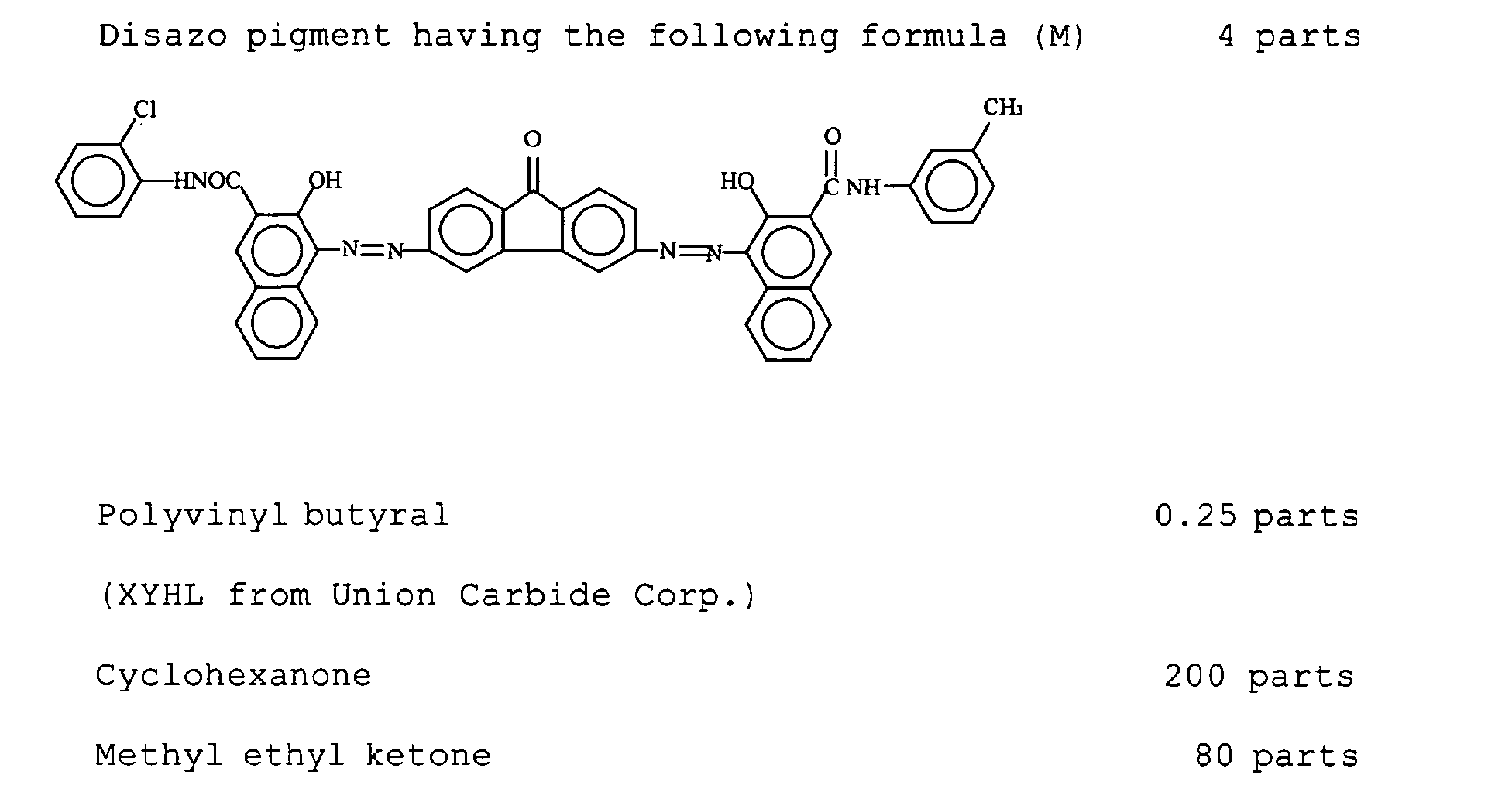
-
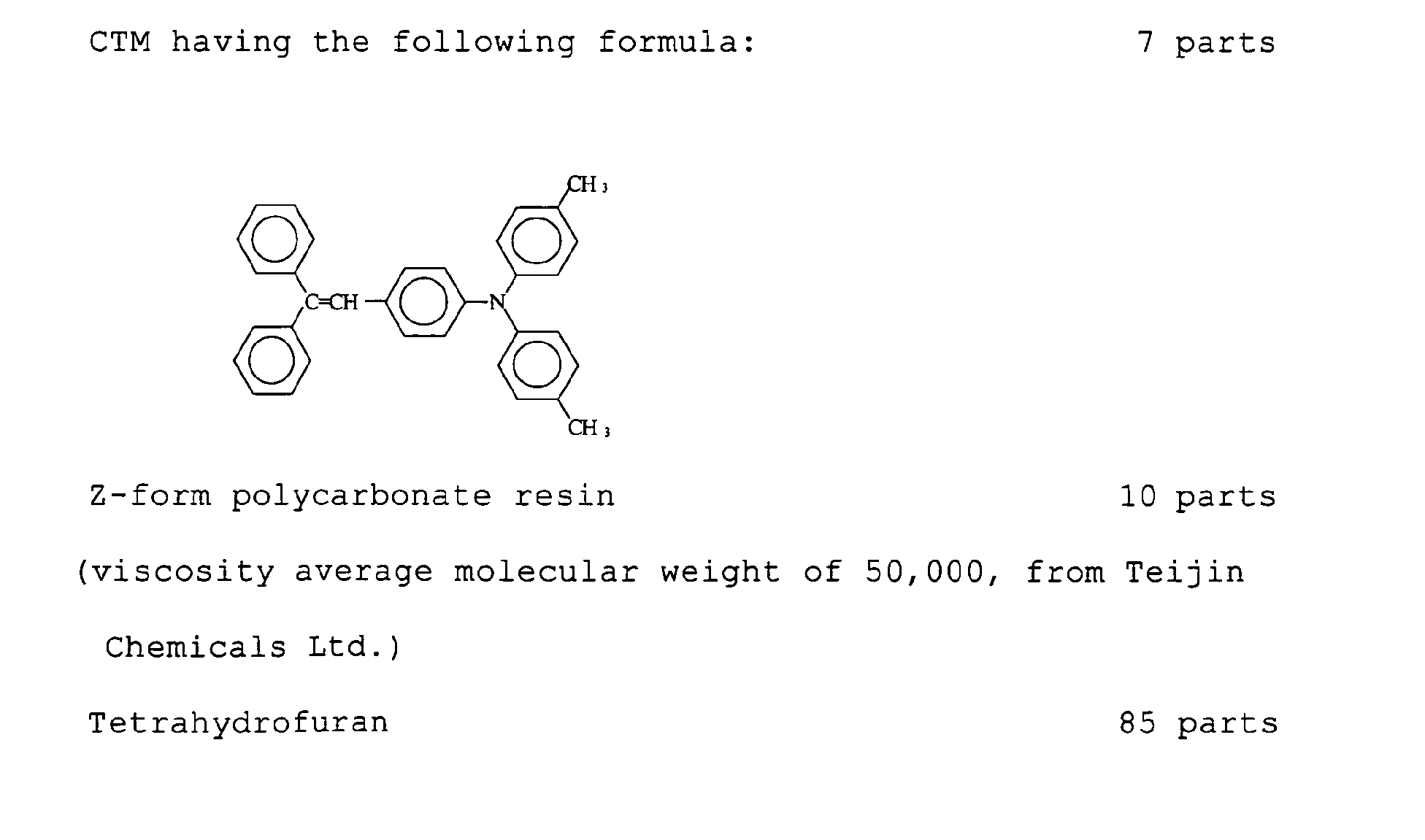

- On an aluminum cylinder with a diameter of 30 mm, the undercoat layer coating liquid, the CGL coating liquid and the CTL coating liquid mentioned above were coated and formed accordingly by a dip coating method and then dried.
- The elevating speed was controlled such that the undercoat layer was formed to have a thickness of 4.5 µm, the CGL was formed such that the light transmittance T (%) thereof for a light source wavelength of 655 nm was 45 % and the CTL was formed to have a thickness of 31 µm.
- The thus prepared photoreceptor was finished for practical use and evaluated as in Example 1. Thus Examples 8 to 11 and Comparative Examples 9 to 12 were performed.
- The evaluation results are shown in Table 3.
- The electrophotographic photoreceptor of Example 17 was prepared in the same manner as in Example 16 except that the CTL was formed to have a thickness of 20 µm.
- The thus prepared electrophotographic photoreceptor was evaluated in the same way as in Example 16.
- The evaluation results are shown in Table 3.
- The electrophotographic photoreceptor of Example 18 was prepared in the same manner as in Example 16 except that the CTL was formed to have a thickness of 33 µm.
- The thus prepared electrophotographic photoreceptor was evaluated in the same way as in Example 16.
- The evaluation results are shown in Table 3.
- The electrophotographic photoreceptor of Example 19 was prepared in the same manner as in Example 16 except that the CTL was formed to have a thickness of 16 µm.
- The thus prepared electrophotographic photoreceptor was evaluated in the same way as in Example 16.
- The evaluation results are shown in Table 3.
- The electrophotographic photoreceptor of Example 20 was prepared in the same manner as in Example 16 except that the light transmittance T (%) of the CGL for a light source wavelength of 655 nm was 36 %.
- The thus prepared electrophotographic photoreceptor was valuated in the same way as in Example 16.
- The evaluation results are shown in Table 3.
- The electrophotographic photoreceptor of Example 21 was prepared in the same manner as in Example 16 except that the light transmittance T (%) of the CGL for a light source wavelength of 655 nm was 39.2 %.
- The thus prepared electrophotographic photoreceptor was valuated in the same way as in Example 16.
- The evaluation results are shown in Table 3.
- The electrophotographic photoreceptor of Example 22 was prepared in the same manner as in Example 16 except that the light transmittance T (%) of the CGL for a light source wavelength of 655 nm was 41 %.
- The thus prepared electrophotographic photoreceptor was valuated in the same way as in Example 16.
- The evaluation results are shown in Table 3.
- The electrophotographic photoreceptor of Example 23 was prepared in the same manner as in Example 16 except that the light transmittance T (%) of the CGL for a light source wavelength of 655 nm was 54.1 %.
- The thus prepared electrophotographic photoreceptor was valuated in the same way as in Example 16.
- The evaluation results are shown in Table 3.
- The electrophotographic photoreceptor of Example 24 was prepared in the same manner as in Example 16 except that the light transmittance T (%) of the CGL for a light source wavelength of 655 nm was 55.6 %.
- The thus prepared electrophotographic photoreceptor was valuated in the same way as in Example 16.
- The evaluation results are shown in Table 3.
- The electrophotographic photoreceptor of Example 25 was prepared in the same manner as in Example 16 except that the light transmittance T (%) of the CGL for a light source wavelength of 655 nm was 64.3 %.
- The thus prepared electrophotographic photoreceptor was valuated in the same way as in Example 16.
- The evaluation results are shown in Table 3.
- The electrophotographic photoreceptor of Comparative Example 13 was prepared in the same manner as in Example 16 except that 4 parts by weight of Y form titanyl phtalocyanine was used in place of the disazo pigment used to prepare the CGL coating liquid in Example 16.
- The thus prepared electrophotographic photoreceptor was evaluated in the same way as in Example 16.
- The evaluation results are shown in Table 3.
- The electrophotographic photoreceptor of Comparative Example 14 was prepared in the same manner as in Example 16 except that the light transmittance T (%) of the CGL for a light source wavelength of 655 nm was 28 %.
- The thus prepared electrophotographic photoreceptor was evaluated in the same way as in Example 16.
- The evaluation results are shown in Table 3.
- The electrophotographic photoreceptor of Comparative Example 15 was prepared in the same manner as in Example 16 except the light transmittance T (%) of the CGL for a light source wavelength of 655 nm was 70 %.
- The thus prepared electrophotographic photoreceptor was evaluated in the same way as in Example 16.
- The evaluation results are shown in Table 3.
- The electrophotographic photoreceptor of Comparative Example 16 was prepared in the same manner as in Example 16 except that the CTL was formed to have a thickness of 13 µm.
- The thus prepared electrophotographic photoreceptor was evaluated in the same way as in Example 16.
- The evaluation results are shown in Table 3.
- The electrophotographic photoreceptor of Comparative Example 17 was prepared in the same manner as in Example 16 except that the light transmittance T (%) of the CGL for a light source wavelength of 655 nm was 34.5 %.
- The thus prepared electrophotographic photoreceptor was evaluated in the same way as in Example 16.
- The evaluation results are shown in Table 3.
- The electrophotographic photoreceptor of Comparative Example 18 was prepared in the same manner as in Example 16 except that the light transmittance T (%) of the CGL for a light source wavelength of 655 nm was 66 %.
- The thus prepared electrophotographic photoreceptor was evaluated in the same way as in Example 16.
- The evaluation results are shown in Table 3.
Electric Field Intensity (V/µm) Light Transmittance of the CGL Residual image evaluation (rank) Abnormal Image quality Writing wavelength % Example 16 16.1 655 nm 45 5 None Example 17 25.0 655 nm 45 5 None Example 18 15.1 655 nm 45 5 None Example 19 31.3 655 nm 45 5 None Example 20 16.1 655 nm 36 3 None Example 21 16.1 655 nm 39.2 4 None Example 22 16.1 655 nm 41 5 None Example 23 16.1 655 nm 54.1 5 None Example 24 16.1 655 nm 55.6 4 None Example 25 16.1 655 nm 64.3 3 None Comparative Example 13 16.1 655 nm 45 1 Residual Image Comparative Example 14 16.1 655 nm 28 1 Residual Image Comparative Example 15 16.1 655 nm 70 1 Residual Image Comparative Example 16 38.5 655 nm 45 2 Image density decrease Comparative Example 17 16.1 655 nm 34.5 2 Residual Image Comparative Example 18 16.1 655 nm 66 2 Residual Image - As seen in Table 3, high quality images free from residual and abnormal images were obtained in Examples satisfying the requirement of the present invention. To the contrary, in every Comparative Example, which did not satisfy the requirement of the present invention, abnormal images such as residual images and decrease in image density were observed.
- The photoreceptor of Example 16 was finished for practical use and then evaluated as in Example 9. Thus Example 26 was performed.
- The evaluation results are shown in Table 4.
- The test was performed in the same manner as in Example 26 for the electrophotographic photoreceptors of Example 17, 18 and 20 to 25. Thus Examples 27 to 34 were performed. The evaluation results are shown in Table 4.
- The test was performed in the same manner as in Example 26 for the electrophotographic photoreceptors of Comparative Examples 13 to 18. Thus Comparative Examples 19 to 24 were performed. The results are shown in Table 4.
Electric Field Intensity (V/µm) Light transmittance of the CGL Residual image evaluation (rank) Abnormal Image quality Writing wavelength % Example 26 22.6 655 nm 45 5 None Example 27 35.0 655 nm 45 5 None Example 28 21.2 655 nm 45 5 None Example 29 22.6 655 nm 36 3 None Example 30 22.6 655 nm 39.2 4 None Example 31 22.6 655 nm 41 5 None Example 32 22.6 655 nm 54.1 5 None Example 33 22.6 655 nm 55.6 4 None Example 34 22.6 655 nm 64.3 3 None Comparative Example 19 22.6 655 nm 45 1 Residual Image Comparative Example 20 22.6 655 nm 28 1 Residual Image Comparative Example 21 22.6 655 nm 70 1 Residual Image Comparative Example 22 53.8 655 nm 45 2 Image density decrease Comparative Example 23 22.6 655 nm 34.5 2 Residual Image Comparative Example 24 22.6 655 nm 66 2 Residual Image - As seen in Table 4, high quality images free from residual and abnormal images were obtained in Examples satisfying the requirement of the present invention. To the contrary, in every Comparative Example, which did not satisfy the requirement of the present invention, abnormal images such as residual images, background fouling and decrease in image density were observed.
- As mentioned above, since the electrophotographic apparatus of the present invention is capable of producing quality images free from abnormal image problems such as residual images, background fouling and decrease in image density, the electrophotographic apparatus of the present invention has a practical value for photocopiers, facsimile machines, laser printers, direct digital plate making machines, etc.
- This document claims priority and contains subject matter related to Japanese Patent Applications No. 2003-324986 and 2003-391070, filed on September 17, 2003, and November 20, 2003, respectively.
Claims (17)
- An electrophotographic photoreceptor (1; 11; 21; 31; 51; 71) comprising:wherein, when the charge generation layer (102) is irradiated with light having a highest reflectivity for the charge generation layer (102) in a range of from 360 nm to 740 nm after the undercoat layer (104) and the charge generation layer (102) are formed overlying the conductive substrate (101), the charge generation layer(102) has a reflectivity of from 15 to 21 %.a conductive substrate (101);an undercoat layer (104) located overlying the conductive substrate (101);a photosensitive layer located overlying the undercoat layer (104) and comprising:a charge generation layer (102 ) located overlying the undercoat layer (104); anda charge transport layer (103) located overlying the charge generation layer (102),
- The electrophotographic photoreceptor (1; 11; 21; 31; 51; 71) according to Claim 1, wherein the charge generation layer (102) comprises a disazo pigment represented by the following formula (I):wherein, A and B represent coupler remaining groups represented by the following formulae (II) to (VIII);
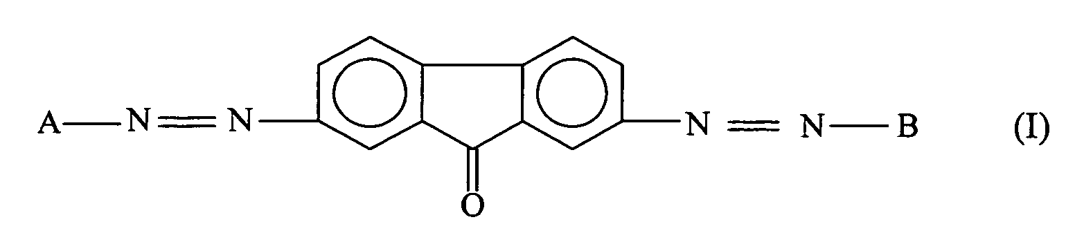 wherein, X1 represents -OH, -NHCOCH3, and -NHSO2CH3, Y1 represents -CON (R2) (R3), -CONHN = C(R6)(R7), -CONHN(R8) (R9) , -CONHCONH (R12) , a hydrogen atom, COOH, -COOCH3, COOC6H5 and a benzimidazol group, wherein R2 and R3 independently represent a hydrogen atom, a substituted or non-substituted alkyl group, a substituted or non-substituted aryl group and a substituted or non-substituted heterocyclic group or wherein R2 and R3 when taken together can form a ring with the nitrogen atom they are bonded to, R6 and R7 independently represent a hydrogen atom, a substituted or non-substituted alkyl group, a substituted or non-substituted aralkyl group, a substituted or non-substituted aryl group, a substituted or non-substituted styryl group and a substituted or non-substituted heterocyclic group or wherein R6 and R7 when taken together can form a ring with the nitrogen atom they are bonded to, R8 and R9 independently represent a hydrogen atom, a substituted or non-substituted alkyl group, a substituted or non-substituted aralkyl group, a substituted or non-substituted aryl group, a substituted or non-substituted styryl group and a substituted or non-substituted heterocyclic group or wherein R8 and R9 when taken together with the carbon atom they are bonded to can form a five-membered ring or six-membered ring optionally having a condensed aromatic ring, and R12 represents a substituted or non-substituted alkyl group, a substituted or non-substituted aryl group and a substituted or non-substituted heterocyclic group, and Z represents a remaining group which is fused with the benzene ring to form a polycyclic aromatic structure or a heterocyclic structure selected from the group consisting of a naphthalene ring, an anthracene ring, a carbazole ring, a benzocarbazole ring, a dibenzocarbazole ring, a dibenzofuran ring, a benzonaphthofuran ring and a dibenzothiophene ring, each of which can have at least one substituent;
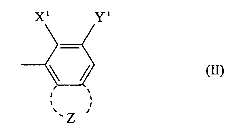 wherein R4 represents a hydrogen atom, a substituted or non-substituted alkyl group, and a substituted or non-substituted aryl group;
 wherein R5 represents a hydrogen atom, a substituted or non-substituted alkyl group, and a substituted or non-substituted aryl group;
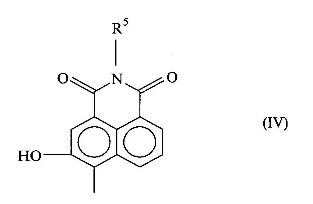 wherein Y represents a divalent aromatic hydrocarbon group or wherein Y together with the N-atoms it is bonded to forms a heterocyclic group;
 wherein Y represents a divalent aromatic hydrocarbon or wherein Y together with the N-atoms it is bonded to forms a heterocyclic group;
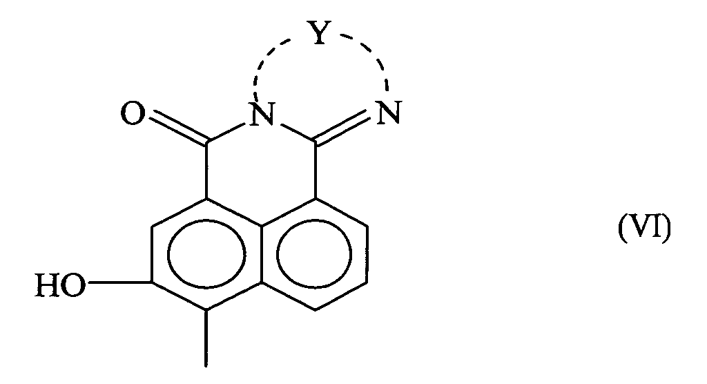 wherein R10 represents a hydrogen atom, an alkyl group, a carboxyl group, and a carboxyester group and Ar1 is a substituted or non-substituted aromatic hydrocarbon group; and
 wherein R11 represents a hydrogen atom, an alkyl group, a carboxyl group, and a carboxyester and Ar2 is a substituted or non-substituted aromatic hydrocarbon group.
- The electrophotographic photoreceptor (1; 11; 21; 31; 51; 71) according to Claim 1 or 2, wherein the charge generation layer (102) comprises a disazo pigment represented by the following formula (1)

- The electrophotographic photoreceptor (1; 11; 21; 31; 51; 71) according to any one of Claims 1 to 3, wherein the charge generation layer (102) has a reflectivity of from 17 to 19 %.
- An electrophotographic apparatus (100; 200; 300; 400; 500; 600) comprising:wherein the electrophotographic photoreceptor (1; 11; 21; 31; 51; 71) satisfies the following relationship:the electrophotographic photoreceptor (1; 11; 21; 31; 51; 71) of any one of Claims 1 to 4;a charger (2; 12; 22; 32; 52; 72) configured to uniformly charge a surface of the photoreceptor (1; 11; 21; 31; 51; 71);an image irradiator (3; 13; 23; 33; 53; 73) configured to irradiate the uniformly charged electrophotographic photoreceptor (1; 11; 21; 31; 51; 71) with light to form a latent electrostatic image thereon;a developing device (4; 14; 24; 34; 54; 74) configured to develop the latent electrostatic image with a toner (5);a transfer device (6; 16; 26; 36; 46; 56; 76) configured to transfer the developed image to a receiving material (8; 28; 38; 58; 78); anda cleaner (7; 17; 27; 37; 57; 77) configured to remove any toner remaining on the photoreceptor (1; 11; 21; 31; 51; 71),12 (V/µm) ≤ electric field intensity (V/D) ≤ 35 (V/µm),
wherein D (µm) represents a thickness of the charge transport layer (103) of the electrophotographic photoreceptor (1; 11; 21; 31; 51; 71) and V (V) represents an absolute potential of the surface of the electrophotographic photoreceptor (1; 11; 21; 31; 51; 71) due to charging. - The electrophotographic apparatus (100; 200; 300; 400; 500; 600) according to Claim 5, wherein the electrophotographic photoreceptor (1; 11; 21; 31; 51; 71) satisfies the following relationship:
- The electrophotographic apparatus (100; 200; 300; 400; 500; 600) according to Claim 5 or 6, wherein the toner (5) for use in developing the latent electrostatic image has a sphere form.
- The electrophotographic apparatus (100; 200; 300; 400; 500; 600) according to any one of Claims 5 to 7, further comprising:an intermediate transfer device (40; 80) to which multiple separate color toner images developed on the electrophotographic photoreceptor (1; 11; 21; 31; 51; 71) with separate color toners are transferred in a first step to form an overlaid color toner image on the intermediary transfer device (40; 80) while overlaying the separate color images thereon and from which the overlaid color toner image is transferred in a second step to the receiving material (8; 28; 38; 58; 78).
- A process cartridge (300), comprising:the electrophotographic photoreceptor (1; 11; 21; 31; 51; 71) of any one of Claims 1 to 4; and at least one ofa charger (2; 12; 22; 32; 52; 72) configured to uniformly charge a surface of the electrophotographic photoreceptor (1; 11; 21; 31; 51; 71);an image irradiator (3; 13; 23; 33; 53; 73) configured to irradiate the uniformly charged electrophotographic photoreceptor (1; 11; 21; 31; 51; 71) with light to form a latent electrostatic image thereon;a developing device (4; 14; 24; 34; 54; 74) configured to develop the latent electrostatic image with a toner (5);a transfer device (6, 16; 26; 36; 46; 56; 76) configured to transfer the developed image to a receiving material (8; 28; 38; 58; 78);a cleaner (7; 17; 27; 37; 57; 77) configured to remove any toner remaining on the electrophotographic photoreceptor (1; 11; 21; 31; 51; 71); anda quencher (30) configured to discharge the surface of the electrophotographic photoreceptor (1; 11; 21; 31; 51; 71).
- An electrophotgraphic apparatus (100; 200; 300; 400; 500; 600), comprising:wherein the electrophotographic photoreceptor (1; 11; 21; 31; 51; 71) satisfies the following relationship:an electrophotographic photoreceptor (1; 11; 21; 31; 51; 71) comprising:a conductive substrate (101);an undercoat layer (104) located overlying the conductive substrate (101);a photosensitive layer located overlying the undercoat layer (104) and comprising:a charge generation layer (102) located overlying the undercoat layer (104) comprising a disazo pigment and having a light transmittance of from 35 to 65 % against light to form a latent electrostatic image on the electrophotographic photoreceptor (1; 11; 21; 31; 51; 71); anda charge transport layer (103) located overlying the charge generation layer (102);a charger (2; 12; 22; 32; 52; 72) configured to uniformly charge a surface of the electrophotographic photoreceptor (1; 11; 21; 31; 51; 71);an image irradiator (3; 13; 23; 33; 53; 73) configured to irradiate the uniformly charged electrophotographic photoreceptor (1; 11; 21; 31; 51; 71) with the light to form a latent electrostatic image thereon;a developing device (4; 14; 24; 34; 54; 74) configured to develop the latent electrostatic image with a toner (5);a transfer device (6, 16; 26; 36; 46; 56; 76) configured to transfer the developed image to a receiving material (8; 28; 38; 58; 78) anda cleaner (7; 17; 27; 37; 57; 77) configured to remove any toner remaining on the electrophotographic photoreceptor (1; 11; 21; 31; 51; 71),
wherein the disazo pigment is represented by the following formula (I):wherein, A and B represent coupler remaining groups represented by the following formulae (II) to (VIII); wherein, X1 represents -OH, -NHCOCH3, and -NHSO2CH3, Y1 represents -CON(R2)(R3), -CONHN = C (R6) (R7) , -CONHN(R8) (R9), -CONHCONH(R12), a hydrogen atom, COOH, -COOCH3, COOC6H5 and a benzimidazol group, wherein R2 and R3 independently represent a hydrogen atom, a substituted or non-substituted alkyl group, a substituted or non-substituted aryl group and a substituted or non-substituted heterocyclic group or wherein R2 and R3 when taken together can form a ring with the nitrogen atom they are bonded to, R6 and R7 independently represent a hydrogen atom, a substituted or non-substituted alkyl group, a substituted or non-substituted aralkyl group, a substituted or non-substituted aryl group, a substituted or non-substituted styryl group and a substituted or non-substituted heterocyclic group or wherein R6 and R7 when taken together can form a ring with the nitrogen atom they are bonded to, R8 and R9 independently represent a hydrogen atom, a substituted or non-substituted alkyl group, a substituted or non-substituted aralkyl group, a substituted or non-substituted aryl group, a substituted or non-substituted styryl group and a substituted or non-substituted heterocyclic group or wherein R8 and R9 when taken together with the carbon atom they are bonded to can form a five-membered ring or six-membered ring optionally having a condensed aromatic ring, and R12 represents a substituted or non-substituted alkyl group, a substituted or non-substituted aryl group and a substituted or non-substituted heterocyclic group, and Z represents a remaining group which is fused with the benzene ring to form a polycyclic aromatic structure or a heterocyclic structure selected from the group consisting of a naphthalene ring, an anthracene ring, a carbazole ring, a benzocarbazole ring, a dibenzocarbazole ring, a dibenzofuran ring, a benzonaphthofuran ring and a dibenzothiophene ring, each of which can have at least one substituent;
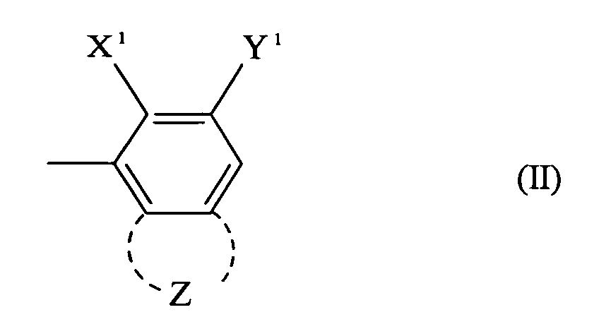 wherein R4 represents a hydrogen atom, a substituted or non-substituted alkyl group, and a substituted or non-substituted aryl group;
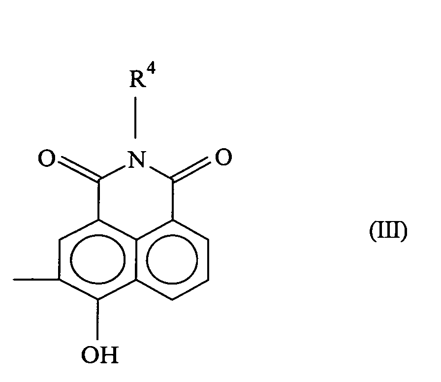 wherein R5 represents a hydrogen atom, a substituted or non-substituted alkyl group, and a substituted or non-substituted aryl group;
 wherein Y represents a divalent aromatic hydrocarbon group or wherein Y together with the N-atoms it is bonded to forms a heterocyclic group;
 wherein Y represents a divalent aromatic hydrocarbon or wherein Y together with the N-atoms it is bonded to forms a heterocyclic group;
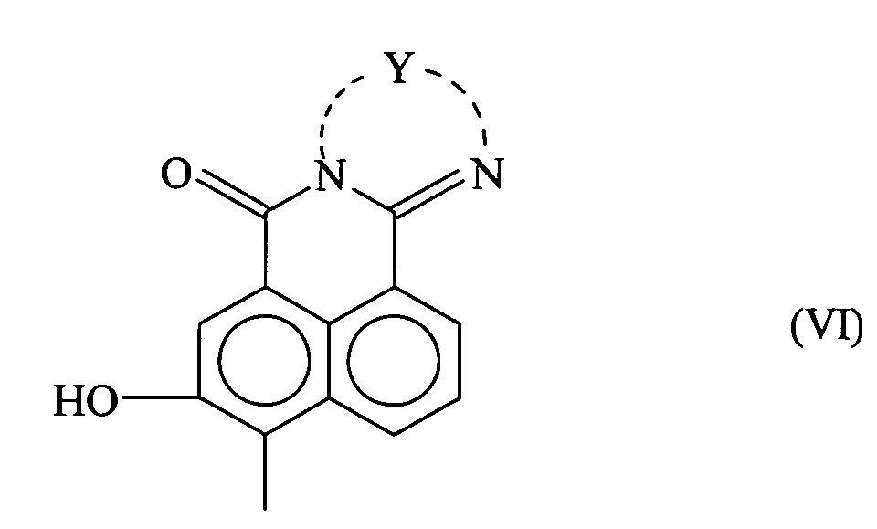 wherein R10 represents a hydrogen atom, an alkyl group, a carboxyl group, and a carboxyester group and Ar1 is a substituted or non-substituted aromatic hydrocarbon group; and
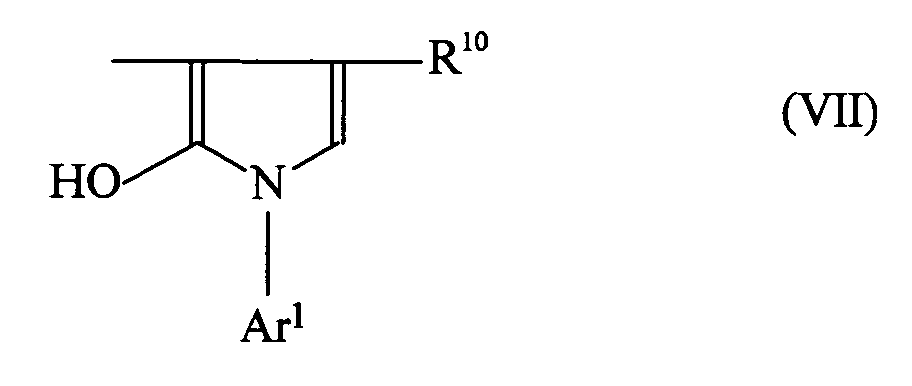 wherein R11 represents a hydrogen atom, an alkyl group, a carboxyl group, and a carboxyester and Ar2 is a substituted or non-substituted aromatic hydrocarbon group.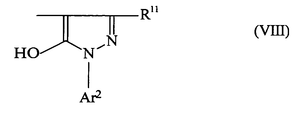
- The electrophotographic apparatus (100; 200; 300; 400; 500; 600) according to Claim 10, wherein the charge generation layer (102) includes a disazo pigment represented by the following formula (1).
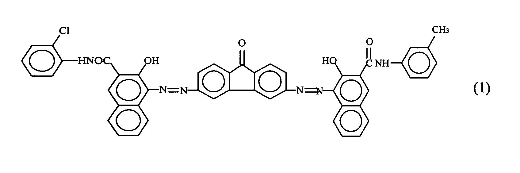
- The electrophotographic apparatus (100; 200; 300; 400; 500; 600) according to Claim 10 or 11, wherein the charge generation layer (102) has a light transmittance of from 40 to 55 %.
- The electrophotographic apparatus (100; 200; 300; 400; 500; 600) according to any one of Claims 10 to 12, wherein the electrophotographic photoreceptor (1; 11; 21; 31; 51; 71) satisfies the following relationship:
- The electrophotographic apparatus (100; 200; 300; 400; 500; 600) according to any one of Claims 10 to 13, wherein the toner (5) for use in developing the latent electrostatic image has a sphere form.
- The electrophotographic apparatus (100; 200; 300; 400; 500; 600) according to any one of Claims 10 to 14, further comprising:an intermediate transfer device (40; 80) to which multiple separate color toner images developed on the electrophotographic photoreceptor (1; 11; 21; 31; 51; 71) with separate color toners are transferred in a first step to form an overlaid color toner image on the intermediary transfer device (40; 80) while overlaying the separate color images thereon and from which the overlaid color toner image is transferred in a second step to the receiving material (8; 28; 38; 58; 78).
- A process cartridge (300) comprising:wherein the electrophotographic photoreceptor (1; 11; 21; 31; 51; 71) satisfies the following relationship:an electrophotographic photoreceptor (1; 11; 21; 31; 51; 71) comprising:a conductive substrate (101);an undercoat layer (104) located overlying the conductive substrate (101);a photosensitive layer located overlying the undercoat layer (104) comprising:a charge generation layer (102) located overlying the undercoat layer (104) and comprising a disazo pigment and having a light transmittance of from 35 to 65 % against light to form a latent electrostatic image on the electrophotographic photoreceptor (1; 11; 21; 31; 51; 71); anda charge transport layer (103) located overlying the charge generation layer (102);an image irradiator (3; 13; 23; 33; 53; 73) configured to irradiate the uniformly charged electrophotographic photoreceptor (1; 11; 21; 31; 51; 71) with the light to form a latent electrostatic image thereon;a charger (2; 12; 22; 32; 52; 72) configured to uniformly charge a surface of the electrophotographic photoreceptor (1; 11; 21; 31; 51; 71); and at least one ofa developing device (4; 14; 24; 34; 54; 74) configured to develop the latent electrostatic image with a toner (5);a transfer device (6, 16; 26; 36; 46; 56; 76) configured to transfer the developed image to a receiving material(8; 28; 38; 58; 78);a cleaner (7; 17; 27; 37; 57; 77) configured to remove any toner remaining on the electrophotographic photoreceptor (1; 11; 21; 31; 51; 71); anda quencher (30) configured to discharge the surface of the electrophotographic photoreceptor (1; 11; 21; 31; 51; 71),
wherein the disazo pigment is represented by the following formula (I):wherein, A and B represent coupler remaining groups represented by the following formulae (II) to (VIII); wherein, X1 represents -OH, -NHCOCH3, and -NHSO2CH3, Y1 represents -CON (R2) (R3) , -CONHN = C(R6) (R7), -CONHN(R8) (R9), -CONHCONH(R12), a hydrogen atom, COOH, -COOCH3, COOC6H5 and a benzimidazol group, wherein R2 and R3 independently represent a hydrogen atom, a substituted or non-substituted alkyl group, a substituted or non-substituted aryl group and a substituted or non-substituted heterocyclic group or wherein R2 and R3 when taken together can form a ring with the nitrogen atom they are bonded to, R6 and R7 independently represent a hydrogen atom, a substituted or non-substituted alkyl group, a substituted or non-substituted aralkyl group, a substituted or non-substituted aryl group, a substituted or non-substituted styryl group and a substituted or non-substituted heterocyclic group or wherein R6 and R7 when taken together can form a ring with the nitrogen atom they are bonded to, R8 and R9 independently represent a hydrogen atom, a substituted or non-substituted alkyl group, a substituted or non-substituted aralkyl group, a substituted or non-substituted aryl group, a substituted or non-substituted styryl group and a substituted or non-substituted heterocyclic group or wherein R8 and R9 when taken together with the carbon atom they are bonded to can form a five-membered ring or six-membered ring optionally having a condensed aromatic ring, and R12 represents a substituted or non-substituted alkyl group, a substituted or non-substituted aryl group and a substituted or non-substituted heterocyclic group, and Z represents a remaining group which is fused with the benzene ring to form a polycyclic aromatic structure or a heterocyclic structure selected from the group consisting of a naphthalene ring, an anthracene ring, a carbazole ring, a benzocarbazole ring, a dibenzocarbazole ring, a dibenzofuran ring, a benzonaphthofuran ring and a dibenzothiophene ring, each of which can have at least one substituent;
 wherein R4 represents a hydrogen atom, a substituted or non-substituted alkyl group, and a substituted or non-substituted aryl group;
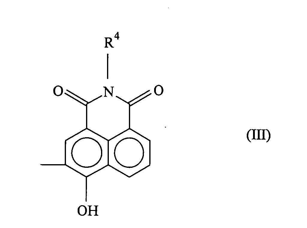 wherein R5 represents a hydrogen atom, a substituted or non-substituted alkyl group, and a substituted or non-substituted aryl group;
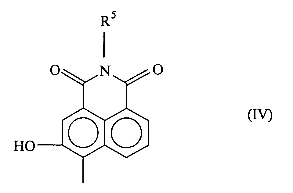 wherein Y represents a divalent aromatic hydrocarbon group or wherein Y together with the N-atoms it is bonded to forms a heterocyclic group;
 wherein Y represents a divalent aromatic hydrocarbon or wherein Y together with the N-atoms it is bonded to forms a heterocyclic group;
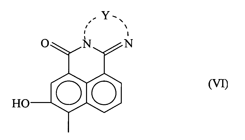 wherein R10 represents a hydrogen atom, an alkyl group, a carboxyl group, and a carboxyester group and Ar1 is a substituted or non-substituted aromatic hydrocarbon group; and
 wherein R11 represents a hydrogen atom, an alkyl group, a carboxyl group, and a carboxyester and Ar2 is a substituted or non-substituted aromatic hydrocarbon group.
- A method of manufacturing an electrophotographic
photoreceptor (1; 11; 21; 31; 51; 71), comprising:wherein, when the charge generation layer is irradiated with light having a highest reflectivity for the charge generation layer (102) in a range of from 360 nm to 740 nm after the undercoat layer (104) and the charge generation layer (102) are formed overlying the conductive substrate (101), the charge generation layer (102) has a reflectivity of from 15 to 21 %.forming a conductive substrate (101);forming an undercoat layer (104) located overlying the conductive substrate (101) andforming a charge generation layer (102) located overlying the undercoat layer (104); andforming a charge transport layer (103) located overlying the charge generation layer (102),
Applications Claiming Priority (4)
| Application Number | Priority Date | Filing Date | Title |
|---|---|---|---|
| JP2003324986 | 2003-09-17 | ||
| JP2003324986 | 2003-09-17 | ||
| JP2003391070 | 2003-11-20 | ||
| JP2003391070 | 2003-11-20 |
Publications (2)
| Publication Number | Publication Date |
|---|---|
| EP1521124A1 true EP1521124A1 (en) | 2005-04-06 |
| EP1521124B1 EP1521124B1 (en) | 2008-10-08 |
Family
ID=34277752
Family Applications (1)
| Application Number | Title | Priority Date | Filing Date |
|---|---|---|---|
| EP04022182A Expired - Lifetime EP1521124B1 (en) | 2003-09-17 | 2004-09-17 | Electrophotographic photoreceptor, method of manufacturing electrophotographic photoreceptor, and electrophotographic apparatus and process cartridge using electrophotographic photoreceptor |
Country Status (4)
| Country | Link |
|---|---|
| US (1) | US7341810B2 (en) |
| EP (1) | EP1521124B1 (en) |
| DE (1) | DE602004016930D1 (en) |
| ES (1) | ES2315605T3 (en) |
Families Citing this family (15)
| Publication number | Priority date | Publication date | Assignee | Title |
|---|---|---|---|---|
| EP1712956A3 (en) * | 2005-04-13 | 2007-05-30 | Ricoh Company, Ltd. | Image bearing member, and image forming apparatus and process cartridge using the same |
| JP2007033911A (en) * | 2005-07-27 | 2007-02-08 | Oki Data Corp | Image forming apparatus |
| JP4570045B2 (en) * | 2005-08-18 | 2010-10-27 | 株式会社リコー | Electrophotographic photosensitive member, electrophotographic apparatus, and process cartridge for electrophotographic apparatus |
| EP1762899B1 (en) * | 2005-09-12 | 2008-10-29 | Ricoh Company, Ltd. | Latent electrostatic image bearing member, and the method for producing the same, image forming method, image forming apparatus, and process cartridge |
| US8192905B2 (en) * | 2006-04-20 | 2012-06-05 | Ricoh Company, Ltd. | Electrophotographic photoconductor, image forming apparatus, and process cartridge |
| KR20080005734A (en) * | 2006-07-10 | 2008-01-15 | 삼성전자주식회사 | Organophotoreceptor and electrophotographic image forming apparatus employing the same |
| JP2008096537A (en) * | 2006-10-06 | 2008-04-24 | Ricoh Co Ltd | Cleaning device, process cartridge, and image forming apparatus |
| US7768105B2 (en) * | 2007-01-24 | 2010-08-03 | Fairchild Semiconductor Corporation | Pre-molded clip structure |
| JP4801607B2 (en) * | 2007-03-06 | 2011-10-26 | 株式会社リコー | Image forming method and image forming apparatus |
| JP4825167B2 (en) * | 2007-05-11 | 2011-11-30 | 株式会社リコー | Electrophotographic photosensitive member, image forming apparatus, and process cartridge |
| US8244145B2 (en) * | 2007-08-29 | 2012-08-14 | Ricoh Company, Ltd. | Image forming apparatus including image processing member determined by method of evaluating distribution of adhesion forces of toner thereto |
| US8263297B2 (en) * | 2007-11-28 | 2012-09-11 | Ricoh Company, Ltd. | Electrophotographic photoconductor and electrophotographic apparatus |
| US8380109B2 (en) | 2008-01-11 | 2013-02-19 | Ricoh Company, Ltd. | Image forming apparatus and process cartridge |
| JP2009300590A (en) * | 2008-06-11 | 2009-12-24 | Ricoh Co Ltd | Electrophotographic photoreceptor |
| JP6481324B2 (en) | 2013-12-13 | 2019-03-13 | 株式会社リコー | Electrophotographic photosensitive member, electrophotographic method, electrophotographic apparatus, and process cartridge |
Citations (3)
| Publication number | Priority date | Publication date | Assignee | Title |
|---|---|---|---|---|
| US5824444A (en) * | 1994-09-29 | 1998-10-20 | Konica Corporation | Image forming apparatus |
| US6337165B1 (en) * | 1999-12-27 | 2002-01-08 | Mitsubishi Chemical Corporation | Electrophotographic photoreceptor and process for producing the same |
| US20030059693A1 (en) * | 2001-03-23 | 2003-03-27 | Takaaki Ikegami | Electrophotographic image forming apparatus and process cartridge, and electrophotographic photoreceptor therefor |
Family Cites Families (49)
| Publication number | Priority date | Publication date | Assignee | Title |
|---|---|---|---|---|
| US4618672A (en) * | 1980-04-30 | 1986-10-21 | Ricoh Company, Ltd. | Bisazo compounds useful as charge generating pigments in electrophotography |
| US4400455A (en) * | 1980-12-10 | 1983-08-23 | Ricoh Company Ltd. | Layered organic electrophotographic photoconductor element comprising bisazo generating and hydrazone transport layers |
| US4481271A (en) * | 1980-12-15 | 1984-11-06 | Ricoh Company, Ltd. | Layered electrophotographic photoconductor containing a hydrazone |
| JPH06313972A (en) | 1993-04-28 | 1994-11-08 | Canon Inc | Electrophotographic photoreceptor and electrophotographic apparatus |
| JPH0713374A (en) | 1993-06-23 | 1995-01-17 | Canon Inc | Electrophotographic photoreceptor and electrophotographic apparatus having the same |
| JP3352166B2 (en) | 1993-07-30 | 2002-12-03 | キヤノン株式会社 | Electrophotographic photoreceptor, electrophotographic apparatus and apparatus unit having the same |
| JPH0744065A (en) | 1993-07-30 | 1995-02-14 | Canon Inc | Electrophotographic device |
| JPH0792701A (en) | 1993-07-30 | 1995-04-07 | Canon Inc | Electrophotographic photoreceptor, process cartridge having the electrophotographic photoreceptor, and electrophotographic apparatus |
| US5578405A (en) * | 1993-10-14 | 1996-11-26 | Ricoh Company | Electrophotographic photoconductor containing disazo and trisazo pigments |
| JPH0822136A (en) | 1994-07-04 | 1996-01-23 | Fuji Xerox Co Ltd | Electrophotographic method |
| JP3893632B2 (en) | 1994-09-29 | 2007-03-14 | コニカミノルタホールディングス株式会社 | Electrophotographic photoreceptor and image forming method and apparatus |
| JP2827937B2 (en) | 1994-11-22 | 1998-11-25 | 富士ゼロックス株式会社 | Electrophotographic photosensitive member having undercoat layer and electrophotographic apparatus |
| JP3607008B2 (en) * | 1995-08-09 | 2005-01-05 | 株式会社リコー | Electrophotographic photoreceptor |
| JP3139381B2 (en) | 1996-01-18 | 2001-02-26 | 富士電機株式会社 | Electrophotographic photoreceptor and method of manufacturing the same |
| JPH09211876A (en) | 1996-02-01 | 1997-08-15 | Fuji Xerox Co Ltd | Electrophotographic photoreceptor |
| JPH1073942A (en) | 1996-06-25 | 1998-03-17 | Fuji Electric Co Ltd | Electrophotographic photoreceptor |
| JPH1069104A (en) | 1996-08-26 | 1998-03-10 | Fuji Xerox Co Ltd | Electrophotographic photoreceptor and electrophotographic device |
| JPH10115946A (en) | 1996-10-09 | 1998-05-06 | Canon Inc | Electrophotographic photosensitive member, process cartridge provided with the electrophotographic photosensitive member, and electrophotographic apparatus |
| JP4076596B2 (en) | 1996-10-25 | 2008-04-16 | 富士ゼロックス株式会社 | Electrophotographic apparatus and image forming method |
| JPH10123856A (en) | 1996-10-25 | 1998-05-15 | Fuji Xerox Co Ltd | Electrophotographic device and image forming method |
| JPH10123855A (en) | 1996-10-25 | 1998-05-15 | Fuji Xerox Co Ltd | Electrophotographic device and image forming method |
| JPH10177269A (en) | 1996-12-18 | 1998-06-30 | Fuji Xerox Co Ltd | Electrophotographic device and image forming method |
| JPH10177262A (en) | 1996-12-18 | 1998-06-30 | Fuji Xerox Co Ltd | Electrophotographic device and image forming method |
| JPH10177263A (en) | 1996-12-18 | 1998-06-30 | Fuji Xerox Co Ltd | Electrophotographic device and image forming method |
| JPH10177261A (en) | 1996-12-18 | 1998-06-30 | Fuji Xerox Co Ltd | Electrophotographic device and image forming method |
| JP3554126B2 (en) | 1996-12-20 | 2004-08-18 | キヤノン株式会社 | Electrophotographic photoreceptor, process cartridge having the electrophotographic photoreceptor, and electrophotographic apparatus |
| JPH10246997A (en) | 1997-03-06 | 1998-09-14 | Canon Inc | Electrophotographic equipment |
| JPH11133825A (en) | 1997-10-29 | 1999-05-21 | Canon Inc | Image forming device |
| JPH11184127A (en) | 1997-12-24 | 1999-07-09 | Canon Inc | Electrophotographic photoreceptor, process cartridge and electrophotographic apparatus |
| JPH11184135A (en) | 1997-12-25 | 1999-07-09 | Canon Inc | Electrophotographic photoreceptor, process cartridge and electrophotographic apparatus |
| JP3715829B2 (en) | 1998-05-06 | 2005-11-16 | キヤノン株式会社 | Electrophotographic method and electrophotographic apparatus |
| JP4323629B2 (en) | 1998-07-31 | 2009-09-02 | キヤノン株式会社 | Electrophotographic equipment |
| JP2000112162A (en) | 1998-08-05 | 2000-04-21 | Canon Inc | Electrophotographic photoreceptor and method of manufacturing the same |
| JP2000075521A (en) | 1998-08-31 | 2000-03-14 | Canon Inc | Electrophotographic photoreceptor, process cartridge having the electrophotographic photoreceptor, and electrophotographic apparatus |
| JP2000147803A (en) | 1998-11-10 | 2000-05-26 | Fuji Xerox Co Ltd | Electrophotographic apparatus and image forming method |
| JP4250292B2 (en) | 1999-02-05 | 2009-04-08 | キヤノン株式会社 | Electrophotographic photosensitive member, process cartridge having the electrophotographic photosensitive member, and electrophotographic apparatus |
| JP2001051438A (en) | 1999-08-05 | 2001-02-23 | Canon Inc | Electrophotographic photoreceptor, manufacturing method thereof, process cartridge and electrophotographic apparatus |
| JP2001117244A (en) | 1999-10-18 | 2001-04-27 | Fuji Xerox Co Ltd | Digital electrophotographic device |
| JP2001235889A (en) | 2000-02-24 | 2001-08-31 | Fuji Xerox Co Ltd | Electrophotographic photoreceptor, electrophotographic device with the same, process cartridge and method for producing the electrophotographic photoreceptor |
| JP4093725B2 (en) * | 2000-04-05 | 2008-06-04 | 株式会社リコー | Electrophotographic photosensitive member, image forming method using the same, image forming apparatus, and process cartridge for image forming apparatus |
| JP3785021B2 (en) | 2000-04-19 | 2006-06-14 | 三菱化学株式会社 | Electrophotographic photoreceptor |
| JP4010739B2 (en) | 2000-04-19 | 2007-11-21 | 三菱化学株式会社 | Electrophotographic photosensitive member and electrophotographic method |
| JP4346793B2 (en) | 2000-06-21 | 2009-10-21 | キヤノン株式会社 | Electrophotographic photosensitive member, process cartridge, and electrophotographic apparatus |
| JP2002107983A (en) | 2000-09-29 | 2002-04-10 | Canon Inc | Electrophotographic photoreceptor, process cartridge and image forming apparatus |
| JP2002107972A (en) | 2000-10-02 | 2002-04-10 | Canon Inc | Electrophotographic photoreceptor, manufacturing method thereof, process cartridge and electrophotographic apparatus |
| JP2002123067A (en) | 2000-10-18 | 2002-04-26 | Fuji Xerox Co Ltd | Image forming method |
| JP3734735B2 (en) * | 2000-11-02 | 2006-01-11 | 株式会社リコー | Electrophotographic photoreceptor |
| EP1205808B1 (en) * | 2000-11-08 | 2010-03-17 | Ricoh Company, Ltd. | Electrophotographic photoreceptor and method of preparation thereof and image forming method and apparatus using the photoreceptor |
| JP3766008B2 (en) * | 2000-11-30 | 2006-04-12 | 株式会社リコー | Electrophotographic photosensitive member, method for producing the same, electrophotographic method, image forming apparatus, and process cartridge for image forming apparatus |
-
2004
- 2004-09-17 ES ES04022182T patent/ES2315605T3/en not_active Expired - Lifetime
- 2004-09-17 EP EP04022182A patent/EP1521124B1/en not_active Expired - Lifetime
- 2004-09-17 US US10/943,196 patent/US7341810B2/en not_active Expired - Lifetime
- 2004-09-17 DE DE602004016930T patent/DE602004016930D1/en not_active Expired - Lifetime
Patent Citations (3)
| Publication number | Priority date | Publication date | Assignee | Title |
|---|---|---|---|---|
| US5824444A (en) * | 1994-09-29 | 1998-10-20 | Konica Corporation | Image forming apparatus |
| US6337165B1 (en) * | 1999-12-27 | 2002-01-08 | Mitsubishi Chemical Corporation | Electrophotographic photoreceptor and process for producing the same |
| US20030059693A1 (en) * | 2001-03-23 | 2003-03-27 | Takaaki Ikegami | Electrophotographic image forming apparatus and process cartridge, and electrophotographic photoreceptor therefor |
Also Published As
| Publication number | Publication date |
|---|---|
| US20050058918A1 (en) | 2005-03-17 |
| EP1521124B1 (en) | 2008-10-08 |
| ES2315605T3 (en) | 2009-04-01 |
| DE602004016930D1 (en) | 2008-11-20 |
| US7341810B2 (en) | 2008-03-11 |
Similar Documents
| Publication | Publication Date | Title |
|---|---|---|
| EP1291723B1 (en) | Electrophotographic photoreceptor, and image forming method, image forming apparatus and process cartridge therefor using the photoreceptor | |
| US6596449B2 (en) | Electrophotographic photoreceptor, and process cartridge and electrophotographic image forming apparatus using the electrophotographic photoreceptor | |
| JP4030895B2 (en) | Electrophotographic photosensitive member, image forming method, image forming apparatus, and process cartridge for image forming apparatus | |
| EP1521124B1 (en) | Electrophotographic photoreceptor, method of manufacturing electrophotographic photoreceptor, and electrophotographic apparatus and process cartridge using electrophotographic photoreceptor | |
| JP2003262965A (en) | Image forming device | |
| US7270924B2 (en) | Electrophotographic photoreceptor, method for manufacturing the electrophotographic photoreceptor, and image forming apparatus and process cartridge using the electrophotographic photoreceptor | |
| US7223507B2 (en) | Imaging members | |
| JP4928230B2 (en) | Image forming apparatus, image forming method, and process cartridge | |
| US20030059693A1 (en) | Electrophotographic image forming apparatus and process cartridge, and electrophotographic photoreceptor therefor | |
| EP2146251B1 (en) | Electrophotographic photoconductor, image forming apparatus using the same, and process cartridge | |
| JP5277764B2 (en) | Electrophotographic photoreceptor, image forming apparatus using the same, and process cartridge | |
| CN100414439C (en) | Electrophotographic photoreceptor, manufacturing method, electrophotographic device, and process cartridge | |
| JP5391875B2 (en) | Electrophotographic photoreceptor, method for manufacturing the same, image forming apparatus, and process cartridge | |
| JP5545462B2 (en) | Electrophotographic photoreceptor, image forming apparatus using the same, and process cartridge | |
| JP5401933B2 (en) | Electrophotographic photoreceptor, image forming method using the electrophotographic photoreceptor, image forming apparatus, and process cartridge for image forming apparatus | |
| JPH1138654A (en) | Coating composition for electrophotographic photoreceptor, electrophotographic photoreceptor and its production | |
| JP2011090246A (en) | Electrophotographic photoreceptor, electrophotographic method, electrophotographic device, and process cartridge for electrophotographic device | |
| JP2005173557A (en) | Electrophotographic apparatus and process cartridge | |
| JP2001330976A (en) | Full color electrophotographic equipment | |
| JP4498178B2 (en) | Electrophotographic photosensitive member, manufacturing method, and electrophotographic apparatus | |
| JP3883454B2 (en) | Image forming apparatus | |
| JP3874329B2 (en) | Multilayer electrophotographic photoreceptor, image forming method, image forming apparatus, and process cartridge for image forming apparatus | |
| JP3883456B2 (en) | Image forming apparatus | |
| JP2001117249A (en) | Electrophotographic photoreceptor, electrophotographic method, electrophotographic apparatus, and process cartridge for electrophotographic apparatus | |
| JP2005115360A (en) | Electrophotographic apparatus and process cartridge |
Legal Events
| Date | Code | Title | Description |
|---|---|---|---|
| PUAI | Public reference made under article 153(3) epc to a published international application that has entered the european phase |
Free format text: ORIGINAL CODE: 0009012 |
|
| AK | Designated contracting states |
Kind code of ref document: A1 Designated state(s): AT BE BG CH CY CZ DE DK EE ES FI FR GB GR HU IE IT LI LU MC NL PL PT RO SE SI SK TR |
|
| AX | Request for extension of the european patent |
Extension state: AL HR LT LV MK |
|
| 17P | Request for examination filed |
Effective date: 20050512 |
|
| AKX | Designation fees paid |
Designated state(s): DE ES FR GB IT NL |
|
| GRAP | Despatch of communication of intention to grant a patent |
Free format text: ORIGINAL CODE: EPIDOSNIGR1 |
|
| GRAS | Grant fee paid |
Free format text: ORIGINAL CODE: EPIDOSNIGR3 |
|
| GRAA | (expected) grant |
Free format text: ORIGINAL CODE: 0009210 |
|
| AK | Designated contracting states |
Kind code of ref document: B1 Designated state(s): DE ES FR GB IT NL |
|
| REG | Reference to a national code |
Ref country code: GB Ref legal event code: FG4D |
|
| REF | Corresponds to: |
Ref document number: 602004016930 Country of ref document: DE Date of ref document: 20081120 Kind code of ref document: P |
|
| NLV1 | Nl: lapsed or annulled due to failure to fulfill the requirements of art. 29p and 29m of the patents act | ||
| REG | Reference to a national code |
Ref country code: ES Ref legal event code: FG2A Ref document number: 2315605 Country of ref document: ES Kind code of ref document: T3 |
|
| PG25 | Lapsed in a contracting state [announced via postgrant information from national office to epo] |
Ref country code: NL Free format text: LAPSE BECAUSE OF FAILURE TO SUBMIT A TRANSLATION OF THE DESCRIPTION OR TO PAY THE FEE WITHIN THE PRESCRIBED TIME-LIMIT Effective date: 20081008 |
|
| PLBE | No opposition filed within time limit |
Free format text: ORIGINAL CODE: 0009261 |
|
| STAA | Information on the status of an ep patent application or granted ep patent |
Free format text: STATUS: NO OPPOSITION FILED WITHIN TIME LIMIT |
|
| PG25 | Lapsed in a contracting state [announced via postgrant information from national office to epo] |
Ref country code: IT Free format text: LAPSE BECAUSE OF FAILURE TO SUBMIT A TRANSLATION OF THE DESCRIPTION OR TO PAY THE FEE WITHIN THE PRESCRIBED TIME-LIMIT Effective date: 20081008 |
|
| 26N | No opposition filed |
Effective date: 20090709 |
|
| REG | Reference to a national code |
Ref country code: FR Ref legal event code: PLFP Year of fee payment: 13 |
|
| REG | Reference to a national code |
Ref country code: FR Ref legal event code: PLFP Year of fee payment: 14 |
|
| PGFP | Annual fee paid to national office [announced via postgrant information from national office to epo] |
Ref country code: DE Payment date: 20170928 Year of fee payment: 14 Ref country code: GB Payment date: 20170921 Year of fee payment: 14 Ref country code: FR Payment date: 20170928 Year of fee payment: 14 |
|
| PGFP | Annual fee paid to national office [announced via postgrant information from national office to epo] |
Ref country code: ES Payment date: 20171026 Year of fee payment: 14 |
|
| REG | Reference to a national code |
Ref country code: DE Ref legal event code: R119 Ref document number: 602004016930 Country of ref document: DE |
|
| GBPC | Gb: european patent ceased through non-payment of renewal fee |
Effective date: 20180917 |
|
| PG25 | Lapsed in a contracting state [announced via postgrant information from national office to epo] |
Ref country code: DE Free format text: LAPSE BECAUSE OF NON-PAYMENT OF DUE FEES Effective date: 20190402 |
|
| PG25 | Lapsed in a contracting state [announced via postgrant information from national office to epo] |
Ref country code: FR Free format text: LAPSE BECAUSE OF NON-PAYMENT OF DUE FEES Effective date: 20180930 |
|
| PG25 | Lapsed in a contracting state [announced via postgrant information from national office to epo] |
Ref country code: GB Free format text: LAPSE BECAUSE OF NON-PAYMENT OF DUE FEES Effective date: 20180917 |
|
| REG | Reference to a national code |
Ref country code: ES Ref legal event code: FD2A Effective date: 20191031 |
|
| PG25 | Lapsed in a contracting state [announced via postgrant information from national office to epo] |
Ref country code: ES Free format text: LAPSE BECAUSE OF NON-PAYMENT OF DUE FEES Effective date: 20180918 |