EP1520712B1 - Druckkopf mit zwei tröpfchengrössen - Google Patents
Druckkopf mit zwei tröpfchengrössen Download PDFInfo
- Publication number
- EP1520712B1 EP1520712B1 EP04024987A EP04024987A EP1520712B1 EP 1520712 B1 EP1520712 B1 EP 1520712B1 EP 04024987 A EP04024987 A EP 04024987A EP 04024987 A EP04024987 A EP 04024987A EP 1520712 B1 EP1520712 B1 EP 1520712B1
- Authority
- EP
- European Patent Office
- Prior art keywords
- heater
- switch
- heaters
- substrate
- switching devices
- Prior art date
- Legal status (The legal status is an assumption and is not a legal conclusion. Google has not performed a legal analysis and makes no representation as to the accuracy of the status listed.)
- Expired - Lifetime
Links
Images


Classifications
-
- B—PERFORMING OPERATIONS; TRANSPORTING
- B41—PRINTING; LINING MACHINES; TYPEWRITERS; STAMPS
- B41J—TYPEWRITERS; SELECTIVE PRINTING MECHANISMS, i.e. MECHANISMS PRINTING OTHERWISE THAN FROM A FORME; CORRECTION OF TYPOGRAPHICAL ERRORS
- B41J2/00—Typewriters or selective printing mechanisms characterised by the printing or marking process for which they are designed
- B41J2/005—Typewriters or selective printing mechanisms characterised by the printing or marking process for which they are designed characterised by bringing liquid or particles selectively into contact with a printing material
- B41J2/01—Ink jet
- B41J2/205—Ink jet for printing a discrete number of tones
-
- B—PERFORMING OPERATIONS; TRANSPORTING
- B41—PRINTING; LINING MACHINES; TYPEWRITERS; STAMPS
- B41J—TYPEWRITERS; SELECTIVE PRINTING MECHANISMS, i.e. MECHANISMS PRINTING OTHERWISE THAN FROM A FORME; CORRECTION OF TYPOGRAPHICAL ERRORS
- B41J2/00—Typewriters or selective printing mechanisms characterised by the printing or marking process for which they are designed
- B41J2/005—Typewriters or selective printing mechanisms characterised by the printing or marking process for which they are designed characterised by bringing liquid or particles selectively into contact with a printing material
- B41J2/01—Ink jet
- B41J2/015—Ink jet characterised by the jet generation process
- B41J2/04—Ink jet characterised by the jet generation process generating single droplets or particles on demand
- B41J2/045—Ink jet characterised by the jet generation process generating single droplets or particles on demand by pressure, e.g. electromechanical transducers
- B41J2/04501—Control methods or devices therefor, e.g. driver circuits, control circuits
- B41J2/04533—Control methods or devices therefor, e.g. driver circuits, control circuits controlling a head having several actuators per chamber
-
- B—PERFORMING OPERATIONS; TRANSPORTING
- B41—PRINTING; LINING MACHINES; TYPEWRITERS; STAMPS
- B41J—TYPEWRITERS; SELECTIVE PRINTING MECHANISMS, i.e. MECHANISMS PRINTING OTHERWISE THAN FROM A FORME; CORRECTION OF TYPOGRAPHICAL ERRORS
- B41J2/00—Typewriters or selective printing mechanisms characterised by the printing or marking process for which they are designed
- B41J2/005—Typewriters or selective printing mechanisms characterised by the printing or marking process for which they are designed characterised by bringing liquid or particles selectively into contact with a printing material
- B41J2/01—Ink jet
- B41J2/015—Ink jet characterised by the jet generation process
- B41J2/04—Ink jet characterised by the jet generation process generating single droplets or particles on demand
- B41J2/045—Ink jet characterised by the jet generation process generating single droplets or particles on demand by pressure, e.g. electromechanical transducers
- B41J2/04501—Control methods or devices therefor, e.g. driver circuits, control circuits
- B41J2/04541—Specific driving circuit
-
- B—PERFORMING OPERATIONS; TRANSPORTING
- B41—PRINTING; LINING MACHINES; TYPEWRITERS; STAMPS
- B41J—TYPEWRITERS; SELECTIVE PRINTING MECHANISMS, i.e. MECHANISMS PRINTING OTHERWISE THAN FROM A FORME; CORRECTION OF TYPOGRAPHICAL ERRORS
- B41J2/00—Typewriters or selective printing mechanisms characterised by the printing or marking process for which they are designed
- B41J2/005—Typewriters or selective printing mechanisms characterised by the printing or marking process for which they are designed characterised by bringing liquid or particles selectively into contact with a printing material
- B41J2/01—Ink jet
- B41J2/015—Ink jet characterised by the jet generation process
- B41J2/04—Ink jet characterised by the jet generation process generating single droplets or particles on demand
- B41J2/045—Ink jet characterised by the jet generation process generating single droplets or particles on demand by pressure, e.g. electromechanical transducers
- B41J2/04501—Control methods or devices therefor, e.g. driver circuits, control circuits
- B41J2/0458—Control methods or devices therefor, e.g. driver circuits, control circuits controlling heads based on heating elements forming bubbles
-
- B—PERFORMING OPERATIONS; TRANSPORTING
- B41—PRINTING; LINING MACHINES; TYPEWRITERS; STAMPS
- B41J—TYPEWRITERS; SELECTIVE PRINTING MECHANISMS, i.e. MECHANISMS PRINTING OTHERWISE THAN FROM A FORME; CORRECTION OF TYPOGRAPHICAL ERRORS
- B41J2/00—Typewriters or selective printing mechanisms characterised by the printing or marking process for which they are designed
- B41J2/005—Typewriters or selective printing mechanisms characterised by the printing or marking process for which they are designed characterised by bringing liquid or particles selectively into contact with a printing material
- B41J2/01—Ink jet
- B41J2/015—Ink jet characterised by the jet generation process
- B41J2/04—Ink jet characterised by the jet generation process generating single droplets or particles on demand
- B41J2/045—Ink jet characterised by the jet generation process generating single droplets or particles on demand by pressure, e.g. electromechanical transducers
- B41J2/04501—Control methods or devices therefor, e.g. driver circuits, control circuits
- B41J2/04593—Dot-size modulation by changing the size of the drop
-
- B—PERFORMING OPERATIONS; TRANSPORTING
- B41—PRINTING; LINING MACHINES; TYPEWRITERS; STAMPS
- B41J—TYPEWRITERS; SELECTIVE PRINTING MECHANISMS, i.e. MECHANISMS PRINTING OTHERWISE THAN FROM A FORME; CORRECTION OF TYPOGRAPHICAL ERRORS
- B41J2/00—Typewriters or selective printing mechanisms characterised by the printing or marking process for which they are designed
- B41J2/005—Typewriters or selective printing mechanisms characterised by the printing or marking process for which they are designed characterised by bringing liquid or particles selectively into contact with a printing material
- B41J2/01—Ink jet
- B41J2/135—Nozzles
- B41J2/14—Structure thereof only for on-demand ink jet heads
- B41J2/14016—Structure of bubble jet print heads
- B41J2/14032—Structure of the pressure chamber
- B41J2/14056—Plural heating elements per ink chamber
-
- B—PERFORMING OPERATIONS; TRANSPORTING
- B41—PRINTING; LINING MACHINES; TYPEWRITERS; STAMPS
- B41J—TYPEWRITERS; SELECTIVE PRINTING MECHANISMS, i.e. MECHANISMS PRINTING OTHERWISE THAN FROM A FORME; CORRECTION OF TYPOGRAPHICAL ERRORS
- B41J2/00—Typewriters or selective printing mechanisms characterised by the printing or marking process for which they are designed
- B41J2/005—Typewriters or selective printing mechanisms characterised by the printing or marking process for which they are designed characterised by bringing liquid or particles selectively into contact with a printing material
- B41J2/01—Ink jet
- B41J2/135—Nozzles
- B41J2/14—Structure thereof only for on-demand ink jet heads
- B41J2/14016—Structure of bubble jet print heads
- B41J2/14072—Electrical connections, e.g. details on electrodes, connecting the chip to the outside...
-
- B—PERFORMING OPERATIONS; TRANSPORTING
- B41—PRINTING; LINING MACHINES; TYPEWRITERS; STAMPS
- B41J—TYPEWRITERS; SELECTIVE PRINTING MECHANISMS, i.e. MECHANISMS PRINTING OTHERWISE THAN FROM A FORME; CORRECTION OF TYPOGRAPHICAL ERRORS
- B41J2/00—Typewriters or selective printing mechanisms characterised by the printing or marking process for which they are designed
- B41J2/005—Typewriters or selective printing mechanisms characterised by the printing or marking process for which they are designed characterised by bringing liquid or particles selectively into contact with a printing material
- B41J2/01—Ink jet
- B41J2/21—Ink jet for multi-colour printing
- B41J2/2121—Ink jet for multi-colour printing characterised by dot size, e.g. combinations of printed dots of different diameter
- B41J2/2125—Ink jet for multi-colour printing characterised by dot size, e.g. combinations of printed dots of different diameter by means of nozzle diameter selection
-
- B—PERFORMING OPERATIONS; TRANSPORTING
- B41—PRINTING; LINING MACHINES; TYPEWRITERS; STAMPS
- B41J—TYPEWRITERS; SELECTIVE PRINTING MECHANISMS, i.e. MECHANISMS PRINTING OTHERWISE THAN FROM A FORME; CORRECTION OF TYPOGRAPHICAL ERRORS
- B41J2/00—Typewriters or selective printing mechanisms characterised by the printing or marking process for which they are designed
- B41J2/005—Typewriters or selective printing mechanisms characterised by the printing or marking process for which they are designed characterised by bringing liquid or particles selectively into contact with a printing material
- B41J2/01—Ink jet
- B41J2/135—Nozzles
- B41J2/14—Structure thereof only for on-demand ink jet heads
- B41J2002/14387—Front shooter
Definitions
- the present invention is generally directed to an ink jet print head for printing ink droplets of multiple sizes. More particularly, the invention is directed to an ink jet print head having heating elements and switching transistors of multiple sizes for printing ink droplets of multiple sizes.
- ink jet printers Due to their high quality printed output and reasonable cost, the market for ink jet printers is currently expanding. As the market's appetite for ink jet printers grows, so does its expectation of improved image quality. A goal of ink jet printer design is to achieve image quality approaching that of continuous tone images, such as photographs. One approach to achieving photo quality images is increasing the number of gray-scale levels that the ink jet printer can produce.
- Ink jet printers form images on paper by ejecting ink droplets from nozzles in a print head. Heating elements in the print head heat the ink causing bubbles to form which force the ink from the nozzles. By printing pixels using combinations of ink droplets of multiple sizes, the number of gray-scale levels produced by an ink jet printer can be increased.
- One approach to producing ink droplets of multiple sizes is to eject the droplets from nozzles of multiple sizes.
- using multiple nozzle sizes without a corresponding adjustment in heater resistor size is not energy efficient.
- Multiple-size droplets can be achieved in a more energy-efficient manner by adjusting the size of the heating elements in relation to the size of the ink droplets to be ejected from the nozzles.
- EP 0 867 285 and EP 0 785 072 both disclose printheads having heating elements of different size.
- an ink jet print head is needed that is capable of printing ink droplets of multiple sizes without undesirable variations in the amount of energy delivered to the ink.
- an ink jet print head having a plurality of nozzles through which droplets of ink are ejected toward a print medium, the plurality of nozzles including first nozzles having a first diameter for ejecting droplets of ink having a first mass, and second nozzles having a second diameter for ejecting droplets of ink having a second mass, where the first diameter is larger than the second diameter, and the first mass is larger than the second mass, the print head comprising:
- the first heater electrical resistance is smaller than the second heater electrical resistance
- the first switch electrical resistance is smaller than the second switch electrical resistance
- the voltage drop across each first switching device is substantially equivalent to the voltage drop across each second switching device.
- the first heaters each occupy a first heater area on the substrate defined by a first heater length in the first direction and a first heater width in a second direction which is orthogonal to the first direction.
- the second heaters each occupy a second heater area on the substrate defined by a second heater length in the first direction and a second heater width in the second direction.
- the second heater width is smaller than the first heater width
- the second heater length is larger than the first heater length
- the second heater area is smaller than the first heater area. Since heater area is proportional to the thermal energy generated by the heater to expel ink from its associated nozzle, the invention provides for more efficient transfer of thermal energy to the ink by relating the heater area to the nozzle diameter.
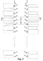
- FIG. 1 Shown in Fig. 1 is an ink jet print head 1 having a nozzle plate 2 with an array of nozzles arranged in a left column 6 and a right column 8.
- Fig. 2 shows an enlarged view of the array of nozzles in the nozzle plate 2.
- the array of nozzles includes first nozzles 10 and second nozzles 12, where the positions of the first nozzles 10 alternate with the positions of the second nozzles 12 in each of the columns 6 and 8.
- Each first nozzle 10 in the left column 6 is in horizontal alignment with a second nozzle 12 in the right column 8
- each first nozzle 10 in the right column 8 is in horizontal alignment with a second nozzle 12 in the left column 6.
- the vertical spacing between neighboring nozzles within each column is 0.042 mm ( 1 /600 inch).
- the first nozzles 10 have a diameter D 1 which is larger than the diameter D 2 of the second nozzles 12.
- the first nozzles 10 and the second nozzles 12 are also referred to as the large nozzles 10 and the small nozzles 12.
- the diameters D 1 and D 2 are determined based upon the mass of the ink droplets to be ejected from the nozzles.
- the large nozzles 10 eject ink droplets each having a mass of approximately 6 nanograms (ng) and the small nozzles 12 eject ink droplets each having a mass of approximately 2 ng.
- the invention prints pixels having eight different dot densities. Since a large and a small nozzle are in horizontal alignment at each vertical position, a large and a small droplet can be printed at a single pixel location during a single pass of the print head 1 across the paper without having to move the paper vertically with respect to the print head 1. Table 1.
- State 1 is a blank pixel, where no ink is ejected.
- State 2 the lightest printed gray-scale level, is achieved by ejecting a single 2 ng droplet at a pixel location.
- State 3 is achieved by printing two 2 ng droplets at the same pixel location, resulting in a pixel formed by 4 ng of ink.
- a first droplet is printed during a first pass of the print head 1 across the paper, and a second droplet is printed during a second pass.
- State 4 is achieved by printing a single 6 ng droplet at a pixel location.
- a state 5 pixel is formed by 8 ng of ink printed by ejecting a 2 ng droplet and a 6 ng droplet during a single pass of the print head 1.
- states 6, 7, and 8 describe pixels formed by 10, 12, and 14 ng of ink, respectively, printed during two passes of the print head 1.
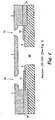
- Fig. 3 Shown in Fig. 3 are features formed on a semiconductor substrate 4 of the ink jet print head 1. As indicated in the cross-sectional view of Fig. 4, the substrate 4 is disposed below the nozzle plate 2. On the substrate are first heaters 14 and second heaters 16 consisting of rectangular patches of electrically resistive material. In the preferred embodiment of the invention, the first and second heaters 14 and 16 are formed from TaA1 thin film, which has a sheet resistance of approximately 28 ohms per square. As an electric current flows through the heaters 14 and 16, they generate heat. Ink is fed to a chamber immediately above the heaters 14 and 16 through an ink via 22. As the ink is heated by a heater 14 or 16, an ink bubble forms which expels ink through the nozzle 10 or 12.
- the second heaters 16 of the present invention are smaller in area than the first heaters 14.
- the first heaters 14 have a length L H1 and a width W H1 which, in the preferred embodiment, define an area of approximately 441 square microns.
- the second heaters 16 have an area of approximately 276 square microns defined by a length L H2 and a width W H2 .
- the first and second heaters 14 and 16 are also referred to as the large and small heaters 14 and 16.
- the large heaters 14 form larger ink bubbles than do the small heaters 16. This design is more energy-efficient than a design which uses a single heater size for both nozzle sizes.
- the large and small heaters 14 and 16 For the large and small heaters 14 and 16 to be electrically and thermodynamically compatible, they should operate at the same energy density and power density. Also, as discussed in more detail below, it is desirable to connect the large and small heaters 14 and 16 to the same voltage source.
- I 1 2 ⁇ R H ⁇ 1 A 1 ⁇ I 2 2 ⁇ R H ⁇ 2 A 2 and A 2 A 1 ⁇ I 2 2 ⁇ R H ⁇ 2 I 1 2 ⁇ R H ⁇ 1 .
- the ratio of the heater areas, A 2 /A 1 is determined by the relative energies needed to form the large and small bubbles.
- the relationship of equation (4) is satisfied by adjusting the electrical resistance R H2 of the small heaters 16 relative to the electrical resistance R H1 of the large heaters 14.
- This adjustment is made by taking advantage of the fact that: R ⁇ heater length heater width for a sheet resistor.
- R H2 may be increased by making: W H ⁇ 2 ⁇ L H ⁇ 2 while still maintaining the desired area A 2 of the small heater 16.
- W H2 is 11.75 microns and L H2 is 23.5 microns, resulting in an area A 2 of 276 square microns.
- W H1 and L H1 are 21 microns, resulting in an area A 1 of 441 square microns.
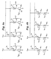
- FIG. 5a Shown in Fig. 5a is a schematic diagram of a switching circuit for selectively energizing the heaters 14 and 16 on the print head 1.
- First heater-switch pairs 17 are connected in parallel with second heater-switch pairs 19.
- Each first heater-switch pair 17 includes one of the first heaters 14 in series with a first switching device 18.
- Each second heater-switch pair 19 includes one of the second heaters 16 in series with a second switching device 20.
- the first and second switching devices 18 and 20 are MOSFET devices formed on the substrate 4.
- the heater-switch pairs 17 and 19 are connected to the same voltage source V dd .
- the device 18 When a voltage V gs of 10-12 volts is applied to a gate 24 of one of the MOSFET switching devices 18, the device 18 is enabled. When enabled, the device 18 allows a current I 1 to flow through the device 18 and the heater 14. It is the first heater's resistance R H1 to the flow of the current I 1 that generates the heat to eject the large ink droplet. Thus, when the device 18 is enabled, it acts like a closed switch through which current may flow to activate the heater 14. However, as shown in Fig. 5b, the device 18 has a finite resistance R S1 when enabled. As the current I 1 flows, a voltage drop V H1 develops across the large heater 14, and a voltage drop V S1 develops across the resistance R S1 .
- the device 20 when V gs is applied to a gate 26 of one of the MOSFET switching devices 20, the device 20 is enabled. When enabled, the device 20 allows a current I 2 to flow through the device 20 and the heater 16. Thus, when the device 20 is enabled, the heater 16 is activated. The voltage drop across the small heater 16 is V H2 . The device 20 has a finite resistance R S2 across which the voltage drop V S2 develops.
- FIGs. 5a and 5b are simplified for the purpose of illustrating the invention.
- a print head incorporating the present invention would typically also include switching devices other than those shown in Fig. 5a.
- other switching devices may be included in a logic circuit for decoding multiplexed printer signals.
- Such circuits are typically incorporated to reduce the number of I/O signal lines required to carry print signals from a printer controller to a print head.
- these other switching circuits do not significantly affect the operation of the present invention as described herein. Thus, a detailed description of such circuits is not necessary to an understanding of the present invention.
- ink jet print head design One goal in ink jet print head design is to minimize heater-to-heater power variations. So that the size of the ink bubbles produced by same-sized heaters is consistent across the array, each large heater 14 should dissipate the same power as every other large heater 14, and each small heater 16 should dissipate the same power as every other small heater 16. If same-sized heaters dissipate differing amounts of power in generating heat to produce ink bubbles, undesirable variations in ink droplet size occur. Such variations in ink droplet size result in degraded print quality.
- the present invention minimizes variations in dissipated power from heater to heater by approximately equalizing the voltage drops across all of the heaters 14 and 16, both large and small. Since the heater-switch pairs 17 and 19 are connected in parallel, equalizing the voltage drops across the heaters 14 and 16 requires equalizing the voltage drops across the switching devices 18 and 20.
- the resistance of a MOSFET device is the sum of its source resistance, drain resistance, and channel resistance.
- the source and drain resistances of a MOSFET device are determined, at least in part, by the source-drain line widths of the device.
- the preferred embodiment of the invention achieves the relationship of equation (9) by adjusting the source-drain line widths of the first and second switching devices 18 and 20.
- the first switching device 18 includes a source region 28 separated from a drain region 30 by a channel 32 having a width C.
- the source-drain line width of the first switching device 18 is represented by W L1 and the channel length of the first switching device 18 is represented by L S1 .
- the second switching device 20 includes a source region 34 separated from a drain region 36 by the channel 32.
- the source-drain line width and the channel length of the second switching device 20 is represented by W L2 and L S2 , respectively.
- adjacent nozzles and heaters are vertically spaced by 0.042 mm ( 1 /600 inch).
- the total width that an adjacent pair of switching devices 18 and 20 may occupy is 2 /600 inch or approximately 84.7 ⁇ m.
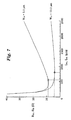
- Fig. 7 shows a summary solution for a first order simulation of the preferred MOSFET devices 18 and 20 which meets the requirements of equations (9) and (13).
- the preferred values for W L1 and W L2 are 13.1 and 3.1 ⁇ m, respectively.
- a minimum value of R S1 , 4.3 ⁇ results when L S1 equals approximately 800 ⁇ m. If R S1 equals 4.3 ⁇ , the relationship of equation (9) is satisfied when R S2 equals 8.6 ⁇ . With continued reference to Fig. 7, when R S2 equals 8.6 ⁇ , L S2 equals approximately 570 ⁇ m.
- W S1 and W S2 are approximately 62.3 ⁇ m and 22.4 ⁇ m, respectively. Therefore, the dimensional values for a preferred embodiment of the switching devices 18 and 20 are summarized as follows: W L1 ⁇ 13.1 ⁇ m, W L2 ⁇ 3.1 ⁇ m, W S1 ⁇ 62.3 ⁇ m, W S2 ⁇ 22.4 ⁇ m, L S1 ⁇ 800 ⁇ m, L S2 ⁇ 570 ⁇ m, and C ⁇ 2.5 ⁇ m.
- first and second voltage sources V dd1 and V dd2 , are provided to drive the first and second heater-switch pairs 17 and 19.
- the first heater-switch pairs 17 are connected in parallel across the first voltage source V dd1
- the second heater-switch pairs 19 are connected in parallel across the second voltage source V dd2 .
- the heat energy generated by the heaters 14 and 16 may be tailored to the ink droplet size by adjusting the voltage V dd1 relative to the voltage V dd2 , rather than by adjusting the resistance R H1 relative to R H2 .
- the voltage V dd2 is less than the voltage V dd1 , such that the second heaters 16 generate less heat energy when activated than do the first heaters 14.
- the areas of the heaters 14 and 16 in the second embodiment are preferably maintained at 441 and 276 square microns, respectively. As discussed above, this provides for the most efficient energy transfer for generating ink droplets of two different sizes.
- W H1 and L H1 are approximately 21 microns.
- W H2 and L H2 are preferably about 16.6 microns.
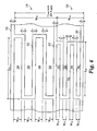
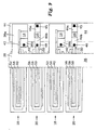
- a first metal bus 38 which is connected to the voltage source V dd1 , preferably resides at the same chip layer as the heaters 14 and 16.
- the bus 38 is connected to metal traces 38a which supply the voltage V dd1 to one side of the large heaters 14.
- the other sides of the large heaters 14 are connected to metal traces 38b in the same layer.
- the metal traces 38b are connected, by way of vias 40, to drains 42 of the first switching devices 18 which reside in a layer below the large heaters 14.
- a second metal bus 44 is connected to the voltage source V dd2 .
- the bus 44 preferably resides at a chip layer below the layer containing the heaters 14 and 16, such as the layer containing the switching devices 18 and 20.
- the bus 44 is connected, by way of vias 45, to metal traces 46a residing at the same layer as the heaters 14 and 16.
- the traces 46a are connected to one side of the small heaters 16.
- the voltage V dd2 is supplied to one side of the small heaters 16 by way of the bus 44, the vias 45, and the traces 46a.
- Metal traces 46b also residing in the same layer as the heaters 14 and 16, are connected to the other side of the small heaters 16.
- the metal traces 46b are connected, by way of vias 48, to drains 50 of the second switching devices 20, which preferably reside in the same layer as the first switching devices 18. Also, shown in Fig. 9 are sources 52 and gates 54 of the first switching devices 18, and sources 56 and gates 58 of the second switching devices 20.
- Fig. 9 provides the two separate voltage rails V dd1 and V dd2 to the vertically alternating large and small heaters 14 and 16.
- Fig. 9 depicts an exemplary portion of the heater wiring geometry, and it will be appreciated that the pattern shown in Fig. 9 repeats in the vertical dimension to form the rest of the heater array.
Landscapes
- Particle Formation And Scattering Control In Inkjet Printers (AREA)
- Ink Jet (AREA)
Claims (9)
- Tintenstrahldruckkopf (1) mit einer Mehrzahl von Düsen (6, 8), durch die Tröpfchen von Tinte in Richtung auf ein Druckmedium ausgeschleudert werden, wobei die Mehrzahl von Düsen erste Düsen (10) mit einem ersten Durchmesser (D1) zum Ausschleudern von Tröpfchen von Tinte mit einer ersten Masse und zweite Düsen (12) mit einem zweiten Durchmesser (D2) zum Ausschleudern von Tröpfchen von Tinte mit einer zweiten Masse umfasst, wobei der erste Durchmesser größer als der zweite Durchmesser ist und die erste Masse größer als die zweite Masse ist, wobei der Druckkopf umfasst:eine Düsenplatte (2), die die Mehrzahl von Düsen enthält;ein Substrat (4), das benachbart zur Düsenplatte angeordnet ist;erste Heizer (14), die auf dem Substrat benachbart zu den ersten Düsen angeordnet sind, wobei jeder der ersten Heizer einer entsprechenden ersten Düse zugeordnet ist, wobei jeder der ersten Heizer elektrisch widerstandsbehaftetes Material umfasst und einen ersten elektrischen Heizerwiderstand aufweist, wobei jeder der ersten Heizer Wärme erzeugt, während ein erster elektrischer Strom im Wesentlichen in einer ersten Richtung durch das elektrisch widerstandsbehaftete Material fließt;erste Schaltbauelemente (18), die auf dem Substrat benachbart zu den ersten Heizern angeordnet sind, wobei jedes der ersten Schaltbauelemente mit einem entsprechenden ersten Heizer elektrisch hintereinandergeschaltet ist, wobei die ersten Schaltbauelemente jeweils einen ersten elektrischen Schaltwiderstand aufweisen;zweite Heizer (16), die auf dem Substrat benachbart zu den zweiten Düsen angeordnet sind, wobei jeder der zweiten Heizer einer entsprechenden zweiten Düse zugeordnet ist, wobei jeder der zweiten Heizer elektrisch widerstandsbehaftetes Material umfasst und einen zweiten elektrischen Heizerwiderstand aufweist, wobei jeder der zweiten Heizer Wärme erzeugt, während ein zweiter elektrischer Strom im Wesentlichen in der ersten Richtung durch das elektrisch widerstandsbehaftete Material fließt; undzweite Schaltbauelemente (20), die auf dem Substrat benachbart zu den zweiten Heizern angeordnet sind, wobei jedes der zweiten Schaltbauelemente mit einem entsprechenden zweiten Heizer elektrisch hintereinandergeschaltet ist, wobei die zweiten Schaltbauelemente jeweils einen zweiten elektrischen Schaltwiderstand aufweisen,dadurch gekennzeichnet, dass der zweite elektrische Schaltwiderstand größer als der erste elektrische Schaltwiderstand ist.
- Druckkopf nach Anspruch 1, bei dem der erste Heizerwiderstand kleiner als der zweite Heizerwiderstand ist.
- Druckkopf nach Anspruch 1 oder 2, weiter umfassend:die ersten Heizer, die jeweils einen ersten Heizerbereich auf dem Substrat einnehmen, der durch eine erste Heizerlänge (LH1) in der ersten Richtung und eine erste Heizerbreite (WH1) in einer zweiten Richtung festgelegt ist, die zur ersten Richtung orthogonal ist, unddie zweiten Heizer, die jeweils einen zweiten Heizerbereich auf dem Substrat einnehmen, der durch eine zweite Heizerlänge (LH2) in der ersten Richtung und eine zweite Heizerbreite (WH2) in der zweiten Richtung festgelegt ist,wobei die zweite Heizerbreite kleiner als die erste Heizerbreite ist.
- Druckkopf nach Anspruch 1 oder 2, weiter umfassend:die ersten Heizer, die jeweils einen ersten Heizerbereich auf dem Substrat einnehmen, der durch eine erste Heizerlänge (LH1) in der ersten Richtung und eine erste Heizerbreite (WH1) in einer zweiten Richtung festgelegt ist, die zur ersten Richtung orthogonal ist, unddie zweiten Heizer, die jeweils einen zweiten Heizerbereich auf dem Substrat einnehmen, der durch eine zweite Heizerlänge (LH2) in der ersten Richtung und eine zweite Heizerbreite (WH2) in der zweiten Richtung festgelegt ist,wobei die zweite Heizerlänge größer als die erste Heizerlänge ist.
- Druckkopf nach einem vorangehenden Anspruch, weiter umfassend:die ersten Heizer, die jeweils einen ersten Heizerbereich auf dem Substrat einnehmen; unddie zweiten Heizer, die jeweils einen zweiten Heizerbereich auf dem Substrat einnehmen,wobei der zweite Heizerbereich kleiner als der erste Heizerbereich ist.
- Druckkopf nach einem vorangehenden Anspruch, weiter umfassend:die ersten Schaltbauelemente, die jeweils einen ersten Schaltbereich auf dem Substrat einnehmen, wobei der erste Schaltbereich durch eine erste Schaltlänge (LS1) in der ersten Richtung und eine erste Schaltbreite (WS1) in einer zweiten Richtung festgelegt ist, die zur ersten Richtung orthogonal ist, unddie zweiten Schaltbauelemente, die jeweils einen zweiten Schaltbereich auf dem Substrat einnehmen, wobei der zweite Schaltbereich durch eine zweite Schaltlänge (LS2) in der ersten Richtung und eine zweite Schaltbreite (WS2) in der zweiten Richtung festgelegt ist,wobei die erste Schaltbreite größer als die zweite Schaltbreite ist.
- Druckkopf nach einem der Ansprüche 1 bis 5, weiter umfassend:die ersten Schaltbauelemente, die jeweils einen ersten Schaltbereich auf dem Substrat einnehmen, wobei der erste Schaltbereich durch eine erste Schaltlänge (LS1) in der ersten Richtung und eine erste Schaltbreite (WS1) in einer zweiten Richtung festgelegt ist, die zur ersten Richtung orthogonal ist, unddie zweiten Schaltbauelemente, die jeweils einen zweiten Schaltbereich auf dem Substrat einnehmen, wobei der zweite Schaltbereich durch eine zweite Schaltlänge (LS2) in der ersten Richtung und eine zweite Schaltbreite (WS2) in der zweiten Richtung festgelegt ist,wobei die erste Schaltlänge größer als die zweite Schaltlänge ist.
- Druckkopf nach einem vorangehenden Anspruch, weiter umfassend:die ersten Schaltbauelemente, die jeweils einen ersten Schaltbereich auf dem Substrat einnehmen, unddie zweiten Schaltbauelemente, die jeweils einen zweiten Schaltbereich auf dem Substrat einnehmen,wobei der erste Schaltbereich größer als der zweite Schaltbereich ist.
- Druckkopf nach einem vorangehenden Anspruch, weiter umfassend:die ersten Schaltbauelemente, die in ersten Positionen angeordnet sind, die in der zweiten Richtung ausgerichtet sind; unddie zweiten Schaltbauelemente, die in zweiten Positionen angeordnet sind, die in der zweiten Richtung ausgerichtet sind,wobei die ersten Positionen mit den zweiten Positionen alternieren.
Priority Applications (1)
| Application Number | Priority Date | Filing Date | Title |
|---|---|---|---|
| EP07020253A EP1886824A1 (de) | 1999-08-27 | 2000-08-24 | Druckkopf mit doppelter Tröpfchengröße |
Applications Claiming Priority (3)
| Application Number | Priority Date | Filing Date | Title |
|---|---|---|---|
| US09/384,803 US6137502A (en) | 1999-08-27 | 1999-08-27 | Dual droplet size printhead |
| US384803 | 1999-08-27 | ||
| EP00959364A EP1214199B1 (de) | 1999-08-27 | 2000-08-24 | Druckkopf mit zwei tröpfchengrössen |
Related Parent Applications (1)
| Application Number | Title | Priority Date | Filing Date |
|---|---|---|---|
| EP00959364A Division EP1214199B1 (de) | 1999-08-27 | 2000-08-24 | Druckkopf mit zwei tröpfchengrössen |
Related Child Applications (1)
| Application Number | Title | Priority Date | Filing Date |
|---|---|---|---|
| EP07020253A Division EP1886824A1 (de) | 1999-08-27 | 2000-08-24 | Druckkopf mit doppelter Tröpfchengröße |
Publications (3)
| Publication Number | Publication Date |
|---|---|
| EP1520712A2 EP1520712A2 (de) | 2005-04-06 |
| EP1520712A3 EP1520712A3 (de) | 2005-07-13 |
| EP1520712B1 true EP1520712B1 (de) | 2007-12-05 |
Family
ID=23518820
Family Applications (3)
| Application Number | Title | Priority Date | Filing Date |
|---|---|---|---|
| EP00959364A Expired - Lifetime EP1214199B1 (de) | 1999-08-27 | 2000-08-24 | Druckkopf mit zwei tröpfchengrössen |
| EP07020253A Withdrawn EP1886824A1 (de) | 1999-08-27 | 2000-08-24 | Druckkopf mit doppelter Tröpfchengröße |
| EP04024987A Expired - Lifetime EP1520712B1 (de) | 1999-08-27 | 2000-08-24 | Druckkopf mit zwei tröpfchengrössen |
Family Applications Before (2)
| Application Number | Title | Priority Date | Filing Date |
|---|---|---|---|
| EP00959364A Expired - Lifetime EP1214199B1 (de) | 1999-08-27 | 2000-08-24 | Druckkopf mit zwei tröpfchengrössen |
| EP07020253A Withdrawn EP1886824A1 (de) | 1999-08-27 | 2000-08-24 | Druckkopf mit doppelter Tröpfchengröße |
Country Status (9)
| Country | Link |
|---|---|
| US (1) | US6137502A (de) |
| EP (3) | EP1214199B1 (de) |
| JP (2) | JP4041914B2 (de) |
| KR (1) | KR100743989B1 (de) |
| CN (1) | CN1192895C (de) |
| AU (1) | AU7070000A (de) |
| DE (2) | DE60035280T2 (de) |
| MX (1) | MXPA02001967A (de) |
| WO (1) | WO2001015904A1 (de) |
Families Citing this family (36)
| Publication number | Priority date | Publication date | Assignee | Title |
|---|---|---|---|---|
| US6422676B1 (en) * | 2001-06-19 | 2002-07-23 | Hewlett-Packard Company | Compact ink jet printhead |
| JP3871320B2 (ja) * | 2001-06-21 | 2007-01-24 | キヤノン株式会社 | インクジェット記録ヘッド |
| JP3848218B2 (ja) * | 2001-06-21 | 2006-11-22 | キヤノン株式会社 | インクジェット記録ヘッド |
| US6966629B2 (en) * | 2002-07-18 | 2005-11-22 | Canon Kabushiki Kaisha | Inkjet printhead, driving method of inkjet printhead, and substrate for inkjet printhead |
| US6808241B2 (en) * | 2003-03-11 | 2004-10-26 | Hewlett-Packard Development Company, L.P. | Fluid ejection device |
| US6761435B1 (en) * | 2003-03-25 | 2004-07-13 | Lexmark International, Inc. | Inkjet printhead having bubble chamber and heater offset from nozzle |
| US6883889B2 (en) * | 2003-04-30 | 2005-04-26 | Hewlett-Packard Development Company, L.P. | Fluid ejection device |
| US7108352B2 (en) * | 2003-05-16 | 2006-09-19 | Canon Kabushiki Kaisha | Liquid-jet recording head |
| JP4115465B2 (ja) * | 2004-06-02 | 2008-07-09 | キヤノン株式会社 | インクジェット記録ヘッド、インクジェット記録ヘッドを備えるインクジェットカートリッジ、及びインクジェット記録装置 |
| US7198353B2 (en) * | 2004-06-30 | 2007-04-03 | Lexmark International, Inc. | Integrated black and colored ink printheads |
| JP4533055B2 (ja) * | 2004-09-07 | 2010-08-25 | キヤノン株式会社 | 液体噴射記録ヘッド |
| JP2006076011A (ja) * | 2004-09-07 | 2006-03-23 | Canon Inc | 液体噴射記録ヘッド |
| US7258410B2 (en) * | 2004-11-10 | 2007-08-21 | Xerox Corporation | Method and apparatus for reducing intercolor bleed to improve print quality |
| JP4614388B2 (ja) * | 2005-04-01 | 2011-01-19 | キヤノン株式会社 | 記録装置、記録ヘッド及びその駆動方法 |
| US7588305B2 (en) * | 2005-05-31 | 2009-09-15 | Xerox Corporation | Dual drop printing mode using full length waveforms to achieve head drop mass differences |
| JP4298697B2 (ja) * | 2005-11-25 | 2009-07-22 | キヤノン株式会社 | インクジェット記録ヘッド、インクジェット記録ヘッドを備えるインクジェットカートリッジ、及びインクジェット記録装置 |
| US20070176982A1 (en) * | 2006-02-01 | 2007-08-02 | Lexmark International, Inc. | Inkjet actuator substrate having at least one non-uniform ink via |
| US7909428B2 (en) * | 2006-07-28 | 2011-03-22 | Hewlett-Packard Development Company, L.P. | Fluid ejection devices and methods of fabrication |
| US7918366B2 (en) * | 2006-09-12 | 2011-04-05 | Hewlett-Packard Development Company, L.P. | Multiple drop weight printhead and methods of fabrication and use |
| EP2099869B1 (de) | 2006-10-31 | 2013-05-01 | Sensient Colors Inc. | Modifizierte pigmente, deren herstellung und verwendung |
| US7905577B2 (en) * | 2006-12-15 | 2011-03-15 | Canon Kabushiki Kaisha | Printhead substrate having electrothermal transducers arranged at high density, printhead, and printing apparatus |
| JP4926691B2 (ja) * | 2006-12-21 | 2012-05-09 | キヤノン株式会社 | インクジェット記録ヘッド、およびインクジェット記録ヘッドの製造方法 |
| JP5197178B2 (ja) * | 2007-06-27 | 2013-05-15 | キヤノン株式会社 | インクジェット記録ヘッド用基板およびインクジェット記録ヘッド |
| JP5043539B2 (ja) * | 2007-07-02 | 2012-10-10 | キヤノン株式会社 | 液体噴射記録ヘッドの製造方法 |
| JP5706159B2 (ja) | 2007-08-23 | 2015-04-22 | センシエント カラーズ エルエルシー | 自己分散型顔料ならびにその製造方法および使用 |
| JP5046855B2 (ja) * | 2007-10-24 | 2012-10-10 | キヤノン株式会社 | 素子基板、記録ヘッド、ヘッドカートリッジ及び記録装置 |
| US8231195B2 (en) * | 2008-05-08 | 2012-07-31 | Canon Kabushiki Kaisha | Print element substrate, printhead, and printing apparatus |
| US8167411B2 (en) * | 2008-05-08 | 2012-05-01 | Canon Kabushiki Kaisha | Print element substrate, inkjet printhead, and printing apparatus |
| ATE547249T1 (de) * | 2008-05-08 | 2012-03-15 | Canon Kk | Druckelementsubstrat, druckkopf und druckvorrichtung |
| KR20110135989A (ko) | 2009-04-07 | 2011-12-20 | 센션트 컬러스 엘엘씨 | 자가-분산 입자 및 그의 제조 및 사용 방법 |
| JP5634090B2 (ja) * | 2010-03-24 | 2014-12-03 | キヤノン株式会社 | 液体吐出ヘッド |
| IT201700013746A1 (it) | 2017-02-08 | 2018-08-08 | Tecnaria S P A | Dispositivo per la giunzione meccanica di barre di acciaio |
| JP7389961B2 (ja) * | 2019-07-26 | 2023-12-01 | 株式会社リコー | 液体吐出ヘッド、液体吐出ユニット、及び、液体を吐出する装置 |
| DE102020000642A1 (de) * | 2019-12-17 | 2021-06-17 | Mahle International Gmbh | Elektrische Heizeinrichtung und Verfahren zum Betreiben der elektrischen Heizeinrichtung |
| WO2022053257A1 (en) * | 2020-09-09 | 2022-03-17 | Memjet Technology Limited | Method and print chip for single-pass monochrome printing at high speeds |
| US11642887B2 (en) | 2021-04-22 | 2023-05-09 | Funai Electric Co., Ltd. | Ejection head having optimized fluid ejection characteristics |
Family Cites Families (21)
| Publication number | Priority date | Publication date | Assignee | Title |
|---|---|---|---|---|
| US4746935A (en) * | 1985-11-22 | 1988-05-24 | Hewlett-Packard Company | Multitone ink jet printer and method of operation |
| US4719477A (en) * | 1986-01-17 | 1988-01-12 | Hewlett-Packard Company | Integrated thermal ink jet printhead and method of manufacture |
| US5030971B1 (en) * | 1989-11-29 | 2000-11-28 | Xerox Corp | Precisely aligned mono- or multi-color roofshooter type printhead |
| US5075250A (en) * | 1991-01-02 | 1991-12-24 | Xerox Corporation | Method of fabricating a monolithic integrated circuit chip for a thermal ink jet printhead |
| US5122812A (en) * | 1991-01-03 | 1992-06-16 | Hewlett-Packard Company | Thermal inkjet printhead having driver circuitry thereon and method for making the same |
| US5159353A (en) * | 1991-07-02 | 1992-10-27 | Hewlett-Packard Company | Thermal inkjet printhead structure and method for making the same |
| US5208605A (en) * | 1991-10-03 | 1993-05-04 | Xerox Corporation | Multi-resolution roofshooter printheads |
| DE69316432T2 (de) * | 1992-04-28 | 1998-05-07 | Hewlett Packard Co | Optimierung der Druckqualität und Zuverlässigkeit bei einem CYMK-Drucksystem |
| JPH06151532A (ja) * | 1992-11-13 | 1994-05-31 | Tokyo Electron Yamanashi Kk | プローブ装置 |
| US5412410A (en) * | 1993-01-04 | 1995-05-02 | Xerox Corporation | Ink jet printhead for continuous tone and text printing |
| US5357081A (en) * | 1993-01-21 | 1994-10-18 | Hewlett-Packard Company | Power supply for individual control of power delivered to integrated drive thermal inkjet printhead heater resistors |
| ATE152399T1 (de) * | 1993-02-26 | 1997-05-15 | Canon Kk | Tintenstrahldruckkopf, tintenstrahlkopf-kartusche und druckgerät |
| US5519417A (en) * | 1994-03-31 | 1996-05-21 | Xerox Corporation | Power control system for a printer |
| US5635968A (en) * | 1994-04-29 | 1997-06-03 | Hewlett-Packard Company | Thermal inkjet printer printhead with offset heater resistors |
| JPH08332727A (ja) * | 1995-06-06 | 1996-12-17 | Canon Inc | インクジェット記録ヘッド及びインクジェット記録装置 |
| US5745131A (en) * | 1995-08-03 | 1998-04-28 | Xerox Corporation | Gray scale ink jet printer |
| US6447088B2 (en) * | 1996-01-16 | 2002-09-10 | Canon Kabushiki Kaisha | Ink-jet head, an ink-jet-head cartridge, an ink-jet apparatus and an ink-jet recording method used in gradation recording |
| JPH09286108A (ja) * | 1996-04-22 | 1997-11-04 | Canon Inc | インクジェットプリントヘッドの基体、インクジェットプリントヘッド、およびインクジェットプリント装置 |
| JPH10166576A (ja) * | 1996-12-12 | 1998-06-23 | Minolta Co Ltd | インクジェット記録ヘッドおよびインクジェット記録装置 |
| US6234612B1 (en) * | 1997-03-25 | 2001-05-22 | Lexmark International, Inc. | Ink jet printing apparatus having first and second print cartridges receiving energy pulses from a common drive circuit |
| US6102528A (en) * | 1997-10-17 | 2000-08-15 | Xerox Corporation | Drive transistor for an ink jet printhead |
-
1999
- 1999-08-27 US US09/384,803 patent/US6137502A/en not_active Expired - Lifetime
-
2000
- 2000-08-24 EP EP00959364A patent/EP1214199B1/de not_active Expired - Lifetime
- 2000-08-24 WO PCT/US2000/023279 patent/WO2001015904A1/en not_active Ceased
- 2000-08-24 KR KR1020027002453A patent/KR100743989B1/ko not_active Expired - Fee Related
- 2000-08-24 JP JP2001520296A patent/JP4041914B2/ja not_active Expired - Fee Related
- 2000-08-24 MX MXPA02001967A patent/MXPA02001967A/es active IP Right Grant
- 2000-08-24 DE DE60035280T patent/DE60035280T2/de not_active Expired - Fee Related
- 2000-08-24 CN CNB00813250XA patent/CN1192895C/zh not_active Expired - Fee Related
- 2000-08-24 DE DE60037348T patent/DE60037348T2/de not_active Expired - Fee Related
- 2000-08-24 EP EP07020253A patent/EP1886824A1/de not_active Withdrawn
- 2000-08-24 EP EP04024987A patent/EP1520712B1/de not_active Expired - Lifetime
- 2000-08-24 AU AU70700/00A patent/AU7070000A/en not_active Abandoned
-
2006
- 2006-07-24 JP JP2006201330A patent/JP2006327208A/ja active Pending
Also Published As
| Publication number | Publication date |
|---|---|
| CN1192895C (zh) | 2005-03-16 |
| EP1214199B1 (de) | 2007-06-20 |
| HK1048969A1 (en) | 2003-04-25 |
| KR20020067494A (ko) | 2002-08-22 |
| WO2001015904A1 (en) | 2001-03-08 |
| EP1214199A1 (de) | 2002-06-19 |
| JP2003508257A (ja) | 2003-03-04 |
| DE60035280T2 (de) | 2008-02-21 |
| CN1376114A (zh) | 2002-10-23 |
| JP4041914B2 (ja) | 2008-02-06 |
| EP1214199A4 (de) | 2003-04-02 |
| DE60037348T2 (de) | 2008-10-23 |
| DE60037348D1 (de) | 2008-01-17 |
| US6137502A (en) | 2000-10-24 |
| MXPA02001967A (es) | 2002-10-31 |
| JP2006327208A (ja) | 2006-12-07 |
| DE60035280D1 (de) | 2007-08-02 |
| AU7070000A (en) | 2001-03-26 |
| EP1520712A3 (de) | 2005-07-13 |
| KR100743989B1 (ko) | 2007-08-01 |
| EP1520712A2 (de) | 2005-04-06 |
| EP1886824A1 (de) | 2008-02-13 |
Similar Documents
| Publication | Publication Date | Title |
|---|---|---|
| EP1520712B1 (de) | Druckkopf mit zwei tröpfchengrössen | |
| US6478404B2 (en) | Ink jet printhead | |
| EP1309451B1 (de) | Energetisch ausgeglichener entwurf eines tintenstrahldruckkopfes | |
| US6523935B2 (en) | Narrow ink jet printhead | |
| AU2001290647A1 (en) | Narrow multi-color ink jet printhead | |
| AU2001290665A1 (en) | Energy balanced printhead design | |
| AU2001288890A1 (en) | Narrow ink jet printhead | |
| US6422676B1 (en) | Compact ink jet printhead | |
| DE60110230T2 (de) | Tintenstrahldruckkopf mit ausgeglichenem energieumsatz an widerstandselementen durch angepasste fet-schaltkreise | |
| HK1048969B (en) | Dual droplet size printead |
Legal Events
| Date | Code | Title | Description |
|---|---|---|---|
| PUAI | Public reference made under article 153(3) epc to a published international application that has entered the european phase |
Free format text: ORIGINAL CODE: 0009012 |
|
| AC | Divisional application: reference to earlier application |
Ref document number: 1214199 Country of ref document: EP Kind code of ref document: P |
|
| AK | Designated contracting states |
Kind code of ref document: A2 Designated state(s): DE FR GB |
|
| PUAL | Search report despatched |
Free format text: ORIGINAL CODE: 0009013 |
|
| AK | Designated contracting states |
Kind code of ref document: A3 Designated state(s): DE FR GB |
|
| 17P | Request for examination filed |
Effective date: 20060113 |
|
| AKX | Designation fees paid |
Designated state(s): DE FR GB |
|
| 17Q | First examination report despatched |
Effective date: 20060823 |
|
| GRAP | Despatch of communication of intention to grant a patent |
Free format text: ORIGINAL CODE: EPIDOSNIGR1 |
|
| GRAS | Grant fee paid |
Free format text: ORIGINAL CODE: EPIDOSNIGR3 |
|
| GRAA | (expected) grant |
Free format text: ORIGINAL CODE: 0009210 |
|
| AC | Divisional application: reference to earlier application |
Ref document number: 1214199 Country of ref document: EP Kind code of ref document: P |
|
| AK | Designated contracting states |
Kind code of ref document: B1 Designated state(s): DE FR GB |
|
| REG | Reference to a national code |
Ref country code: GB Ref legal event code: FG4D |
|
| REF | Corresponds to: |
Ref document number: 60037348 Country of ref document: DE Date of ref document: 20080117 Kind code of ref document: P |
|
| ET | Fr: translation filed | ||
| PLBE | No opposition filed within time limit |
Free format text: ORIGINAL CODE: 0009261 |
|
| STAA | Information on the status of an ep patent application or granted ep patent |
Free format text: STATUS: NO OPPOSITION FILED WITHIN TIME LIMIT |
|
| 26N | No opposition filed |
Effective date: 20080908 |
|
| GBPC | Gb: european patent ceased through non-payment of renewal fee |
Effective date: 20080824 |
|
| REG | Reference to a national code |
Ref country code: FR Ref legal event code: ST Effective date: 20090430 |
|
| PG25 | Lapsed in a contracting state [announced via postgrant information from national office to epo] |
Ref country code: FR Free format text: LAPSE BECAUSE OF NON-PAYMENT OF DUE FEES Effective date: 20080901 Ref country code: DE Free format text: LAPSE BECAUSE OF NON-PAYMENT OF DUE FEES Effective date: 20090303 |
|
| PG25 | Lapsed in a contracting state [announced via postgrant information from national office to epo] |
Ref country code: GB Free format text: LAPSE BECAUSE OF NON-PAYMENT OF DUE FEES Effective date: 20080824 |