BACKGROUND OF THE INVENTION
The present invention relates to a
radiological imaging system using a radiation and
particularly relates to a radiological imaging system
suitable for carrying out two or more kinds of
radiological examinations including an X-ray CT
examination and a positron emission computed tomography
(hereinafter referred to as "PET") examination.
Examination techniques using radiations
realize nondestructive examinations in the body of an
examinee. Particularly radiological examination
techniques for a human body include X-ray CT, PET,
single photon emission computed tomography (hereinafter
referred to as "SPECT").
In all of these techniques, a physical
quantity to be examined is measured as an integral
value of the flying direction of a radiation and the
integral value is inversely projected, so that a
physical quantity of each voxel in the body of an
examinee is calculated and an image is created. In
these techniques, it is necessary to process an
enormous amount of data and extremely fine images can
be provided at high speed due to the rapid development
of computer technology in recent years.
The X-ray CT technique measures the intensity
of X-rays having passed through an examinee and images
the morphological information of the examinee according
to a rate of X-rays passing through the body. X-rays
are radiated from an X-ray source to the examinee, the
intensity of X-rays having passed through the body is
measured by a detection element disposed on the other
side of the examinee, and the distribution of
integrated absorption coefficients of the examinee is
measured. Based on the integrated absorption
coefficients, an absorption coefficient of each voxel
is determined using filtered back projection method
described in IEEE Transactions on Nuclear Science, NS-21
vol., page 21, and the value is converted into a CT
value. A source of about 80 keV is frequently used for
X-ray CT.
Meanwhile, PET and SPECT are methods capable
of detecting a function and metabolism at a molecular
biological level where detection cannot be performed by
X-ray CT, thereby providing a functional image of a
body. In PET, radioactive chemicals labeled positron
emitting nuclides such as 18F, 15O, and 11C are
administered, and the distribution is measured and
imaged. The chemicals include fluorodeoxyglucose (2-[F-18]fluoro-2-deoxy-D-glucose,
18FDG), which highly
accumulates on a tumor tissue according to glucose
metabolism and is used to identify a tumor region.
A radionuclide taken in the body decays and
emits a positron (β+). The emitted positron releases a
pair of annihilated γ-rays having an energy of 511 keV
when being bound with electrons and annihilated. Since
the pair of annihilated γ-rays are radiated
substantially in opposite directions (180° ± 0.6°), the
pair of annihilated γ-rays are simultaneously detected
by detector elements which are arranged so as to
surround the examinee, and radiating direction data is
accumulated to obtain projection data. By inversely
projecting the projection data (using the filtered back
projection method), the emitting position (position
where the radionuclide accumulates) can be identified
and imaged.
In SPECT, radioactive chemicals labeled
single photon emitting nuclides are administered and
the distribution is measured and imaged. A single γ-ray
with an energy of about 100 keV is radiated from the
chemicals, and the single γ-ray is measured by the
detection element. Since the flying direction cannot
be identified in the measurement of the single γ-ray, a
collimator is inserted at the front of the detection
element and only γ-rays in a specific direction are
detected, so that projection data is obtained in SPECT.
As in the case of PET, projection data is inversely
projected by using the filtered back projection method,
etc., so that image data is obtained. SPECT is
different from PET in that coincidence detection is not
necessary due to single γ-ray measurement and the number
of detection elements is small. Thus, the
configuration of the apparatus is simple with
relatively low cost. On the other hand, since SPECT
uses a collimator, the detection rate of γ-rays is low
and picture quality is poor in ordinary cases.
As described above, in PET and SPECT, a
functional image is obtained using body metabolism.
Thus, although a part where chemicals accumulate can be
extracted with high contrast, the positional
relationship of surrounding organs cannot be
understood. For this reason, attention is being given
to techniques for combining a morphological image of X-ray
CT and a functional image of PET and SPECT to
conduct a higher level of diagnosis (refer to JP-A-7-20245
(paragraph No. 0010, Fig. 1)).
In a radiological imaging system where a
morphological image of conventional X-ray CT and a
functional image of PET and SPECT are combined, a
scintillator is used as a γ-ray detector to obtain a
functional image of PET, SPECT and so on. The
scintillator temporarily transforms a received γ-ray
into visible light and then transforms the light into
an electric signal by using a photomultiplier tube
(photomultiplier). The scintillator has a low
resolution of energy because the number of generated
photons is small in the transformation into visible
light and the two steps of transformation are necessary
as described above. Thus, it is not always possible to
conduct an accurate diagnosis. Particularly a
quantitative evaluation cannot be made in 3D imaging of
PET due to a reduction in energy resolution. This is
because a γ-ray energy threshold value has to be reduced
due to a low energy resolution and internal scattering,
which is noise increased in 3D imaging, is frequently
detected. Therefore, a PET apparatus of a scintillator
system generally comprises a 2D imaging function to
conduct a highly quantitative examination. In the 2D
imaging, septa are inserted in the scintillator to
prevent the entry of γ-rays from a part other than a 2D
region.
Further, absorption correction is necessary
to obtain an image with higher accuracy in a PET
examination. γ-rays from a deep portion of the body are
prone to be absorbed in the body as compared with a
body surface. High picture quality and high
quantitativeness can be achieved by correcting an
amount of absorbed γ-rays in the body (absorption
correction). In a PET apparatus of a single gantry
system, when absorption correction is performed, it is
necessary to hold a source and carry out measurement
while rotating the source in the scintillator.
Therefore, in the PET apparatus of the
scintillator system, the gantry has a large size due to
the photomultiplier, septa, and the source for
absorption correction. Moreover, in the case of a
radiological imaging system having a conventional
serial arrangement of X-ray CT, PET, SPECT, etc., the
overall apparatus is prone to increase in size, thereby
intimidating an examinee. Such a problem has to be
solved.
An object of the present invention is to
provide a radiological imaging system which can improve
an energy resolution and achieve an accurate diagnosis.
SUMMARY OF THE INVENTION
In order to solve the problem, in a first
invention, semiconductor radiation detectors are used
for a first imaging apparatus (PET imaging apparatus)
to increase detection accuracy. In this configuration,
the semiconductor radiation detectors are used to
directly detect a radiation, thereby improving a
position resolution and an energy resolution. Further,
since an energy resolution can be improved, internal
scattering is removed (noise is reduced). Therefore,
it is possible to improve quantitativeness in 3D
imaging and eliminate the need for the septa for 2D
imaging, thereby miniaturizing the apparatus. Further,
detection elements can be smaller in size, achieving a
radiological imaging system which is entirely
miniaturized.
Besides, since absorption correction can be
performed using a second imaging apparatus (X-ray CT
imaging apparatus), it is not necessary to provide an
absorption correction source (γ-ray, etc.) in the first
imaging apparatus, thereby further miniaturizing the
apparatus.
In a second invention, a semiconductor
radiation detector is used as a radiation detector of
the second imaging apparatus (X-ray CT imaging
apparatus). In this configuration, the detection
elements can be smaller in size, achieving a
radiological imaging system which is entirely
miniaturized.
In a third invention, the first imaging
apparatus (PET imaging apparatus) is formed with a
smaller size than the second imaging apparatus (X-ray
CT imaging apparatus), and the first imaging apparatus
is disposed in front of the second imaging apparatus.
Thus, the overall apparatus becomes less intimidating
to an examinee.
The present invention makes it possible to
improve an energy resolution and achieve an accurate
diagnosis.
Other objects, features and advantages of the
invention will become apparent from the following
description of the embodiments of the invention taken
in conjunction with the accompanying drawings.
BRIEF DESCRIPTION OF THE DRAWINGS
Fig. 1 is a perspective view showing the
configuration of a radiological imaging system
according to the present embodiment;
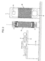
Fig. 2 is a diagram schematically showing a
PET imaging apparatus and an X-ray CT imaging apparatus
of Fig. 1;
Fig. 3 schematically shows a sectional view
along the circumferential direction of the PET imaging
apparatus shown in FIG. 1;
Fig. 4 is a diagram schematically showing the
structure of the minimum configuration of a
semiconductor radiation detector;
Fig. 5 is a graph for comparing "time-peak
value curves" of a large thickness t and a small
thickness t for the semiconductor material of the
semiconductor radiation detector;
Fig. 6 is a graph schematically showing the
relationship of a thickness t of the semiconductor
material of the semiconductor radiation detector and a
peak value (maximum value);
Fig. 7 is a diagram schematically showing the
configuration of the semiconductor radiation detector
having a laminated structure of the semiconductor
material and electrodes (anode, cathode);
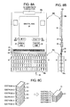
Fig. 8A is a front view showing a combined
substrate in which a detector substrate and an ASIC
substrate of the semiconductor radiation detector of
the present embodiment are combined;
Fig. 8B is a side view of Fig. 8A;
Fig. 8C is a perspective view schematically
showing the configuration of the semiconductor
radiation detector mounted on a detector substrate of
Fig. 8A;
Fig. 9 is a block diagram schematically
showing an analog detection circuit;
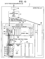
Fig. 10 is a block diagram which
schematically shows the configuration of a digital ASIC
and the connection relationship between an analog ASIC
and the digital ASIC;
Fig. 11 is a perspective view cited for
explaining the structure of a detector unit which
stores a plurality of semiconductor radiation
detectors;
Fig. 12 is a side view showing that a side
plate is removed from the detector unit of FIG. 11;
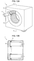
Fig. 13A is a partially cutaway perspective
view showing a state of mounting the detector unit in
the PET imaging apparatus;
Fig. 13B is a sectional view showing the
center of Fig. 13A;
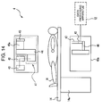
Fig. 14 is a diagram schematically showing an
X-ray CT imaging apparatus;
Fig. 15 is a diagram schematically showing a
sectional view along the circumferential direction of
the X-ray CT imaging apparatus shown in Fig. 14;
Fig. 16 is a block diagram schematically
showing a data processing apparatus;
Fig. 17 is a diagram showing an example of an
operation screen displayed on a display apparatus;
Fig. 18 is a diagram schematically showing
the configuration of the X-ray CT imaging apparatus
serving as a radiation examination apparatus according
to another embodiment;
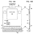
Fig. 19A is a front view showing a combined
substrate in which a detector substrate and an ASIC
substrate of the semiconductor radiation detector of
the present embodiment are combined;
Fig. 19B is a side view of Fig. 19A;
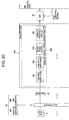
Fig. 20 is a block diagram schematically
showing an analog detection circuit;
Fig. 21 is a block diagram which
schematically shows the configuration of a digital ASIC
and the connection relationship between an analog ASIC
and the digital ASIC; and
Fig. 22 is a graph which shows simulation
results of 3D imaging and the relationship between an
energy threshold value and a scatter fraction.
DESCRIPTION OF THE EMBODIMENTS
The following will specifically describe a
radiological imaging system according to a preferred
embodiment of the present invention with reference to
the accompanying drawings. The following will discuss
a PET imaging apparatus which is a first imaging
apparatus constituting the radiological imaging system
of the present embodiment, an X-ray CT imaging
apparatus which is a second imaging apparatus, and
elements such as a semiconductor radiation detector
applied to the present embodiment.
[Embodiment 1]
As shown in Figs. 1 and 2, the radiological
imaging system of the present embodiment has two
independent gantries which comprise a bed 14 serving as
a berthing apparatus, a PET imaging apparatus 1 serving
as a first imaging apparatus, and an X-ray CT imaging
apparatus 4 serving as a second imaging apparatus. As
shown in Fig. 1, the radiological imaging system
includes a data processing apparatus 12 and a display
apparatus 13. An examinee (subject) H is loaded on the
bed 14 which can move forward and backward along the
body axis direction (X1 and X2 directions) of the
examinee H, and the examinee H is imaged by the PET
imaging apparatus 1 and the X-ray CT imaging apparatus
4.
A. (PET imaging apparatus)
The PET imaging apparatus 1 includes a number
of semiconductor radiation detectors 21 (Figs. 4, 8,
11). γ-rays radiated from the inside of the examinee H
are detected by the semiconductor radiation detectors
(hereinafter, simply referred to as detectors) 21. The
PET imaging apparatus 1 has an integrated circuit
(ASIC) for measuring a peak value of the γ-ray and
detection time, so that the peak value and detection
time of the detected radiation (γ-ray) are measured.
As shown in Fig. 3, in the PET imaging
apparatus 1, a number of detector units 2 (specifically
shown in Fig. 11) are arranged like a circle to detect
a γ-ray radiated from the examinee H. The detector unit
2 stores a plurality of combined substrates 20
(specifically shown in Figs. 8A and 8B) each of which
has a number of detectors 21. The examinee H serving
as a subject lies on the bed 14 so as to be positioned
at the center of the PET imaging apparatus 1. At this
point, the detectors 21 surround the bed 14. From the
detector units 2, γ-ray peak value information and γ-ray
detection time information that are obtained based on a
detection signal when the detectors 21 interact with γ-rays,
and the address information (detector ID) of the
detector 21 are outputted for each of the detectors 21
included in the detector unit 2. The configurations of
the detector 21, the combined substrate 20, and the
detector unit 2 will be specifically described later.
Incidentally, radioactive chemicals, e.g.,
fluorodeoxyglucose (FDG) containing 18F having a half-life
of 110 minutes are administered to the examinee H.
From the body of the examinee H, γ-rays (annihilated γ-rays)
are radiated when positrons emitted from the FDG
are annihilated.
As shown in Fig. 1, the PET imaging apparatus
1 is formed with a smaller housing than that of the X-ray
CT imaging apparatus 4, which will be described
later, and the PET imaging apparatus 1 is disposed in
front of the X-ray CT imaging apparatus 4 in the body
axis direction (directions of X1 and X2 arrows in Fig.
1) of the examinee H.
The detail of the PET imaging apparatus 1
will be described below.
(Semiconductor radiation detector)
First, the detector 21 applied to the present
embodiment will be described below. As shown in Fig.
4, the detector 21 is configured (minimum
configuration) so that both sides of a semiconductor
radiation sensor (hereinafter, referred to as a sensor)
211 composed of a plate-like semiconductor material S
are covered with electrodes (anode A, cathode C) shaped
like thin plates (films). In this configuration, the
semiconductor material S is composed of any one of
single crystals including CdTe (cadmium telluride),
TlBr (thallium bromide), and GaAs (gallium arsenide).
Further, the electrodes (anode A, cathode C) are made
of any one of materials including Pt (platinum), Au
(gold), and In (indium). In the following explanation,
the semiconductor material S composed of a single
crystal of CdTe is sliced. Moreover, a detecting
radiation is a γ-ray of 511 KeV that is used in the PET
imaging apparatus 1.
Referring to Fig. 4, the detection principle
of a γ-ray in the detector 21 will be schematically
described below. When a γ-ray is incident on the
detector 21 and the γ-ray and the semiconductor material
S constituting the detector 21 interact with each
other, holes and electrons (schematically indicated as
"+" and "-" in Fig. 4) are generated in pairs up to an
amount in proportion to the energy of the γ-ray. In
this configuration, voltage for collecting charge is
applied across the electrodes of the anode A and the
cathode C of the detector 21 (e.g., 300V). Thus, the
holes are attracted to the cathode C and the electrons
are attracted to the anode A. According to a
comparison between the holes and the electrons, the
electrons have relatively higher mobility and thus the
electrons reach the anode in a relatively short time.
On the other hand, the holes have relatively low
mobility and thus the holes reach the cathode in a
relatively long time. Incidentally, the holes may
disappear before reaching the electrode.
As shown in Fig. 5 in which the "time - peak
value curves" are compared with each other regarding a
large thickness and a small thickness of the
semiconductor material S of the detector 21 (sensor
211), the semiconductor material S with the smaller
thickness t rises in peak value more quickly and has a
higher peak value. A quickly rising peak value
contributes to, for example, higher accuracy of
coincidence detection in the PET. Further, a high peak
value contributes to a higher energy resolution. In
this way, the smaller thickness t increases a peak
value more quickly and achieves a higher peak value
(higher efficiency of collecting charge). This is
because the electrons and holes reach the electrodes
(anode A, cathode C) in a short time (time of
collecting charge). Another reason is that the holes
which may disappear on their way can reach the
electrode (cathode C) due to a short distance without
disappearance. Incidentally, the thickness t can be
also expressed as a distance between the electrodes of
the anode A and the cathode C which face each other.
The sensor 211 preferably has a thickness
(distance between the electrodes) t of 0.2 to 2 mm.
When the thickness t is 2 mm or larger, a peak value
rises slowly and becomes lower. Meanwhile, when the
thickness t is 0.2 mm or smaller, the thicknesses
(volumes) of the electrodes (anode, cathode) relatively
increase. In the case of installation on a substrate,
the important semiconductor material S to interact with
a radiation decreases in ratio. That is, when the
thickness t of the semiconductor material S is reduced,
the electrode not interacting with a γ-ray relatively
increases in thickness and meanwhile the semiconductor
material S interacting with the γ-ray relatively
decreases in ratio, resulting in lower sensitivity for
detecting the γ-ray (the γ-ray passes by the sensor).
Further, when the thickness t is small, a number of
leak currents occur and do not permit the application
of high voltage for collecting charge.
For the same reason, it is more preferably
that the semiconductor material S has a thickness t of
0.5 to 1.5 mm. The preferable thickness t more
positively enables detection of a γ-ray and a more
accurate measurement of a peak value.
Since the PET imaging apparatus 1 conducts a
coincidence detection, it is necessary to accurately
measure the time of detection of a γ-ray. For example,
in Fig. 4, the detection time is changed depending upon
whether the interaction position of the γ-ray and the
semiconductor material S is closer to the cathode C or
the anode A. That is, since the holes move at low
speed, an interaction occurring closer to the anode A
causes relatively late detection. An interaction
occurring closer to the cathode C causes relatively
early detection (closer to real time). That is, even
when a γ-ray interacts with semiconductor material S in
the same sensor 211, the detection time is changed by
the interaction position. To be specific, a large
thickness t causes a large difference of the detection
time depending upon the interaction position. Although
such a phenomenon is not a serious problem in other
fields, the PET imaging apparatus 1 for conducting a
coincidence detection on the order of nsec (nanosecond)
has a serious problem. Therefore, in this sense, the
detection time can be properly determined in the range
of thicknesses as described above. The detection time
of the PET imaging apparatus 1 is determined by LET
method and CFD method.
As shown in Fig. 6 schematically illustrating
the relationship between a peak value (maximum value)
and a thickness t of the semiconductor material S of
the detector 21, the larger the thickness t of the
semiconductor material S, the smaller the peak value.
The reason why the peak value decreases is, for
example, is that the holes disappear before reaching
the electrodes. When the thickness t is 2 mm or
larger, the peak value of a detected radiation becomes
smaller than a threshold value for discriminating a γ-ray
of 511 KeV. Thus, as described above, it is not
preferable to increase the thickness t of the
semiconductor material S to more than 2 mm.
As shown in Fig. 7, the detector 21 has the
semiconductor material S laminated into five layers
each of which is disposed between the cathode C and the
anode A (sensor 211). The detector 21 is a single-layer
detector in which each layer of the semiconductor
material S has the above-described thickness t (0.2 to
2 mm (more preferably 0.5 to 1.5 mm)). The anode A and
the cathode C are about 20 µm in thickness.
Incidentally, in the detector 21 having the laminated
structure of Fig. 7, since the anodes A are connected
to one another and the cathodes C are connected to one
another, each layer does not detect a radiation
separately from the other layers. In other words, when
a γ-ray and the semiconductor material S interact with
each other, it is not decided whether the interaction
occurs in the top layer or the bottom layer. As a
matter of course, detection may be carried out in each
layer. Incidentally, the five-layer structure is
constructed for the following reason: When the
thickness t of the semiconductor material S is small, a
peak value increases quickly to a higher value but more
γ-rays pass through the material in the smaller
thickness t, whereas the five-layer structure can
reduce the number of γ-rays passing through the material
to increase interactions between the semiconductor
material S and the γ-rays (to increase the number of
counts) while increasing the efficiency of collecting
charge.
With the detector 21 having the laminated
structure, it is possible to obtain a more preferable
increase rate (rise) in peak value and a more accurate
peak value, and increase the number of γ-rays (the
number of counts) interacting with the semiconductor
material S (increase sensitivity).
The detector 21 does not always have to have
such a laminated structure. A single-layer structure
is also applicable and two to four layers may be
provided for a properly layered structure.
The electrodes (anode A, cathode C)
preferably have an area s of 4 to 120 square
millimeters. An increase in the area s increases a
capacitance (stray capacitance) of the detector 21.
Noise is more likely to be superimposed due to the
increased stray capacitance. Thus, it is preferable to
minimize the electrode area s. Further, charge
generated during the detection of γ-rays is partly
accumulated in the stray capacitance and thus the
increased stray capacitance reduces charge accumulated
in a charge-sensitive amplifier 24b of an analog ASIC
24 (Fig. 9) and reduces an output voltage (peak value).
When CdTe is used as the detector 21, the detector 21
has a relative dielectric constant of 11. When the
detector 21 has the area s of 120 square millimeters
and the thickness t of 1 mm, the capacitance is 12 pF
which is not negligible in consideration of a
connectors and the like having a stray capacitance of
several pF in a circuit. Therefore, it is preferable
that the electrode area s is 120 square millimeters or
smaller.
Further, the lower limit value of the
electrode area s is determined by the position
resolution of the PET imaging apparatus 1. The
position resolution of the PET imaging apparatus 1 is
determined by the range of positrons and so on in
addition to the size (array pitch) of the detector 21.
Since a positron of 18F has a range of 2 mm, it is
useless to set the size of the detector 21 at 2 mm or
smaller. A packaging method for minimizing the
electrode area is to arrange an electrode surface
perpendicularly to the radius direction of the PET
imaging apparatus 1. According to the above
consideration, the lower limit value of one side of the
electrode is 2 mm and the lower limit value of the
electrode area s is 4 square millimeters.
In the above explanation, the semiconductor
material S interacting with a γ-ray was CdTe. It is
needless to say that the semiconductor material S may
be TlBr and GaAs. Further, although the words of "the
laminated structure", "top layer" and "bottom layer"
were used, the words are used with reference to Fig. 7.
When Fig. 7 is seen after being rotated by 90°, "the
laminated structure" may be replaced with a "parallel
structure" and the "top and bottom layers" may be
replaced with "right and left layers." The direction
of γ-ray incidence may be from the top, bottom, left, or
right of Fig. 7. In other words, the detector 21 is
configured so that the plurality of (e.g., five)
semiconductor material S are arranged in parallel in
such a manner as to be sandwiched between the cathode C
and the anode A.
(Combined substrate)
Referring to Fig. 8, the following will
describe the detailed structure of the combined
substrate (unit substrate) 20 mounted in the detector
unit 2 (Fig. 11). The combined substrate 20 has a
detector substrate (first substrate) 20A having the
plurality of detectors 21, and an ASIC substrate
(second substrate) 20B having capacitors 22, resistors
23, analog ASICs 24, analog/digital converters (AD
converters, hereinafter referred to as ADC) 25, a
digital ASIC 26.
(Detector substrate)
Referring to Figs. 8A-8C, the detector
substrate 20A having the detectors 21 will be described
below. As shown in Fig. 8A, in the detector substrate
20A, the plurality of detectors 21 are arranged and
mounted (packaged) in a lattice pattern on one side of
the substrate body 20a (four lines of the 16 detectors
21, that is, 4 × 16 = 64 in total). In the radius
direction of the PET imaging apparatus 1, four lines of
the detectors 21 are arranged on a substrate body 20a.
The above-described 16 detectors 21 are arranged in the
axial direction of the PET imaging apparatus 1, that
is, in the longitudinal direction (directions of moving
forward and backward) of the bed 14. Further, as shown
in Fig. 8B, the detectors 21 are attached on both sides
of the detector substrate 20A and thus each of the
detector substrates 20A has a total of 128 detectors
21. As the attached detectors 21 increases in number,
γ-rays can be more readily detected with higher accuracy
of position. Thus, the detectors 21 are arranged on
the detector substrate 20A as densely as possible.
Incidentally, when γ-rays radiated from the examinee H
(Fig. 3) on the bed 14 move from below to above (the
direction of an arrow 32, i.e., the radius direction of
the PET imaging apparatus 1) in Fig. 8A, it is
preferable to arrange the detectors 21 densely in the
lateral direction of the detector substrate 20A in
order to reduce the number of γ-rays passing though the
detectors 21 (the number of γ-rays passing through gaps
between the detectors 21). Hence, it is possible to
improve the efficiency of detecting γ-rays, thereby
increasing the spatial resolution of an obtained image.
As shown in Fig. 8B, the detector substrate
20A of the present embodiment has the detectors 21
attached to both sides of the substrate body 20a.
Thus, unlike a detector substrate having detectors only
on one side, the substrate body 20a can be used in a
shared manner by mounting the detectors 21 on both
sides. Hence, it is possible to reduce the number of
the substrate bodies 20a by half and arrange the
detectors 21 more densely in the circumferential
direction. In addition, as described above, since the
number of the detector substrates 20A (combined
substrates 20) can be reduced by half, it is possible
to save time and trouble to attach the combined
substrates 20 to a housing 30 (Fig. 11), which will be
discussed later.
In the above explanation, the 16 detectors 21
across the substrate are arranged in the axial
direction of a camera 11. The configuration is not
particularly limited. For example, the 16 detectors 21
across the substrate may be arranged in the
circumferential direction of the camera 11.
As shown in Fig. 8C, each of the detectors 21
has a laminated structure where the single crystals of
the semiconductor material S (sensor 211) are laminated
like above-described thin plates. A supplementary
explanation will be given below about the configuration
and operation which have been discussed with reference
to Fig. 7. As described above, the detector 21 has the
anodes A and the cathodes C. A potential difference
(voltage) such as 300 V is set across the anode A and
the cathode C in order to collect charge. This voltage
is supplied from the ASIC substrate 20B to the detector
substrate 20A via a connector C1 (Fig. 8A). Further, a
signal detected by the detector 21 is supplied to the
ASIC substrate 20B via the connector C1. Hence, in the
substrate body 20a of the detector substrate 20A, a
intra-substrate wiring (not shown, for collecting
charge and for transmitting and receiving a signal)
which connect the connector C1 and the detectors 21,
are provided. Besides, the intra-substrate wiring has
a multilayered structure. In the present embodiment,
the sensors 211 of the detector 21 are arranged in
parallel with the substrate body 20a. The detector 21
may be attached so that the sensors 211 are arranged
perpendicularly to the substrate body 20a.
(ASIC substrate)
The ASIC substrate 20B having the ASIC will
be described below. As shown in Fig. 8A, the ASIC
substrate 20B has the two analog ASICs 24 and one
digital ASIC 26 on one side of the substrate body 20b.
As shown in Fig. 8B, since the analog ASICs 24 are
attached on both sides of the substrate body 20b, the
ASIC substrate 20B has a total of four analog ASICs 24.
Further, the ASIC substrate 20B has the eight (=4x2)
ADCs 25 on one side of the substrate body 20b and the
16 ADCs 25 on both sides of the substrate body 20b.
Moreover, on both sides of the substrate body 20b, the
capacitors 22 and the resistors 23 are arranged as many
as the detectors 21. Like the detector substrate 20A,
the ASIC substrate 20B (substrate body 20b) has intra-substrate
wiring (not shown) to electrically connect
the capacitors 22, the resistors 23, the analog ASICs
24, the ADCs 25, and the digital ASIC 26. The intra-substrate
wiring also has a laminated structure.
In the arrangement (intra-substrate wiring)
of the elements 22, 23, 24, 25, and 26, a signal
supplied from the detector substrate 20A is sent to the
capacitors 22, the resistors 23, the analog ASICs 24,
the ADCs 25, and the digital ASIC 26 in this order.
Additionally, the ASIC substrate 20B has the
connector (spiral contact) C1 which is connected to the
intra-substrate wiring connected to the capacitors 22
and makes an electrical connection with the detector
substrate 20A, and a substrate connector C2 which makes
an electrical connection with the data processing
apparatus (integrated FPGA, described later).
Incidentally, the above-described detector substrate
20A also has the connector C1 which is connected to the
intra-substrate wiring connected to the detectors 21.
The analog ASIC is an ASIC (Application Specific
Integrated Circuit) which is a kind of LSI and is an IC
for a specific application of processing an analog
signal.
(Connecting structure of the detector substrate and the
ASIC substrate)
The following will describe the connecting
structure of the detector substrate 20A and the ASIC
substrate 20B.
Instead of connecting the detector substrate
20A and the ASIC substrate 20B by butt-joining the end
faces (ends), as shown in Fig. 8B, overlapping portions
are provided near the ends to connect the connectors C1
attached to the overlapping portions. This connection
is made in a detachable/attachable manner (is freely
separated and connected) by a fastening screw. Such a
connection is made for the following reason: when one
or both ends of the combined substrate 20 is
horizontally supported, which has the detector
substrate 20A and the ASIC substrate 20B connected
(joined) to each other, force distorting or bending
down the combined substrate 20 is applied to the center
(connected part) of the combined substrate 20. When
the connected part has butted end faces, the connected
part is readily distorted or bent. Hence, butted-joined
end faces are not preferable.
In consideration of this point, in the
present embodiment, instead of connecting the detector
substrate 20A and the ASIC substrate 20B by butt-joining
the end face, a connection is made by providing
the overlapping portions where the ends overlap each
other as described above. Thus, as compared with the
butt-joined end faces, such a connection is preferable
because a resistance to distortion and bending is
improved. When the combined substrate increases the
resistance to distortion and bending, for example, the
displacement of the detector 21 is reduced so as to
prevent a reduction in the accuracy of locating the
occurrence of a γ-ray. As shown in Fig. 3, the PET
imaging apparatus 1 has a number of detector units 2
(Fig. 11) which have the combined substrates 20 of Fig.
8A and are arranged like a donut. Thus, the combined
substrates 20 disposed at 3 o'clock and 9 o'clock
positions in the horizontal direction of Fig. 3 are
readily distorted or bent. For this reason, it is
important for the combined substrate 20 to obtain
resistance to distortion and bending.
The detector substrate 20A and the ASIC
substrate 20B are electrically connected to each other
by using the overlapping portions as described above.
Thus, the connector C1 (Fig. 8A) for electrically
connecting the intra-substrate wirings of the
substrates 20A and 20B is provided on each of the
overlapping portions of the detector substrate 20A and
the ASIC substrate 20B of Fig. 8B. For example, a
spiral contact (R) is used as the connector C1 to
preferably make an electrical connection. The spiral
contact (R) is characterized in that a connecting
terminal shaped like a ball makes contact with a spiral
contact through a wide area so as to preferably make an
electrical connection. When the connecting terminal
shaped like a ball is provided on the ASIC substrate
20B, the spiral contact is provided on the detector
substrate 20A. When the connecting terminal shaped
like a ball is provided on the detector substrate 20A,
the spiral contact is provided on the ASIC substrate
20B.
Since the detector substrate 20A and the ASIC
substrate 20B are electrically connected to each other
in such a manner, a signal can be transmitted from the
detector substrate 20A to the ASIC substrate 20B with
low loss. Lower loss increases, for example, the
energy resolution of the detector 21.
As described above, the detector substrate
20A and the ASIC substrate 20B are connected to each
other via a screw and the like in a
detachable/attachable manner. Therefore, for example,
even when the detectors 21 and the ASICs 24 and 26 have
defects, it is only necessary to replace defective
parts. Thus, it is possible to eliminate waste of the
replacement of the overall combined substrate 20 even
in the event of a defective part. Further, the
detector substrate 20A and the ASIC substrate 20B are
electrically connected to each other via the connector
C1 such as the above-described spiral connector (R),
thereby readily connecting/disconnecting
(coupling/decoupling) the substrates.
In the above configuration, one detector
substrate 20A is connected to the ASIC substrate 20B.
The detector substrate may be divided into two or more.
For example, the following configuration is applicable:
the detectors 21 in eight columns and four rows are
packaged on one substrate and two detector substrates
are connected to the ASIC substrate. In this
configuration, when one of the detectors 21 is failed,
it is only necessary to replace the detector substrate
having the failed detector out of the two detector
substrates, thereby reducing waste in maintenance
(reducing cost).
(Layout of elements)
Referring to Figs. 8A and 9, the following
will describe the layout of the elements such as the
detectors 21 and the ASICs 24 and 26 on the combined
substrate 20.
As shown in Fig. 9, the detector 21 is
connected to the analog ASIC 24 via the connector C1,
the capacitor 22, and the resistor 23 by using
electrical wiring (not shown). A detection signal of a
γ-ray detected by the detector 21 passes through the
capacitor 22 and the resistor 23 via the electrical
wiring and is processed in the analog ASIC 24.
Further, the signal processed in the analog ASIC 24 is
processed in the ADC 25 and the digital ASIC 26.
In this case, a short circuit and short
wiring (distance) are preferable because the influence
of noise and the attenuation of a signal are reduced in
the processing. Further, when a coincidence detection
is conducted in the PET imaging apparatus 1, a shorter
circuit and shorter wiring are preferable because a
delay is reduced (preferable because the accuracy of
detection time is not reduced). Thus, in the present
embodiment, the detectors 21, the capacitors 22, the
resistors 23, the analog ASICs 24, the ADCs 25, and the
digital ASIC 26 are arranged (laid out) in this order
from the axis to the outside in the radius direction of
the PET imaging apparatus 1 as shown in Fig. 8A. This
order is the same as the signal processing order
performed by the elements 21, 22, 23, 24, 25, and 26
(Figs. 9 and 10). That is, from the axis of the camera
11 to the outside, "detectors, analog integrated
circuits, AD converters, and a digital integrated
circuit are arranged in this order on a substrate and
wiring is carried out in this order." In other words,
the order of arranging the elements 21, 22, 23, and 24
from the detectors 21 to the digital ASIC 24 matches
with the signal processing order of the elements 21,
22, 23, and 24. Hence, a weak signal detected by the
detector 21 can be transmitted to the analog ASIC 24 by
reducing the length of the wiring (distance).
Since processing such as the amplification of
a signal is performed in the analog ASIC 24, even when
wiring after the analog ASIC 24 is long, a signal is
less susceptible to noise. That is, in consideration
of noise, no problem occurs even if wiring after the
analog ASIC 24 is long. However, as described above,
long wiring delays the transmission of a signal and
thus the accuracy of detection time may be reduced.
In the present embodiment, since one combined
substrate 20 includes the analog ASICs 24 and the
digital ASIC 26 as well as the detectors 21, it is
possible to arrange the detectors 21, the analog ASICs
24, and the digital ASIC 26 in the perpendicular
direction of the bed 14, that is, orthogonally to the
body axis of the examinee H to be examined. Thus, the
length of the PET imaging apparatus 1 in the
longitudinal direction of the bed 14 does not have to
be increased more than necessary. It can be considered
that the analog ASICs 24 and digital ASICs 26 is
disposed along the longitudinal direction of the bed 14
on the outer side of the radius direction of the
detectors arranged like a ring. However, the PET
imaging apparatus 1 becomes longer than necessary in
the longitudinal direction of the bed 14. Moreover, a
semiconductor radiation detector is used as the
detector 21, and the analog ASIC 24 and the digital
ASIC 26 are used as signal processors. Thus, it is
possible to reduce a length in the longitudinal
direction of the combined substrate 20 and considerably
reduce a length in the orthogonal direction of the PET
imaging apparatus 1 as compared with the case where a
scintillator is used. Further, since the combined
substrate 20 has the detectors 21, the analog ASICs 24,
and the digital ASIC 26 which are arranged in this
order along the longitudinal direction of the combined
substrate 20, the wiring for connecting the elements
can be shortened and the wiring of the substrate can be
simplified. Therefore, it is possible to achieve the
PET imaging apparatus 1 contributing to
miniaturization.
In the present embodiment, one analog ASIC 24
is connected to the 32 detectors 21 to process signals
obtained from the detectors 21. As shown in Figs. 9
and 10, one analog ASIC 24 comprises 32 sets of analog
signal processing circuits (analog signal processing
apparatus) 33 made up of a slow system and fast system.
The analog signal processing circuit 33 is provided for
each of the detectors 21 and is connected to one
detector 21. The fast system comprises a timing pick
off circuit 24a to output a timing signal for
identifying a detection time of γ-rays. The slow system
comprises a charge amplifier (preamplifier) 24b, a
polarity amplifier (linear amplifier) 24c, a band pass
filter (waveform shaping apparatus) 24d and a peak hold
circuit (peak value holding apparatus) 24e connected in
this order for the purpose of calculating a peak value
of the detected γ-rays. Note that the slow system is
named "slow" because it takes a certain degree of
processing time to calculate a peak value. A γ-ray
detection signal outputted from the detector 21 and
passed through the capacitor 22 and resistor 23 is
amplified in the charge amplifier 24b and polarity
amplifier 24c. The amplified γ-ray detection signal is
passed through the band pass filter 24d and inputted to
the peak hold circuit 24e. The peak hold circuit 24e
holds a maximum value of the detection signal, that is,
the peak value of a γ-ray detection signal proportional
to energy of the detected γ-rays. One analog ASIC 24 is
an LSI which integrates 32 sets of analog signal
processing circuits 33.
The capacitor 22 and resistor 23 can also be
provided inside the analog ASIC 24, but this embodiment
arranges the capacitor 22 and resistor 23 outside the
analog ASIC 24 for reasons such as obtaining an
appropriate capacitance and appropriate resistance and
reducing the size of the analog ASIC 24. The capacitor
22 and resistor 23 are preferably disposed outside
because variations in the individual capacitance and
resistance are reduced.
In the analog ASIC 24 shown in Fig. 9, the
output of the slow system of this analog ASIC 24 is
supplied to the ADC (analog/digital converter) 25 in
the present embodiment. Moreover, the output of the
fast system of the analog ASIC 24 is designed to be
supplied to the digital ASIC 26.
The analog ASIC 24 and each ADC 25 are
connected via one wire which sends slow system signals
corresponding to 8 channels all together. Furthermore,
each analog ASIC 24 and digital ASIC 26 are connected
via 32 wires which send 32-channel fast system signals
one by one. That is, one digital ASIC 26 is connected
to four analog ASICs 24 via a total of 128 wires.
The output signal of the slow system
outputted from the analog ASIC 24 is an analog peak
value (maximum value of the graph shown in Fig. 5).
Further, the output signal of the fast system outputted
from the analog ASIC 24 to the digital ASIC is a timing
signal indicating timing corresponding to the detection
time. Of these signals, the peak value which is the
slow system output is inputted to the ADC 25 via the
wire (wire uniting 8 channels into one as described
above) connecting the analog ASIC 24 and ADC 25 and is
converted to a digital signal by the ADC 25. The ADC
25 converts a peak value to, for example, an 8-bit (0
to 255) digital peak value (e.g., 511 KeV→255).
Moreover, a timing signal serving as the output of the
fast system is supplied to the digital ASIC 26 via the
wire connecting the analog ASIC 24 and digital ASIC 26.
The ADC 25 sends the digitized 8-bit peak
value information to the digital ASIC 26. For this
purpose, each ADC 25 and digital ASIC 26 are connected
via a wire. For example, since there are 16 ADCs 25 on
both sides, the digital ASIC 26 is connected to the ADC
25 via a total of 16 wires. One ADC 25 processes
signals corresponding to 8 channels (signals
corresponding to eight detection elements). The ADC 25
is connected to the digital ASIC 26 via a wire for
transmitting an ADC control signal and a wire for
transmitting peak value information.
As shown in Fig. 10, the digital ASIC 26
comprises a plurality of packet data generation
apparatuses 34, each of which includes eight time
decision circuits (time decision apparatuses) 35 and
one ADC control circuit (ADC control apparatus) 36, and
a data transfer circuit (data transmission apparatus)
37. All these elements are integrated into one LSI.
All the digital ASICs 26 provided in the PET imaging
apparatus 1 receive a 500 MHz clock signal from a clock
generation apparatus (crystal oscillator, not shown)
and operates synchronously. The clock signal inputted
to each digital ASIC 26 is inputted to the respective
time decision circuits 35 in all the packet data
generation apparatuses 34. The time decision circuit
35 is provided for each of the detectors 21 and
receives a timing signal from the timing pick off
circuit 24a of the corresponding analog signal
processing circuit 33. The time decision circuit 35
determines the detection time of γ-rays based on the
clock signal when the timing signal is inputted. Since
the timing signal is based on the fast system signal of
the analog ASIC 24, a time close to a real detection
time can be set as the detection time (time
information).
The ADC control circuit 36 receives a timing
signal at which γ-rays are detected from the time
decision circuit 35 and identifies the detector ID.
That is, the ADC control circuit 36 stores a detector
ID corresponding to each time decision circuit 35
connected to the ADC control circuit 36 and can
identify, when time information is inputted from a
certain time decision circuit 35, the detector ID
corresponding to the time decision circuit 35. This is
possible because the time decision circuit 35 is
provided for each of the detectors 21. Moreover, after
inputting the time information, the ADC control circuit
36 outputs an ADC control signal including detector ID
information to the ADC 25. The ADC 25 converts, to a
digital signal, the peak value information outputted
from the peak hold circuit 24e of the analog signal
processing circuit 33 corresponding to the detector ID,
and the ADC 25 outputs the information. The peak value
information is inputted to the ADC control circuit 36.
The ADC control circuit 36 adds the peak value
information to the time information and detector ID to
create packet data. The packet data (including
detector ID, time information, and peak value
information) outputted from the ADC control circuit 36
of each packet data generation apparatus 34 is inputted
to the data transfer circuit 37.
The data transfer circuit 37 sends packet
data, which is digital information outputted from the
ADC control circuit 36 of each packet data generation
apparatus 34, to the integrated circuit (unit
combination FPGA (Field Programmable Gate array) 31)
for unit combination that is provided for the housing
30 of the detector unit 2 (Figs. 11 and 12) which
houses twelve combined substrates 20, for example,
periodically. The unit combination FPGA (hereinafter
referred to as "FPGA") 31 outputs the digital
information to an information transmission wire
connected to the connector 38.
In this way, packet data which is outputted
from the digital ASIC 26 and includes detector IDs for
uniquely identifying (1) peak value information, (2)
determined time information and (3) detector 21 is sent
to a PET data processing section 12a (Fig. 16) of the
data processing apparatus 12 (Fig. 1) of the subsequent
stage through the information transmission wire. The
coincidence detection apparatus 12A of the PET data
processing section 12a carries out coincidence
detection processing (when two γ-rays with predetermined
energy are detected with a time window with a set time,
this processing regards these γ-rays as a pair of γ-rays
generated by annihilation of one positron) based on the
packet data sent from the digital ASIC 26, counts the
simultaneously measured pair of γ-rays as one γ-ray and
locates, by using the detector IDs, the two detectors
21 which have detected the pair of γ-rays. When there
are three or more γ-ray detection signals detected
within the above time window (when there are three or
more detectors 21 which have detected γ-rays), the PET
data processing section 12a identifies the two
detectors 21 into which γ-rays are incident first out of
three or more detectors 21 using peak value
information, etc., on these γ-ray detection signals.
The identified pair of detectors 21 is simultaneously
measured and one count value (first information) is
generated. Further, a tomographic information creation
apparatus 12B of the PET data processing section 12a
creates tomographic information on the examinee at the
position where radiopharmaceuticals are concentrated,
that is, position of malignant tumor, using count
values obtained by coincidence detection and position
information (second information) on the detectors 21.
This tomographic information is displayed on the
display apparatus 13. Information such as the above
digital information, count values obtained by
coincidence detection, position information on the
detectors 21 and tomographic information are stored in
the storage apparatus of the data processing apparatus
12.
In the above described explanations, the
detector substrate 20A has the detectors 21 and the
ASIC substrate 20B has the capacitors 22, the resistors
23, the analog ASICs 24, the ADCs 25, and the digital
ASIC 26. The detector substrate (first substrate) 20A
may have the detectors 21, the capacitors 22, the
resistors 23, and the analog ASICs 24, etc., and the
ASIC substrate (second substrate) 20B may have the ADCs
25 and the digital ASIC 26, etc. By the detector
substrate 20A having the detectors 21 and the analog
ASICs 24, the distance (wire length) between the
detector 21 and analog ASIC 24 can be further
shortened. Thus, it is possible to further reduce the
influence of noise.
Furthermore, the combined substrate 20 may
include three substrates (detector substrate 20A,
analog ASIC substrate and digital ASIC substrate) which
may be connected in a detachable/attachable manner
through their respective connectors. The detector
substrate 20A has the detectors 21, the analog ASIC
substrate has the capacitors 22, the resistors 23, and
the analog ASICs 24, and the digital ASIC substrate has
the ADCs 25 and the digital ASIC 26. This
configuration separates the substrate incorporating the
analog circuit from the substrate incorporating the
digital circuit to prevent noise on the digital circuit
side from entering the analog circuit. Moreover, this
configuration separates the substrate incorporating the
analog ASIC from the substrate incorporating the
digital ASIC and connects the two substrates using a
detachable/attachable connector, and therefore even
when only the digital ASIC malfunctions, only the
digital ASIC substrate needs to be replaced. In this
way, this structure can further reduce waste.
In the above explanation, the substrate body
20a (detector substrate 20A) for mounting the detectors
21 is different from the substrate body 20b (ASIC
substrate 20B) for mounting the ASICs 24, 26. Thus,
when, for example, both ASICs are soldered to a
substrate by means of a BGA (Ball Grid Array) using
reflow, only the ASIC substrate can be soldered. This
is preferable because it is not necessary to expose the
detectors 21 to a high temperature. Of course, the
connector C1 may be omitted when all the components 21
to 26 are placed on the same substrate.
(Unit construction through housing of combined
substrate)
The following will describe a unit
construction where the combined substrate 20 is housed
in the housing 30. In the present embodiment, 12
combined substrates 20 are housed in the housing
(frame) 30 to constitute a detector unit (12 substrate
units) 2. The PET imaging apparatus 1 is configured so
that 60 to 70 detector units 2 are arranged in the
circumferential direction in a detachable/attachable
manner (Fig. 13B) so as to facilitate maintenance and
examination.
(Placement in housing)
As shown in Fig. 11, the detector unit 2
comprises a housing 30, etc., for housing or holding
the 12 combined substrates 20, a high-voltage power
supply PS for supplying a charge collecting voltage to
the 12 combined substrates 20, the FPGA 31, signal
connectors for exchanging signals with the outside, and
power connectors for receiving a power supply from the
outside.
As shown in Figs. 11 and 12, the combined
substrates 20 are housed in the housing 30, arranged in
three rows in the depth direction (longitudinal
direction of the bed 14) without overlapping with one
another and in four rows in the width direction
(circumferential direction of the PET imaging apparatus
1). That is, one housing 30 houses 12 combined
substrates 20. To realize such housing, a guide member
39 is disposed in the housing 30 and is attached to the
upper end of the housing (cover) 30. The guide member
39 consists of four rows of guide grooves (guide rails)
G1 which extend in the depth direction and are arranged
at appropriate intervals in the circumferential
direction. The guide member 39 has an opening 40
opposed to each connector C3 of a ceiling plate 30a in
the portion of each guide groove G1. Further, a bottom
surface 30b of the housing 30 is provided with four
guide members 41 each of which has one guide groove
(guide rail) G2 extending in the depth direction and
are arranged at appropriate intervals in the
circumferential direction (Fig. 12). The guide grooves
G1 and G2 have a depth corresponding to a capacity of
housing three combined substrates 20. An end of the
combined substrate 20 on the ASIC substrate 20B side is
housed in the guide groove G1 and an end of the
combined substrate 20 on the detector substrate 20A
side is housed in the guide groove G2. Three combined
substrates 20 are held in the depth direction of the
guide grooves G1, G2. Since the end of the combined
substrate 20 on the ASIC substrate 20B side and the
other end on the detector substrate 20A side slide in
the guide grooves G1 and G2, the combined substrates 20
can be readily positioned at predetermined points by
sliding the combined substrates 20 in the guide grooves
G1 and G2 with fingers. In this case, each substrate
connector C2 is disposed in the portion of each opening
40. After a predetermined number of combined
substrates 20 are arranged in the housing 30, the
ceiling plate 30a is attached at the top end of the
housing 30 in a detachable/attachable manner using
screws, etc. Each connector C3 provided on the ceiling
plate 30a is inserted in the corresponding opening 40
and is connected to the corresponding substrate
connector C2. The terms "upper" and "lower" parts of
the housing 30 are applicable when the housing 30 is
removed from the PET imaging apparatus 1, and when the
housing 30 is mounted in the PET imaging apparatus 1 as
shown in Figs. 13A and 13B, the upper and lower parts
may be inverted or turned 90 degrees to be "right" and
"left" parts or located diagonally.
As shown in Fig. 12, the ceiling plate 30a of
the housing 30 comprises not only the four rows of
guide grooves G1 but also FPGA 31 and connector 38.
The connector 38 is connected to the FPGA 31. The FPGA
31 is programmable in the field. In this aspect, the
FPGA 31 is different from the ASIC which is not
programmable. Therefore, as FPGA 31 with this
embodiment, even if the number or type of the combined
substrates 20 to be housed changes, it is possible to
properly respond to changes in the number of substrates
by programming in the field.
Since the detectors 21 containing CdTe as the
semiconductor material S in this embodiment generate
charge in reaction to light, the housing 30 is made of
a material such as aluminum and an alloy of aluminum
that have light shielding properties and the housing 30
is configured so as to eliminate gaps permitting the
entry of light. That is, the housing 30 has light
shielding properties. When light shielding properties
are secured by other means, the housing 30 itself does
not need light shielding properties and the housing 30
can be a frame (framework) to hold the detectors 21 in
a detachable/attachable manner (e.g., no light
shielding plane member (panel), etc., is necessary).
As shown in Fig. 13A, the detector unit 2 is
mounted via a unit support member 2A. Furthermore, as
shown in Fig. 13B, the detector unit 2 is mounted in
the PET imaging apparatus 1 with one end supported by
the unit support member 2A. The unit support member 2A
has a hollow disk (doughnut) shape and comprises many
windows (as many as the detector units 2 to be mounted)
in the circumferential direction of the PET imaging
apparatus 1. In order to support the detector units 2
at one end, a flange portion serving as a stopper is
provided on the front side in the axial direction of
the housing 30 of the detector unit 2. The flange
portions inside in the circumferential direction become
obtrusive when the detector units 2 are arranged as
dense as possible in the circumferential direction.
Therefore, the obtrusive flange portions may be removed
from the housing 30 to allow the flange portions
outside in the circumferential direction to remain.
Another unit support member 2A may be provided and both
ends of the detector unit 2 may be supported by the two
unit support members 2A.
When the detector units 2 is mounted in the
PET imaging apparatus 1, a cover 11a is removed to make
the unit support member 2A exposed and the detector
units 2 are inserted from the exposed portion until the
detector units 2 touch the flange portions. When the
detector units 2 are inserted and mounted, the PET
imaging apparatus 1 and the connectors of the detector
units 2 are connected to each other, and signals and
power supply are connected between the PET imaging
apparatus 1 and the detector units 2.
(Power supply)
The following will describe the high-voltage
power supply apparatus PS for supplying voltage for
collecting charge. As shown in Fig. 11, in the
detector unit 2, the high-voltage power supply
apparatus PS for supplying charge collection voltage to
each of the detectors 21 is provided in a space formed
inside the housing 30 on the back of the FPGA 31. This
high-voltage power supply apparatus PS receives a low
voltage power supply, boosts the voltage to 300 V using
a DC-DC converter (means for boosting the voltage, not
shown) and supplies the voltage to each of the
detectors 21. For each of the combined substrates 20
(= detector substrates 20A), 64 detectors 21 are
provided on one side and thus 128 detectors 21 are
provided on both sides. Twelve such combined
substrates 20 are housed in one housing 30 (that is,
one detector unit 2). Thus, the high-voltage power
supply apparatus PS supplies voltages to 128x12=1536
detectors 21.
Conventionally, a supply voltage of 300 V
with extremely small fluctuations is supplied from a
precision power supply apparatus in a remote place, but
(1) when the distance from the precision power supply
apparatus increases, a wider insulating structure for
high voltage wiring is required (the insulating
distance increases) accordingly and (2) the voltage
fluctuates due to a temperature variation of the
detectors 21, so that even the supply of a precise
voltage from the precision power supply apparatus does
not necessarily result in an expected precise voltage
in the desired target detectors 21.
Further, to facilitate maintenance and
examination, it is also considered that the detector
unit 2 of the present embodiment comprises a power
connector (not shown) and a high-voltage power line
extending from the precision power supply apparatus is
removed on the power connector. In the present
embodiment, it is considered that a high-voltage power
supply is supplied to the detector units 2 from the
outside of the units 2 via the power connector.
However, in the case of a high voltage of 300 V, the
power connector increases in size in addition to the
above described problem of insulation.
In the present embodiment, the high-voltage
power supply apparatus PS built in the detector unit 2
is connected to an external low voltage (5 to 15 V) DC
power supply through the power connector 42 and
connector 38 provided on the ceiling plate 30a via
power wiring. A high-voltage terminal of the high-voltage
power supply apparatus PS is connected to
twelve connectors C3, which are provided on the ceiling
plate 30a through the connector 43 provided on the
ceiling plate 30a, and is connected to electrodes C of
the detectors 21 provided on the substrate body 20a
through the connectors C2 of the combined substrates
20, power wiring (not shown) in the substrate body 20b,
the connector C1 and power wiring (not shown) in the
substrate body 20a. The connectors C1 and C2 include
not only connectors for transmitting output signals of
the detectors 21 but also connectors for power wiring.
Since the high-voltage power supply apparatus PS boosts
a low voltage applied from a direct-current power
supply to 300 V using a DC-DC converter, it is possible
to reduce the high-voltage section and thereby shorten
the insulation distance. That is, this eliminates the
necessity for using high-voltage wiring for a portion
from the connector 42 to the DC power supply. Further,
maintenance is facilitated. For the problem of
fluctuations in voltage, the present embodiment
comprises the high-voltage power supply apparatus PS
having accuracy according to a voltage changed by a
temperature, instead of the high-precision power supply
apparatus. Thus, it is possible to eliminate the
necessity for a high-precision power supply. Further,
since it is a low voltage that is received from an
external power supply, it is possible to use a small
power connector for the connector 38. The small power
connector increases the degree of freedom in the
layout. Further, since the high-voltage power supply
apparatus PS is arranged in a space formed in the
housing 30 on the back side of the FPGA 31, the
arrangement of the high-voltage power supply apparatus
PS in the housing 30 makes the detector unit 2 more
compact without upsizing. The high-voltage power
supply apparatus PS may be directly connected to the
power wiring provided on the substrate body 20a, via
the connector instead of the ceiling plate 30a. The
power connector may be separated from the output signal
connector of the detector 21. This configuration
prevents noise from entering the signal wiring from the
power supply system.
Further, by reducing a supply voltage to the
detector unit 2, it is possible to supply power to the
high-voltage power supply apparatus PS at a low voltage
through the unit combination FPGA 31 as with power
supplies to the ASICs 24, 26. Moreover, the supply of
power using the high-voltage power supply apparatus PS
eliminates the necessity for insulation from the
housing (GND) .
The voltage supplied to the high-voltage
power supply apparatus PS is boosted to 300 V by a DC-DC
converter (not shown) in the high-voltage power
supply apparatus PS and after boosting, passes through
the ceiling plate 30a of the housing 30, and is
supplied from the ASIC substrate 20B → detector
substrate 20A → each of the detectors 21 for each of
the combined substrates 20. That is, the housing 30
(ceiling plate 30a) comprises voltage supplying wiring
(not shown) for supplying a voltage from the high-voltage
power supply apparatus PS to each of the
combined substrates 20. Further, each of the combined
substrates 20 comprises voltage supplying wiring which
supplies a voltage supplied from the high-voltage power
supply apparatus PS to each of the detectors 21 via the
substrate connector C2.
B. (X-ray CT imaging apparatus)
As shown in Fig. 1, the X-ray CT imaging
apparatus 4 is disposed in the rear of the PET imaging
apparatus 1. As shown in Fig. 14, the X-ray CT imaging
apparatus 4 has radiation detectors 40, an X-ray source
circumferential moving apparatus 41, a drive controller
42, an X-ray source controller 43, and a casing 40a
(Fig. 15). Further, the X-ray source circumferential
moving apparatus 41 comprises a disk-like holding part
44, an X-ray source 45, and an X-ray source apparatus
holding part 45a. The X-ray source apparatus holding
part 45a is attached to the outer surface of the disk-like
holding part 44 on one end of the disk-like
holding part 44. The X-ray source 45 is attached to
the other end of the X-ray source apparatus holding
part 45a.
The radiation detector 40 arranges an X-ray,
which has passed through the examinee H from the X-ray
source 45, on a detectable position. A plurality of
(about 100) radiation detectors 40 are arranged from
the disk-like holding part 44 via a detector holding
part 46 and are rotated around the examinee H in
synchronization with the X-ray source circumferential
moving apparatus 41. Moreover, a collimator 47 is
attached to the radiation detector 40 and only an X-ray
generated from the X-ray source 45 is incident on the
radiation detector 40. In the present embodiment, the
radiation detector 40 is a scintillator detector.
The X-ray source 45 has a known X-ray tube
(not shown). The X-ray tube comprises in a housing, an
anode, a cathode, a current source of the cathode, and
a voltage source for applying voltage across the anode
and the cathode. The cathode is a filament made of
tungsten. Electrons are released from the cathode by
applying current from the current source to the
cathode. The electrons are accelerated by voltage (140
kV) applied across the cathode and the anode from the
voltage source and collide with the anode (W, Mo, etc.)
serving as a target. X-rays of 140 keV or lower are
generated when the electrons collide with the anode,
and released form the X-ray source 45.
The X-ray source controller 43 controls the
release time of X-rays from the X-ray source 45. That
is, in an X-ray CT examination, the X-ray source
controller 43 repeats the following control: an X-ray
generating signal is outputted to close a switch
(hereinafter referred to as an X-ray source switch, not
shown) provided between the power supply and the anode
(or cathode) of the X-ray tube in the X-ray source 45,
an X-ray stop signal is outputted after first setting
time to open the X-ray source switch, and the X-ray
source switch is closed after second setting time.
Across the cathode and the anode, voltage is applied
during the first setting time but is not applied during
the second setting time. With such control, X-rays are
released like pulses from the X-ray tube.
At the start of an X-ray CT examination, the
drive controller 42 outputs a drive start signal to
close a switch (hereinafter referred to as a first
motor switch, not shown) connected to the power supply.
A first motor is rotated by supplying current, the
turning force of the motor is transmitted to a pinion
via a power transmission mechanism, and thus the pinion
is rotated. The rotation of the pinion moves the disk-like
holding part 44, that is, the X-ray source 45
around the examinee H at a predetermined speed. At the
completion of the X-ray CT examination, the drive
controller 42 outputs the drive stop signal to open the
first motor switch. Thus, the X-ray source 45 is
caused to stop moving in the circumferential direction.
Since the radiation detectors 40 are fixed on the disk-like
holding part 44 via the detector holding part 46,
the radiation detectors 40 are rotated with the X-ray
source 45. Hence, when X-rays are radiated from the X-ray
source 45, the X-rays having passes through the
examinee H are measured by the radiation detectors 40.
The drive start signal having been outputted
from the drive controller 42 at the start of the X-ray
CT examination is inputted to the X-ray source
controller 43. The X-ray source controller 43 outputs
an x-ray generating signal based on the input of the
drive start signal. Thereafter, the X-ray stop signal
and the X-ray generating signal are repeatedly
outputted. In this way, since the X-ray stop signal
and the X-ray generating signal are repeatedly
outputted, the X-ray source 45 releases X-rays during
setting time (e.g., 1 µsec) and then stops releasing X-rays.
The release and stop of X-rays are repeated when
the X-ray source 45 moves in the circumferential
direction. The X-rays released from the X-ray source
45 are applied to the examinee H like fan beams. After
passing through the examinee H, the X-rays are
positioned apart from the X-ray source 45 and are
detected by the radiation detectors 40 beyond the
examinee H, rotated concurrently with the X-ray source.
The radiation detectors 40 output the detection signals
(hereinafter referred to as X-ray detection signals) of
the X-rays.
The above explanation discussed the method of
pulsed irradiation with X-rays. The method of
irradiation is not particularly limited and thus X-ray
may be applied continuously while charge accumulation
time is controlled upon measurement.
(Data processor)
As shown in Fig. 16, the data processing
apparatus 12 has the PET data processing section 12a
for processing data from the PET imaging apparatus 1
and an X-ray CT data processing section 12b for
processing data from the X-ray CT imaging apparatus 4.
Further, the data processing apparatus 12 includes a
PET/CT control section 12c.
The PET data processing section 12a has a
storage apparatus (not shown), a coincidence detection
apparatus 12A, and a tomographic information creation
apparatus 12B. The PET data processing section 12a
captures packet data including a peak value of detected
γ-rays, data of detection time, and detector (channel)
IDs. The coincidence detection apparatus 12A performs
coincidence detection based on the packet data,
particularly the data of detection time and the
detector IDs, identifies the detection positions of 511
keV γ-rays, and stores the positions in the storage
apparatus. The tomographic information creation
apparatus 12B creates a functional image based on the
identified positions and outputs the image. In the
case of two-dimensional imaging, it is preferable to
use a method such as filtered back projection as a PET
image reconstruction method. In the case of three-dimensional
imaging, an image is reconstructed by
using, e.g., Fourier rebinning discussed in IEEE
Transactions on Medical Imaging, vol. 16, page 145,
1997. Thus, a PET image is obtained. With the PET
image, it is possible to obtain occurrence density
information on a pair of γ-rays.
The X-ray CT data processing section 12b
includes an amplifier circuit 12C and a sample and hold
circuit 12D. The X-ray CT data processing section 12b
receives the X-ray detection signal from the radiation
detector 40 and converts the intensity of the X-ray
detection signal into data. Since X-rays released from
the X-ray source 45 are considerably higher in
incidence rate than the γ-rays, the X-ray CT data
processing section 12b is ordinarily constituted of a
so-called current mode (integration mode) measuring
circuit. X-ray detection signals (current signals)
from the radiation detectors 40 are accumulated by the
integral amplifier circuit 12C, and the sample values
of the signals are held by the sample and hold circuit
12D. These operations are repeated by a reset signal
in a predetermined period (maximum about several-ten
milli-seconds), so that the intensity of X-rays is
converted into data by the sample and hold circuit 12D
in each fixed time. As in the above-described case,
the method of reconstructing X-ray CT data is filtered
back projection method which is described in IEEE
transactions on Nuclear Science, NS-21 vol., page 21.
An obtained image has CT values in a cube or a cube
voxel which is set with equal sides in the x direction,
y direction, and z direction in a body.
The PET/CT control section 12c is constituted
of a computer or a work station and so on. The PET/CT
control section 12c creates a timing chart of a PET
examination and a CT examination therein, instructs the
bed 14, the PET imaging apparatus 1, the X-ray CT
imaging apparatus 4, the PET data processing section
12a, and the X-ray CT data processing section 12b to
perform desired operations based on the timing chart,
and reconstruct an X-ray CT image based on a tomogram
(PET image) and X-ray imaging data from the X-ray CT
data processing section 12b by using γ-ray imaging data
from the PET data processing section 12a. When the X-ray
CT image is obtained, a linear attenuation
coefficient in the examinee H between the X-ray source
45 and the radiation detectors 40 is determined using a
decrement of X-rays based on the X-ray imaging data. A
linear attenuation coefficient of each voxel is
determined by using the linear attenuation coefficient
according to a method such as filtered back projection.
Then, a CT value of each voxel is obtained using a
linear attenuation coefficient of each voxel. The X-ray
CT image data is obtained using these CT values.
Further, an absorbed amount of γ-rays of 511 keV is
calculated from the CT value, so that absorption in the
body of the examinee H is corrected and a correct PET
tomogram is reconstructed. The reconstructed tomograms
are both displayed by the display apparatuses 13.
Therefore, it is not necessary to provide a radiation
source for correcting absorption in the PET imaging
apparatus 1.
In this case, the PET image can be readily
combined with the X-ray CT image with accuracy by
aligning the axes of holes 50 (Fig. 2) in both of image
data. The images may be combined in sinogram data and
a frequency space. The combined tomograms which are
displayed by the display apparatus 13 include an X-ray
CT image. Thus, in the PET image, it is possible to
readily confirm the position of an affected area in the
body of the examinee H. That is, since the X-ray CT
image includes the image of internal organs and bones,
the position of an affected area (e.g., a cancer) can
be identified based on the positional relationship
between the internal organs and bones.
In the present embodiment, the PET imaging
apparatus 1 and the X-ray CT imaging apparatus 4 are
arranged along the length of the bed 14 (along the
axial direction of the examinee H). Thus, it is
possible to separately pick up the PET image from the
PET imaging apparatus 1 and the X-ray CT image from the
X-ray CT imaging apparatus 4 and prevents interference,
etc., from losing necessary data.
(Operations of the radiological imaging system)
The following will describe the operations of
the radiological imaging system configured thus.
Before a radiological examination,
radioactive chemicals for PET are first administered
beforehand to the examinee H by injection, etc., so
that an administered radiation is 370 MBq in the body.
The radioactive chemicals is selected according to the
objective of examination (to locate a cancer or to
conduct an examination of an aneurysm of a heart,
etc.). The examinee H stands by until the radioactive
chemical gathers so as to permit imaging. During a
predetermined time, the radioactive chemicals gather on
an affected area of the examinee H. After the
predetermined time, the examinee H is laid down on the
bed 14 (Fig. 2). In some kinds of examinations,
radioactive chemicals may be administered to the
examinee H laid down on the bed 14.
An examiner (a clinical radiographer and a
doctor) who performs a PET examination and a CT
examination inputs necessary information (an area
desired as a tomogram (imaged area or concerned area),
the number of slices, slicing intervals, the timing of
CT scanning, an absorbed dose, etc.) to the PET/
CT
control section 12c according to the objective of the
examination. The information input screen of Fig. 17
is displayed by the
display apparatus 13 to input
necessary data with a keyboard, a mouse, and so on. By
arranging combo boxes and radio buttons on the screen
as shown in Fig. 17, input can be readily performed.
In PET/CT control, a PET examination/CT examination
sequence (abbreviated as an "examination sequence" when
necessary) is created based on the inputted
information. When a "display button" is clicked on the
information input screen of Fig. 17, the examination
sequence is created in the PET/
CT control section 12c
and is displayed on the
display apparatus 13. When a
"start examination" button is clicked, an examination
is started. In the PET/
CT control section 12c, the
following parameters are all programmed in a series of
examination sequences and are performed at a time
determined by the number of clocks relative to the
reference time to start an examination.
The sequences (including movement control of
the bad 14) are made so as to switch imaging between
the PET imaging apparatus 1 and the X-ray CT imaging
apparatus 4.
Further, since the irradiation area of X-rays
spreads in the axial direction, switching is performed
while the radiation detectors 40 are arranged as a
group of about ten detectors at the maximum in the
axial direction. Incidentally, when the radiation
detector 40 is in a square form of 5 mm by 5 mm, the
ten radiation detectors 40 arranged in series have a
side of 50 mm. The side of 50 mm matches the spread of
X-rays in the axial direction (like a sector spreading
with an angle of 5° in the axial direction).
First, the examinee H laid down on the bed 14
is moved to a predetermined position and the PET
imaging apparatus 1 is started.
The PET data control section 12a is started
in response to an instruction from the PET/CT control
section 12c, and a PET examination is started. γ-rays
radiated from the body of the examinee H are detected
by the detectors 21 and are transmitted as γ-ray imaging
data to the PET data control section 12c. In the PET
data processing section 12a, the γ-ray imaging data is
generated in the above-described manner and transmitted
to the PET/CT control section 12c. According to the
sequence, the PET examination is carried out for a
while in this state. When predetermined imaging is
completed, the PET imaging apparatus 1 is stopped.
Before a CT examination, the X-ray source 45
is driven to generate X-rays. The intensity of
generating X-rays is stabilized at a predetermined
value (tube current, tube voltage) and the X-ray source
45 is caused to stand by. Then, the bed 14 is moved to
a predetermined position of the X-ray CT imaging
apparatus 4 (Fig. 14).
The radiation detectors 40 included in an
area irradiated with X-rays are connected to the X-ray
CT data processing section 12b, the X-ray CT data
processing section 12b is started, and X-ray imaging
data is obtained. Since the X-ray source 45 radiates
X-rays with a spread of about 5° in the axial direction
and about 60° in the circumferential direction, a
plurality of radiation detectors 40 included in an
axial radiation area and a circumferential radiation
area (both are not shown) are connected the x-ray CT
data processing section 12a (the axial spread of 5° is
processed at a time). The X-ray source 45 is rotated
in the circumferential direction by the X-ray source
circumferential moving apparatus 41, so that the X-ray
source 45 is rotated to perform a CT examination.
Since the examination sequence is set so that
the X-ray source 45 is rotated and the radiation
detectors 40 are switched in a synchronous manner. A
switching order is issued without detecting the
position of the X-ray source 45. That is, the
switching timing of the radiation detectors 40 can be
set in a sequence program because the rotation start
time and rotation speed (angular speed) of the X-ray
source 45 are already known.
Thereafter, the X-ray source 45 stops
irradiation, the X-ray CT imaging apparatus 4 is
stopped, the bed 14 is moved to the initial position,
and the PET/CT examination is completed.
The PET/CT control section 12c reconstructs a
PET image by using γ-ray imaging data received from the
PET data processing section 12a and reconstructs an X-ray
CT image by using X-ray imaging data obtained from
the X-ray CT data processing section 12b. Then, the
reconstructed X-ray CT image is displayed on the
display apparatus 13.
Effects of the present embodiment will be
discussed below.
(1) In the present embodiment, energy
resolution is improved and a scattered radiation is
removed by using the semiconductor radiation detectors.
Particularly in 3D imaging, it is possible to suppress
an increase in scattered radiation, improve the quality
of a PET image, and perform a quantitative examination.
Fig. 22 shows simulation results of 3D imaging. Fig.
22 is the plot of the relationship between an energy
threshold and a scatter fraction. The semiconductor
radiation detector has an energy resolution of several
percents, which can increase an energy threshold to
about 475 KeV. It is found from Fig. 22 that an energy
threshold value of 475 KeV can reduce a scatter
fraction to about 20% or lower, which is comparable to
that of 2D imaging, thereby achieving a highly
quantitative examination.
(2) In the present embodiment, the position
resolution is improved by using the semiconductor
radiation detectors. Regarding the scintillator,
signals from several tens of scintillators are
amplified by a single photomultiplier and a
scintillator position detected by calculating the
center of gravity and so on, resulting in a degradation
of the position resolution. Further, since the
photomultiplier is used, there is a limit to a finer
scintillator. On the other hand, in the PET imaging
apparatus using the semiconductor radiation detectors
of the present embodiment, the amplifier circuit is
formed for each of the semiconductor radiation
detectors, resulting in no degradation of the position
resolution. Furthermore, the signal processing circuit
is formed by using an ASIC and so on and thus it is
possible to readily make fine the semiconductor
radiation detectors and further improve the position
resolution.
(3) In the present embodiment, the effect
(1) enables a highly quantitative examination also in
3D imaging. Thus, it is possible to eliminate the need
for 2D imaging and have a 3D-specific PET apparatus.
Therefore, it is not necessary to set septa in the
detectors, miniaturizing the apparatus.
(4) In the present embodiment, the
semiconductor radiation detectors are used and the ASIC
is used for signal processing. Thus, it is possible to
miniaturize the semiconductor radiation detectors as
compared with the photomultiplier used in the
scintilator. Further, the semiconductor radiation
detectors and the signal processing circuit are orderly
arranged on the unit substrate, thereby achieving
further miniaturization.
(5) In the present embodiment, the X-ray CT
imaging apparatus and the PET imaging apparatus are
arranged in series and CT values are used to correct
absorption. Hence, it is not necessary to provide a
source for absorption correction, so that the need for
rotating the source inside the detector is eliminated
and thus the apparatus is further miniaturized.
(6) In the present embodiment, the effects
(1) to (5) can miniaturize the overall apparatus so
that an examinee is not daunted in the serial
arrangement of the X-ray CT imaging apparatus and the
PET imaging apparatus. Further, it is possible to
provide a highly quantitative image with a high
resolution and achieve examinations with high accuracy.
[Embodiment 2]
A radiological imaging system of another
embodiment will be described below. As shown in Fig.
18, the present embodiment is different from Embodiment
1 in that semiconductor radiation detectors 21 are used
as a radiation detector in an X-ray CT imaging
apparatus 4. To be specific, a plurality of combined
substrates 60 shown in Figs. 19A, 19B are provided in a
slicing direction (four slices in the present
embodiment) via a detector holding part 46, and the
combined substrates 60 rotates around an examinee H in
synchronization with an X-ray source circumferential
moving apparatus 41. As with the combined substrate 20
of Embodiment 1, the combined substrate 60 has
detectors 21, resistors 23, analog ASICs 24A, ADCs 25,
and a digital ASIC 26A. This configuration is similar
to that of Embodiment 1 except for a smaller number of
detectors 21, the analog ASIC 24, and the ADC 25. That
is, 16 detectors 21 are provided in one line and thus
32 detectors 21 are provided on both sides. one analog
ASIC 24 and one ADC 25 are provided accordingly.
Imaging in the X-ray CT imaging apparatus 4
having such detectors 21 is performed by moving the bed
14 to move the examinee H between the X-ray source 45
and the detectors 21. At this point, the X-ray source
45 and the detectors 21 rotate around the examinee H by
rotating the disk-like holding part 44. Then, X-rays
radiated from the X-ray source 45 are incident on the
corresponding detectors 21 while spreading to a desired
degree. The detectors 21 output X-ray detection
signals. The X-ray detection signals are processed by
the analog ASIC 24A and the digital ASIC 26 which will
be discussed later.
Referring to Figs. 20 and 21, an ASIC
substrate 60B constituting the combined substrate (unit
substrate) 60 will be described below. An ASIC
substrate 60B connected to a detector substrate 60A via
a connector C1 has the resistor 23 provided for each of
the detectors 21, one analog ASIC 24A, and one digital
ASIC 26A. The analog ASIC 24A has 32 sets of analog
signal processing circuits (analog signal processors)
33A. The analog signal processing circuits 33A is
provided for each of the detectors 21. In this
configuration, a charge amplifier 24b, a polarity
amplifier 24c, a band pass filter 24d, and a peak hold
circuit 24e are connected in this order. One analog
ASIC 24A is an LSI which integrates the 32 sets of
analog signal processing circuits 33A. An X-ray
detection signal having outputted from the detector 21
and passed through the resistor 23 is inputted to the
peak hold circuit 24e via the charge amplifier 24b, the
polarity amplifier 24c, and the band pass filter 24d.
The peak hold circuit 24e samples and holds the
intensity of the X-ray detection signal.
The digital ASIC 26A has a packet data
generation apparatus 34 and a data transfer circuit 37,
which are integrated into an LSI. The digital ASIC 26A
receives a 64 MHz clock signal from a clock generating
apparatus (crystal oscillator, not shown) and operates
synchronously. A driving start signal outputted from a
drive controller 42 is received by an ADC control
circuit 36 via a unit combination LSI 31 and
measurement is started. The ADC control circuit 36 has
a counter therein to manage measurement time. That is,
the ADC 25 is operated at predetermined time intervals
and peak value information is read while channels are
switched. At the same time, the analog ASIC 24A is
controlled to switch peak value output channels and
reset the charge amplifier. The ADC control circuit 36
generates packet data which is digital information
including time information, detector IDs, and peak
value information. The packet data outputted from the
ADC control circuits 36 is periodically transmitted
from a data transfer circuit 37 to the unit combination
FPGA 31 of a detector unit 2A. The unit combination
FPGA 31 outputs the packet data, which has been
inputted from the data transfer circuit 37 of each of
the combined substrates 60, at a time to information
transmission wiring connected to a connector 38.
The packet data outputted from the unit
combination FPGA 31 is sent to a data processing
apparatus 12A. By using detector ID information and
time information, the data processing apparatus 12A
determines the position coordinates of the detector 21
corresponding to the detector ID information when X-rays
are detected. The position coordinates indicate
the position of the detector 21 when the X-rays are
detected, the detector 21 revolving on the revolving
orbit of a disk-like holding part 44. Since the
revolving disk-like holding part 44 has a constant
angular speed, the position (position coordinates) of
the detector 21 at the detection of X-rays can be
determined by using time determined by a time decision
circuit 35. The data processing apparatus 12A
generates tomographic information of an examinee H
based on the X-ray CT data detected on the position of
the detector 21 that is determined by the packet data.
The tomographic information is displayed on a display
apparatus 13. The packet information, the position
information of the detector 21, and the tomographic
information are stored in the storage apparatus of the
data processing apparatus 12A.
In addition to the effects (1) to (6), the
present embodiment has the following effect:
(7) In the present embodiment, the
semiconductor radiation detector is used as a detector
of the X-ray CT imaging apparatus, the ASIC, etc. is
used as a signal processing circuit, and these elements
are orderly arranged on the combined substrate, so that
the X-ray CT imaging apparatus is miniaturized.
Therefore, it is possible to miniaturize the overall
apparatus so that an examinee is not daunted in the
serial arrangement of the X-ray CT imaging apparatus
and the PET imaging apparatus.
In the foregoing embodiments, a member used
for mounting (housing) the detector unit 2 in the PET
imaging apparatus 1 and the X-ray CT imaging apparatus
4 is not limited to the unit support member 2A. Any
mounting/housing means or method can be used.
It should be further understood by those
skilled in the art that although the foregoing
description has been made on embodiments of the
invention, the invention is not limited thereto and
various changes and modifications may be made without
departing from the spirit of the invention and the
scope of the appended claims.