JP2015072201A - Semiconductor radiation detector, nuclear medicine diagnostic device using semiconductor radiation detector, and semiconductor radiation detector manufacturing method - Google Patents
Semiconductor radiation detector, nuclear medicine diagnostic device using semiconductor radiation detector, and semiconductor radiation detector manufacturing method Download PDFInfo
- Publication number
- JP2015072201A JP2015072201A JP2013208107A JP2013208107A JP2015072201A JP 2015072201 A JP2015072201 A JP 2015072201A JP 2013208107 A JP2013208107 A JP 2013208107A JP 2013208107 A JP2013208107 A JP 2013208107A JP 2015072201 A JP2015072201 A JP 2015072201A
- Authority
- JP
- Japan
- Prior art keywords
- semiconductor
- less
- radiation detector
- full width
- half maximum
- Prior art date
- Legal status (The legal status is an assumption and is not a legal conclusion. Google has not performed a legal analysis and makes no representation as to the accuracy of the status listed.)
- Pending
Links
- 239000004065 semiconductor Substances 0.000 title claims abstract description 177
- 230000005855 radiation Effects 0.000 title claims abstract description 152
- 238000009206 nuclear medicine Methods 0.000 title claims abstract description 30
- 238000004519 manufacturing process Methods 0.000 title claims abstract description 14
- 239000013078 crystal Substances 0.000 claims abstract description 155
- PGAPATLGJSQQBU-UHFFFAOYSA-M thallium(i) bromide Chemical compound [Tl]Br PGAPATLGJSQQBU-UHFFFAOYSA-M 0.000 claims abstract description 45
- 239000012535 impurity Substances 0.000 claims abstract description 24
- 238000001514 detection method Methods 0.000 claims description 31
- 238000005259 measurement Methods 0.000 claims description 26
- 101150027068 DEGS1 gene Proteins 0.000 claims description 24
- 238000002441 X-ray diffraction Methods 0.000 claims description 22
- 238000000034 method Methods 0.000 claims description 14
- 238000001036 glow-discharge mass spectrometry Methods 0.000 claims description 10
- 239000000758 substrate Substances 0.000 claims description 9
- KDLHZDBZIXYQEI-UHFFFAOYSA-N Palladium Chemical compound [Pd] KDLHZDBZIXYQEI-UHFFFAOYSA-N 0.000 claims description 8
- BASFCYQUMIYNBI-UHFFFAOYSA-N platinum Chemical compound [Pt] BASFCYQUMIYNBI-UHFFFAOYSA-N 0.000 claims description 8
- 229910052751 metal Inorganic materials 0.000 claims description 5
- PCHJSUWPFVWCPO-UHFFFAOYSA-N gold Chemical compound [Au] PCHJSUWPFVWCPO-UHFFFAOYSA-N 0.000 claims description 4
- 229910052737 gold Inorganic materials 0.000 claims description 4
- 239000010931 gold Substances 0.000 claims description 4
- 239000002184 metal Substances 0.000 claims description 4
- 229910052763 palladium Inorganic materials 0.000 claims description 4
- 229910052697 platinum Inorganic materials 0.000 claims description 4
- 239000002994 raw material Substances 0.000 claims description 3
- 238000005520 cutting process Methods 0.000 claims description 2
- 238000001228 spectrum Methods 0.000 abstract description 31
- 230000005251 gamma ray Effects 0.000 description 43
- 230000000052 comparative effect Effects 0.000 description 24
- 238000003384 imaging method Methods 0.000 description 24
- 239000003990 capacitor Substances 0.000 description 21
- 238000009499 grossing Methods 0.000 description 16
- 235000012431 wafers Nutrition 0.000 description 16
- 238000002603 single-photon emission computed tomography Methods 0.000 description 14
- 239000002800 charge carrier Substances 0.000 description 13
- 238000012879 PET imaging Methods 0.000 description 11
- 238000012545 processing Methods 0.000 description 11
- 229940121896 radiopharmaceutical Drugs 0.000 description 11
- 239000012217 radiopharmaceutical Substances 0.000 description 11
- 230000002799 radiopharmaceutical effect Effects 0.000 description 11
- 230000007547 defect Effects 0.000 description 10
- 238000010586 diagram Methods 0.000 description 10
- BKVIYDNLLOSFOA-UHFFFAOYSA-N thallium Chemical compound [Tl] BKVIYDNLLOSFOA-UHFFFAOYSA-N 0.000 description 10
- 230000008878 coupling Effects 0.000 description 5
- 238000010168 coupling process Methods 0.000 description 5
- 238000005859 coupling reaction Methods 0.000 description 5
- 238000003745 diagnosis Methods 0.000 description 5
- 239000006104 solid solution Substances 0.000 description 5
- 238000002600 positron emission tomography Methods 0.000 description 4
- MARUHZGHZWCEQU-UHFFFAOYSA-N 5-phenyl-2h-tetrazole Chemical compound C1=CC=CC=C1C1=NNN=N1 MARUHZGHZWCEQU-UHFFFAOYSA-N 0.000 description 3
- JBRZTFJDHDCESZ-UHFFFAOYSA-N AsGa Chemical compound [As]#[Ga] JBRZTFJDHDCESZ-UHFFFAOYSA-N 0.000 description 3
- 229910001218 Gallium arsenide Inorganic materials 0.000 description 3
- HCHKCACWOHOZIP-UHFFFAOYSA-N Zinc Chemical compound [Zn] HCHKCACWOHOZIP-UHFFFAOYSA-N 0.000 description 3
- 229910052793 cadmium Inorganic materials 0.000 description 3
- BDOSMKKIYDKNTQ-UHFFFAOYSA-N cadmium atom Chemical compound [Cd] BDOSMKKIYDKNTQ-UHFFFAOYSA-N 0.000 description 3
- 230000008859 change Effects 0.000 description 3
- 229910052745 lead Inorganic materials 0.000 description 3
- WABPQHHGFIMREM-UHFFFAOYSA-N lead(0) Chemical group [Pb] WABPQHHGFIMREM-UHFFFAOYSA-N 0.000 description 3
- 230000001681 protective effect Effects 0.000 description 3
- 238000000746 purification Methods 0.000 description 3
- 230000002441 reversible effect Effects 0.000 description 3
- 229910052714 tellurium Inorganic materials 0.000 description 3
- PORWMNRCUJJQNO-UHFFFAOYSA-N tellurium atom Chemical compound [Te] PORWMNRCUJJQNO-UHFFFAOYSA-N 0.000 description 3
- 229910052716 thallium Inorganic materials 0.000 description 3
- 229910052725 zinc Inorganic materials 0.000 description 3
- 239000011701 zinc Substances 0.000 description 3
- 238000009825 accumulation Methods 0.000 description 2
- 230000000694 effects Effects 0.000 description 2
- 238000005566 electron beam evaporation Methods 0.000 description 2
- 230000005669 field effect Effects 0.000 description 2
- 230000003993 interaction Effects 0.000 description 2
- 239000000463 material Substances 0.000 description 2
- 230000000737 periodic effect Effects 0.000 description 2
- 230000010287 polarization Effects 0.000 description 2
- 238000011160 research Methods 0.000 description 2
- 239000000126 substance Substances 0.000 description 2
- 238000006467 substitution reaction Methods 0.000 description 2
- 238000003325 tomography Methods 0.000 description 2
- 206010028980 Neoplasm Diseases 0.000 description 1
- 230000015556 catabolic process Effects 0.000 description 1
- 238000006243 chemical reaction Methods 0.000 description 1
- 238000007796 conventional method Methods 0.000 description 1
- 238000002109 crystal growth method Methods 0.000 description 1
- 238000006731 degradation reaction Methods 0.000 description 1
- 230000008034 disappearance Effects 0.000 description 1
- 230000008569 process Effects 0.000 description 1
- 238000007670 refining Methods 0.000 description 1
- 230000000630 rising effect Effects 0.000 description 1
- 230000035945 sensitivity Effects 0.000 description 1
- 230000002123 temporal effect Effects 0.000 description 1
- WFKWXMTUELFFGS-UHFFFAOYSA-N tungsten Chemical compound [W] WFKWXMTUELFFGS-UHFFFAOYSA-N 0.000 description 1
- 229910052721 tungsten Inorganic materials 0.000 description 1
- 239000010937 tungsten Substances 0.000 description 1
- 238000005292 vacuum distillation Methods 0.000 description 1
Images


Classifications
-
- H—ELECTRICITY
- H01—ELECTRIC ELEMENTS
- H01L—SEMICONDUCTOR DEVICES NOT COVERED BY CLASS H10
- H01L31/00—Semiconductor devices sensitive to infrared radiation, light, electromagnetic radiation of shorter wavelength or corpuscular radiation and specially adapted either for the conversion of the energy of such radiation into electrical energy or for the control of electrical energy by such radiation; Processes or apparatus specially adapted for the manufacture or treatment thereof or of parts thereof; Details thereof
- H01L31/02—Details
- H01L31/02016—Circuit arrangements of general character for the devices
-
- A—HUMAN NECESSITIES
- A61—MEDICAL OR VETERINARY SCIENCE; HYGIENE
- A61B—DIAGNOSIS; SURGERY; IDENTIFICATION
- A61B6/00—Apparatus for radiation diagnosis, e.g. combined with radiation therapy equipment
- A61B6/42—Apparatus for radiation diagnosis, e.g. combined with radiation therapy equipment with arrangements for detecting radiation specially adapted for radiation diagnosis
- A61B6/4208—Apparatus for radiation diagnosis, e.g. combined with radiation therapy equipment with arrangements for detecting radiation specially adapted for radiation diagnosis characterised by using a particular type of detector
- A61B6/4258—Apparatus for radiation diagnosis, e.g. combined with radiation therapy equipment with arrangements for detecting radiation specially adapted for radiation diagnosis characterised by using a particular type of detector for detecting non x-ray radiation, e.g. gamma radiation
-
- A—HUMAN NECESSITIES
- A61—MEDICAL OR VETERINARY SCIENCE; HYGIENE
- A61B—DIAGNOSIS; SURGERY; IDENTIFICATION
- A61B6/00—Apparatus for radiation diagnosis, e.g. combined with radiation therapy equipment
- A61B6/42—Apparatus for radiation diagnosis, e.g. combined with radiation therapy equipment with arrangements for detecting radiation specially adapted for radiation diagnosis
- A61B6/4266—Apparatus for radiation diagnosis, e.g. combined with radiation therapy equipment with arrangements for detecting radiation specially adapted for radiation diagnosis characterised by using a plurality of detector units
-
- G—PHYSICS
- G01—MEASURING; TESTING
- G01T—MEASUREMENT OF NUCLEAR OR X-RADIATION
- G01T1/00—Measuring X-radiation, gamma radiation, corpuscular radiation, or cosmic radiation
- G01T1/16—Measuring radiation intensity
- G01T1/24—Measuring radiation intensity with semiconductor detectors
-
- H—ELECTRICITY
- H01—ELECTRIC ELEMENTS
- H01L—SEMICONDUCTOR DEVICES NOT COVERED BY CLASS H10
- H01L31/00—Semiconductor devices sensitive to infrared radiation, light, electromagnetic radiation of shorter wavelength or corpuscular radiation and specially adapted either for the conversion of the energy of such radiation into electrical energy or for the control of electrical energy by such radiation; Processes or apparatus specially adapted for the manufacture or treatment thereof or of parts thereof; Details thereof
- H01L31/0248—Semiconductor devices sensitive to infrared radiation, light, electromagnetic radiation of shorter wavelength or corpuscular radiation and specially adapted either for the conversion of the energy of such radiation into electrical energy or for the control of electrical energy by such radiation; Processes or apparatus specially adapted for the manufacture or treatment thereof or of parts thereof; Details thereof characterised by their semiconductor bodies
- H01L31/0256—Semiconductor devices sensitive to infrared radiation, light, electromagnetic radiation of shorter wavelength or corpuscular radiation and specially adapted either for the conversion of the energy of such radiation into electrical energy or for the control of electrical energy by such radiation; Processes or apparatus specially adapted for the manufacture or treatment thereof or of parts thereof; Details thereof characterised by their semiconductor bodies characterised by the material
- H01L31/0264—Inorganic materials
- H01L31/032—Inorganic materials including, apart from doping materials or other impurities, only compounds not provided for in groups H01L31/0272 - H01L31/0312
-
- H—ELECTRICITY
- H01—ELECTRIC ELEMENTS
- H01L—SEMICONDUCTOR DEVICES NOT COVERED BY CLASS H10
- H01L31/00—Semiconductor devices sensitive to infrared radiation, light, electromagnetic radiation of shorter wavelength or corpuscular radiation and specially adapted either for the conversion of the energy of such radiation into electrical energy or for the control of electrical energy by such radiation; Processes or apparatus specially adapted for the manufacture or treatment thereof or of parts thereof; Details thereof
- H01L31/08—Semiconductor devices sensitive to infrared radiation, light, electromagnetic radiation of shorter wavelength or corpuscular radiation and specially adapted either for the conversion of the energy of such radiation into electrical energy or for the control of electrical energy by such radiation; Processes or apparatus specially adapted for the manufacture or treatment thereof or of parts thereof; Details thereof in which radiation controls flow of current through the device, e.g. photoresistors
- H01L31/085—Semiconductor devices sensitive to infrared radiation, light, electromagnetic radiation of shorter wavelength or corpuscular radiation and specially adapted either for the conversion of the energy of such radiation into electrical energy or for the control of electrical energy by such radiation; Processes or apparatus specially adapted for the manufacture or treatment thereof or of parts thereof; Details thereof in which radiation controls flow of current through the device, e.g. photoresistors the device being sensitive to very short wavelength, e.g. X-ray, Gamma-rays
-
- H—ELECTRICITY
- H01—ELECTRIC ELEMENTS
- H01L—SEMICONDUCTOR DEVICES NOT COVERED BY CLASS H10
- H01L31/00—Semiconductor devices sensitive to infrared radiation, light, electromagnetic radiation of shorter wavelength or corpuscular radiation and specially adapted either for the conversion of the energy of such radiation into electrical energy or for the control of electrical energy by such radiation; Processes or apparatus specially adapted for the manufacture or treatment thereof or of parts thereof; Details thereof
- H01L31/08—Semiconductor devices sensitive to infrared radiation, light, electromagnetic radiation of shorter wavelength or corpuscular radiation and specially adapted either for the conversion of the energy of such radiation into electrical energy or for the control of electrical energy by such radiation; Processes or apparatus specially adapted for the manufacture or treatment thereof or of parts thereof; Details thereof in which radiation controls flow of current through the device, e.g. photoresistors
- H01L31/10—Semiconductor devices sensitive to infrared radiation, light, electromagnetic radiation of shorter wavelength or corpuscular radiation and specially adapted either for the conversion of the energy of such radiation into electrical energy or for the control of electrical energy by such radiation; Processes or apparatus specially adapted for the manufacture or treatment thereof or of parts thereof; Details thereof in which radiation controls flow of current through the device, e.g. photoresistors characterised by at least one potential-jump barrier or surface barrier, e.g. phototransistors
- H01L31/115—Devices sensitive to very short wavelength, e.g. X-rays, gamma-rays or corpuscular radiation
-
- H—ELECTRICITY
- H01—ELECTRIC ELEMENTS
- H01L—SEMICONDUCTOR DEVICES NOT COVERED BY CLASS H10
- H01L31/00—Semiconductor devices sensitive to infrared radiation, light, electromagnetic radiation of shorter wavelength or corpuscular radiation and specially adapted either for the conversion of the energy of such radiation into electrical energy or for the control of electrical energy by such radiation; Processes or apparatus specially adapted for the manufacture or treatment thereof or of parts thereof; Details thereof
- H01L31/18—Processes or apparatus specially adapted for the manufacture or treatment of these devices or of parts thereof
Abstract
Description
本発明は、半導体放射線検出器、それを用いた核医学診断装置、および半導体放射線検出器の製造方法に関する。 The present invention relates to a semiconductor radiation detector, a nuclear medicine diagnostic apparatus using the semiconductor radiation detector, and a method for manufacturing the semiconductor radiation detector.
近年、γ線等の放射線を計測する放射線検出器を用いた核医学診断装置が広く普及してきている。代表的な核医学診断装置としては、ガンマカメラ装置、単光子放射断層撮像装置(SPECT(Single Photon Emission Computed Tomography)撮像装置)、陽電子放出型断層撮像装置(PET(Positron Emission Tomography)撮像装置)などがある。また、放射線検出器を用いた放射能爆弾テロ対策用線量計等で、ホームランドセキュリティにおける放射線検出器のニーズが増大しつつある。 In recent years, nuclear medicine diagnostic apparatuses using radiation detectors that measure radiation such as γ rays have become widespread. Typical nuclear medicine diagnostic devices include gamma camera devices, single photon emission tomography (SPECT (Single Photon Emission Computed Tomography) imaging devices), positron emission tomography (PET (Positron Emission Tomography) imaging devices), etc. There is. In addition, there is a growing need for radiation detectors in homeland security, such as radiation bomb terrorism dosimeters using radiation detectors.
これらの放射線検出器は、従来、シンチレータと光電子増倍管とを組み合わせたものであったが、近年、テルル化カドミウム、カドミウム・亜鉛・テルル、ガリウム砒素、臭化タリウム等の半導体結晶によって構成された半導体放射線検出器を用いた技術が注目されている。 These radiation detectors have conventionally been a combination of a scintillator and a photomultiplier tube. Recently, these radiation detectors are composed of semiconductor crystals such as cadmium telluride, cadmium / zinc / tellurium, gallium arsenide, and thallium bromide. A technique using a semiconductor radiation detector has attracted attention.
半導体放射線検出器は、放射線と半導体結晶との相互作用で生じた電荷を電気信号に変換する構成であるため、シンチレータを使用したものより電気信号への変換効率が良く、かつ小型化が可能である等、種々の特徴がある。 The semiconductor radiation detector is configured to convert the electric charge generated by the interaction between radiation and the semiconductor crystal into an electrical signal. Therefore, the semiconductor radiation detector has a higher conversion efficiency to an electrical signal than that using a scintillator and can be downsized. There are various features such as.
半導体放射線検出器は、半導体結晶と、この半導体結晶の一面に形成されたカソード電極と、半導体結晶を挟んでこのカソード電極と対向するアノード電極とを備えている。これらのカソード電極とアノード電極との間に直流高圧電圧を印加することにより、X線、γ線等の放射線が半導体結晶内に入射したときに生成される電荷を、カソード電極あるいはアノード電極から信号として取出すようにしている。 The semiconductor radiation detector includes a semiconductor crystal, a cathode electrode formed on one surface of the semiconductor crystal, and an anode electrode facing the cathode electrode with the semiconductor crystal interposed therebetween. By applying a DC high voltage between these cathode and anode electrodes, the charge generated when radiation such as X-rays and γ-rays enters the semiconductor crystal is signaled from the cathode or anode electrodes. I try to take it out as.
ここで、半導体結晶のうち、特に、臭化タリウムは、テルル化カドミウム、カドミウム・亜鉛・テルル、ガリウム砒素等他の半導体結晶に比べて光電効果による線減衰係数が大きく、薄い結晶で他の半導体結晶と同等のγ線感度を得ることができるため、臭化タリウムによって構成された半導体放射線検出器およびそれを用いた核医学診断装置は、他の半導体放射線検出器およびそれを用いた核医学診断装置に比べて、より小型化が可能である。 Here, among the semiconductor crystals, in particular, thallium bromide has a large linear attenuation coefficient due to the photoelectric effect compared with other semiconductor crystals such as cadmium telluride, cadmium / zinc / tellurium, gallium arsenide, etc. Since a gamma ray sensitivity equivalent to that of a crystal can be obtained, a semiconductor radiation detector composed of thallium bromide and a nuclear medicine diagnostic apparatus using the same are used in other semiconductor radiation detectors and a nuclear medicine diagnosis using the same. The size can be further reduced as compared with the apparatus.
また、臭化タリウムは、テルル化カドミウム、カドミウム・亜鉛・テルル、ガリウム砒素等他の半導体結晶に比べて安価であるため、臭化タリウムによって構成された半導体放射線検出器およびそれを用いた核医学診断装置は、他の半導体放射線検出器およびそれを用いた核医学診断装置に比べて、安価にすることが可能である。 In addition, thallium bromide is cheaper than other semiconductor crystals such as cadmium telluride, cadmium / zinc / tellurium, gallium arsenide, etc., so a semiconductor radiation detector composed of thallium bromide and nuclear medicine using the same The diagnostic apparatus can be made cheaper than other semiconductor radiation detectors and nuclear medicine diagnostic apparatuses using the same.
半導体結晶として臭化タリウムを用いてなる半導体放射線検出器において、55Feを線源とする5.9keVのγ線エネルギースペクトル、および241Amを線源とする59.6keVのγ線エネルギースペクトルは観測されていた(例えば、非特許文献1参照)。但し、非特許文献1では、57Coを線源とするγ線および137Csを線源とするγ線のエネルギースペクトルは観測されていなかった。
In a semiconductor radiation detector using thallium bromide as a semiconductor crystal, a 5.9 keV γ-ray energy spectrum using 55 Fe as a radiation source and a 59.6 keV γ-ray energy spectrum using 241 Am as a radiation source are observed. (For example, refer nonpatent literature 1). However, in
また、非特許文献1のFig.1には、放射線検出器に用いる臭化タリウム結晶に含まれる不純物としての鉛の濃度として、102ng/g(すなわち0.1ppm)であることが開示されている。 Also, FIG. 1 discloses that the concentration of lead as an impurity contained in the thallium bromide crystal used in the radiation detector is 10 2 ng / g (that is, 0.1 ppm).
また、非特許文献2のTable 1には、臭化タリウム結晶のX線回折におけるロッキングカーブのX線入射角スキャンにおける半値全幅が0.094deg〜0.58degであることが開示されている。
Further, Table 1 of
ところで、核医学診断装置のうちガンマカメラ装置やSPECT撮像装置等による核医学検査用の放射性薬剤に用いられる代表的な放射性核種の一つとして、99mTcがある。99mTcから放出される主なγ線のエネルギーは141keVであり、ガンマカメラ装置やSPECT撮像装置に用いられる放射線検出器は141keVのγ線を検出することが必須条件である。したがって、ガンマカメラ装置やSPECT撮像装置用の放射線検出器の性能を調べるためには、141keVにエネルギーの近い122keVのγ線を主に放出する57Coが標準の線源としてしばしば用いられる。 By the way, as a typical radionuclide used for a radiopharmaceutical for a nuclear medicine examination by a gamma camera device, a SPECT imaging device or the like among the nuclear medicine diagnosis apparatuses, there is 99m Tc. The energy of main γ-rays emitted from 99m Tc is 141 keV, and the radiation detector used in the gamma camera apparatus and SPECT imaging apparatus must detect 141 keV γ-rays. Therefore, in order to investigate the performance of a radiation detector for a gamma camera apparatus or a SPECT imaging apparatus, 57 Co that mainly emits 122 keV gamma rays having an energy close to 141 keV is often used as a standard radiation source.
また、ガンマカメラやSPECT撮像装置による核医学検査においては、二核種の撮像が必要とされる場合がある。例えば、放射性薬剤として99mTcと同時に123Iを使用する場合に、二核種同時撮像が可能になれば、核医学検査の効率が格段に向上する。99mTcから放出される主なγ線のエネルギーが141keVであるのに対して123Iから放出されるγ線のエネルギーは159keVであるので、放射線検出器で99mTcから放出されるγ線と123Iから放出されるγ線を分離して検出するためには、該放射線検出器で141keVのピークと159keVのピークを分離して検出できることが必要である。そのための該放射線検出器の性能としては、122keVにおいて8%以下のエネルギー分解能が必要である。 In nuclear medicine examination using a gamma camera or a SPECT imaging apparatus, imaging of two nuclides may be required. For example, when 123 I is used as a radiopharmaceutical simultaneously with 99m Tc, the efficiency of nuclear medicine examination will be greatly improved if simultaneous radionuclide imaging is possible. Since the energy of the main γ-rays emitted from the 99m Tc is the energy of γ-rays emitted from the 123 I whereas it is 141keV is the 159 keV, and γ-rays emitted from 99m Tc radiation detector 123 In order to separate and detect the γ-rays emitted from I, it is necessary that the radiation detector can detect the 141 keV peak and the 159 keV peak separately. For this purpose, the performance of the radiation detector requires an energy resolution of 8% or less at 122 keV.
また、核医学診断装置のうちPET撮像装置による核医学検査では、放射性薬剤から放出された陽電子の消滅時に約180度の反対方向に放出される、一対のエネルギー511keVのγ線を検出することが必須条件である。したがって、PET撮像装置用の放射線検出器の性能を調べるためには、511keVにエネルギーの近い662keVのγ線を主に放出する137Cs線源が標準の線源としてしばしば用いられる。 Moreover, in the nuclear medicine examination by the PET imaging device among the nuclear medicine diagnosis apparatuses, a pair of 511 keV γ-rays, which are emitted in the opposite direction of about 180 degrees when the positron emitted from the radiopharmaceutical disappears, can be detected. It is a necessary condition. Therefore, in order to investigate the performance of a radiation detector for a PET imaging apparatus, a 137 Cs radiation source that mainly emits 662 keV gamma rays having energy close to 511 keV is often used as a standard radiation source.
ところが、臭化タリウム半導体放射線検出器を従来の技術で作製した場合、57Co線源から放出される122keVのγ線および137Cs線源から放出される662keVのγ線のどちらのエネルギースペクトルも計測できず、ガンマカメラ装置やSPECT撮像装置、さらにはPET撮像装置用の放射線検出器として使用することができなかった。 However, when a thallium bromide semiconductor radiation detector is fabricated by conventional techniques, the energy spectra of both 122 keV γ rays emitted from a 57 Co source and 662 keV γ rays emitted from a 137 Cs source are measured. It cannot be used as a radiation detector for a gamma camera device, a SPECT imaging device, or a PET imaging device.
非特許文献1に記載の放射線検出器に用いられた臭化タリウム結晶には、不純物として0.1ppmの鉛が含まれていた。鉛は周期表でタリウムの隣の元素である。鉛もタリウムも金属元素なので原子半径は金属結合半径で定義されるが、文献(化学便覧基礎編 改訂5版 日本化学会編)によればタリウムの原子半径(金属結合半径)が0.170nmであるのに対して鉛の原子半径(金属結合半径)は0.175nmである。したがって、鉛原子が不純物として入っているとタリウム原子を一部置換して置換型固溶体を作りやすく、またタリウム原子は価数Iになりやすいのに対して鉛原子は価数IIになりやすいので、鉛原子が置換した箇所が結晶として欠陥になりやすい。臭化タリウム結晶を半導体放射線検出器として動作させ、また高いエネルギー分解能を得るためには、入射した放射線が通過して作った電荷キャリアの大部分を収集する必要があるが、鉛原子が置換してできた結晶中の欠陥に電荷キャリアが捕獲されて捕獲長が短くなり、122keVおよび662keVのγ線エネルギースペクトルが計測できないと考えられる。
The thallium bromide crystal used in the radiation detector described in
非特許文献2に記載の臭化タリウム結晶は、X線回折におけるロッキングカーブのX線入射角スキャンにおける半値全幅が0.094deg〜0.58degであったが、試料傾斜角スキャンにおける半値全幅、および試料面内回転角スキャンにおける半値全幅については測定されていなかった。また、鉛等の不純物の濃度については記載されておらず、γ線エネルギースペクトルについても記載されていなかった。X線回折におけるロッキングカーブのX線入射角スキャンにおける半値全幅のみを制御しても、臭化タリウム単結晶の結晶格子の揺らぎの程度は正確には評価できず、結晶格子の揺らぎが大きければ結晶中の電荷キャリアの移動度と寿命の積が小さくなり、γ線エネルギースペクトルが観測できない可能性がある。また、不純物としての鉛の濃度が大きければ、鉛原子が置換してできた結晶中の欠陥に電荷キャリアが捕獲されて捕獲長が短くなり、やはりγ線エネルギースペクトルが観測できない可能性がある。すなわち、X線回折におけるロッキングカーブのX線入射角スキャンにおける半値全幅に加えて、試料傾斜角スキャンにおける半値全幅と試料面内回転角スキャンにおける半値全幅、および不純物としての鉛の濃度を評価して、結晶育成時に制御するか、あるいは結晶育成後に結晶を取捨選択しなければ、γ線エネルギースペクトルを観測できない可能性がある。
In the thallium bromide crystal described in
本発明の目的は、122keVおよび662keVのγ線エネルギースペクトルを計測可能で、122keVのγ線に対して8%以下のエネルギー分解能が得られる半導体放射線検出器、それを用いた核医学診断装置、および半導体放射線検出器の製造方法を提供することにある。 An object of the present invention is to provide a semiconductor radiation detector capable of measuring 122 keV and 662 keV γ-ray energy spectra and obtaining an energy resolution of 8% or less with respect to 122 keV γ-rays, a nuclear medicine diagnostic apparatus using the same, and The object is to provide a method of manufacturing a semiconductor radiation detector.
上記課題を解決するために、本発明は、カソード電極およびアノード電極で挟まれる半導体結晶を用いてなる半導体放射線検出器であって、前記半導体結晶は、不純物としての鉛の濃度が0.1ppm未満であり、かつX線回折における(110)ロッキングカーブの、試料傾斜角スキャンにおける半値全幅が1.6deg以下、試料面内回転角スキャンにおける半値全幅が3.5deg以下、X線入射角スキャンにおける半値全幅が1.3deg以下である臭化タリウムの単結晶で構成されているものである。 In order to solve the above problems, the present invention is a semiconductor radiation detector using a semiconductor crystal sandwiched between a cathode electrode and an anode electrode, wherein the semiconductor crystal has a concentration of lead as an impurity of less than 0.1 ppm. The full width at half maximum in the sample tilt angle scan of the (110) rocking curve in X-ray diffraction is 1.6 degs or less, the full width at half maximum in the in-plane rotation angle scan is 3.5 degs or less, and the half value in the X-ray incident angle scan. It is composed of a single crystal of thallium bromide having a total width of 1.3 degs or less.
かかる構成によれば、臭化タリウム単結晶中の鉛原子の濃度が小さいので、タリウム原子に対して鉛原子が置換してできる結晶中の欠陥の密度が小さくなり、電荷キャリアの捕獲長を長くできる。また、結晶格子の揺らぎが小さいので、結晶中の電荷キャリアの移動度と寿命の積を大きくすることができる。それらにより、放射線検出器として、高いエネルギー分解能で122keVおよび662keVのγ線エネルギースペクトルを計測することができる。 According to this configuration, since the concentration of lead atoms in the thallium bromide single crystal is small, the density of defects in the crystal formed by substitution of lead atoms for thallium atoms is reduced, and the charge carrier capture length is increased. it can. Further, since the fluctuation of the crystal lattice is small, the product of the mobility and lifetime of charge carriers in the crystal can be increased. As a result, 122 keV and 662 keV γ-ray energy spectra can be measured as a radiation detector with high energy resolution.
本発明によれば、122keVおよび662keVのγ線エネルギースペクトルを計測可能で、122keVのγ線に対して8%以下のエネルギー分解能が得られる半導体放射線検出器、およびそれを用いた核医学診断装置を得ることができる。 According to the present invention, a semiconductor radiation detector capable of measuring 122 keV and 662 keV γ-ray energy spectra and obtaining an energy resolution of 8% or less with respect to 122 keV γ-rays, and a nuclear medicine diagnostic apparatus using the same. Can be obtained.
以下、図1〜図15を用いて、本発明の一実施形態による半導体放射線検出器の製造方法、構成と動作、およびそれを用いた核医学診断装置の構成と動作について説明する。
最初に、図1及び図2を用いて、本実施形態による半導体放射線検出器の構成について説明する。
図1は、本発明の一実施形態による半導体放射線検出器の構成を示す斜視図であり、図2は断面図である。
Hereinafter, the manufacturing method, configuration and operation of a semiconductor radiation detector according to an embodiment of the present invention and the configuration and operation of a nuclear medicine diagnosis apparatus using the same will be described with reference to FIGS.
First, the configuration of the semiconductor radiation detector according to the present embodiment will be described with reference to FIGS. 1 and 2.
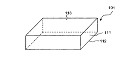
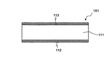
FIG. 1 is a perspective view showing a configuration of a semiconductor radiation detector according to an embodiment of the present invention, and FIG. 2 is a cross-sectional view.
本実施形態の半導体放射線検出器(以下では単に、「検出器」と称する)101は、平板状に形成された1枚の半導体結晶111と、半導体結晶111の一方の面(下面)に配置された第1電極112と、他方の面(上面)に配置された第2電極113とを備えている。
A semiconductor radiation detector (hereinafter, simply referred to as “detector”) 101 according to the present embodiment is disposed on one
半導体結晶111は、放射線(γ線等)と相互作用をして電荷を生成する領域をなしており、臭化タリウムの単結晶から切り出して形成されている。臭化タリウム単結晶は、市販の純度99.99%臭化タリウム原料を純化処理した後、単結晶育成装置によって育成する。なお、市販の純度99.99%臭化タリウム原料には、不純物として鉛(Pb)が含まれる。純化処理方法としては、帯域精製法や真空蒸留法等があるが、本実施例では、結晶中の不純物としての鉛濃度低減を目指して純化のプロセスを行った。単結晶育成方法としては、垂直ブリッジマン法を用いる。結晶の直径は約3インチである。育成した結晶の結晶格子の揺らぎの程度即ちX線回折ロッキングカーブの半値全幅は、育成時の温度勾配、成長速度、るつぼ形状、るつぼの熱伝導率等に依存するが、本実施計形態では、結晶格子の揺らぎ抑制を目指して単結晶インゴットの育成プロセスを行った。またそれと並行して、結晶格子の揺らぎの程度に着目しない育成プロセスにより、比較例の単結晶インゴットも育成した。その結果、本実施形態の単結晶インゴットNo.1と比較例の単結晶インゴットNo.2の2個の3インチ単結晶インゴットを得た。該単結晶インゴットを、インゴットを育成した時の結晶成長面に平行に内周スライサで切断した後、研磨して厚さ0.5mmの3インチ臭化タリウム単結晶ウエハを得ることができる。
The
まず、図3を用いて、本実施形態および比較例の半導体放射線検出器に用いる半導体結晶の不純物としての鉛濃度について説明する。
図3は、本発明の一実施形態による半導体放射線検出器および比較例の半導体放射線検出器に用いる半導体結晶の不純物としての鉛濃度の説明図である。
First, the lead concentration as the impurity of the semiconductor crystal used in the semiconductor radiation detectors of this embodiment and the comparative example will be described with reference to FIG.
FIG. 3 is an explanatory diagram of the concentration of lead as an impurity of a semiconductor crystal used in the semiconductor radiation detector according to one embodiment of the present invention and the semiconductor radiation detector of the comparative example.
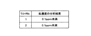
図3では、前述のNo.1とNo.2の2種類の3インチ単結晶インゴットから得た単結晶ウエハNo.1およびNo.2に含まれる不純物としての鉛の濃度を調べるため、グロー放電質量分析(GDMS:Glow Discharge Mass Spectrometry)を行った結果を示している。GDMSによる鉛濃度の検出限界は0.1ppmであるが、ウエハNo.1およびNo.2共に鉛は検出されず、鉛の濃度は共に0.1ppm未満である。 In FIG. 1 and No. No. 2 single crystal wafer No. 1 obtained from two types of 3 inch single crystal ingots. 1 and no. 2 shows the result of performing Glow Discharge Mass Spectrometry (GDMS) in order to examine the concentration of lead as an impurity contained in 2. The detection limit of lead concentration by GDMS is 0.1 ppm. 1 and no. In both cases, lead is not detected, and both lead concentrations are less than 0.1 ppm.
該単結晶ウエハを、例えば、寸法5.5mm×5.0mmにダイシングすることにより、図1及び図2に示した本実施形態の平板状体の半導体結晶111、および比較例の平板状体の半導体結晶を得る。ウエハNo.1から作製した半導体結晶111およびウエハNo.2から作製した半導体結晶共に鉛の濃度は0.1ppm未満であるので、非特許文献1に記載の放射線検出器に用いられた従来の臭化タリウム結晶に比べて鉛の濃度が低減されている。したがって、鉛原子が一部のタリウム原子を置換した置換型固溶体を作ることが少なく、結晶中の欠陥密度も小さくなっている。そのため電荷キャリアが欠陥に捕獲されることも少なく長い捕獲長を得ることができる。
The single crystal wafer is diced to a size of 5.5 mm × 5.0 mm, for example, so that the
第1電極112および第2電極113は、金または白金またはパラジウムのいずれかを用いて形成されており、その厚さは、例えば、50nmとしている。また、第1電極112および第2電極113の寸法は、例えば、5.5mm×5.0mmとしている。
The
なお、前記した半導体結晶111、第1電極112、および第2電極113の寸法は、一例を示すものであり、前記各寸法に限定されるものでない。
The dimensions of the
次に、第1電極112および第2電極113の作製工程について説明する。
Next, a manufacturing process of the
はじめに、平板状体の臭化タリウムからなる半導体結晶111の一方の面(下面、寸法5.5mm×5.0mm)に電子ビーム蒸着法によって金または白金またはパラジウムを50nm被着し、第1電極112を形成する。
First, 50 nm of gold, platinum, or palladium is deposited on one surface (lower surface, dimensions 5.5 mm × 5.0 mm) of a
次に、半導体結晶111の第1電極を形成した面と反対側の面(上面、寸法5.5mm×5.0mm)に、電子ビーム蒸着法によって金または白金またはパラジウムを50nm被着し、第2電極113を形成する。
Next, 50 nm of gold, platinum, or palladium is deposited on the surface opposite to the surface on which the first electrode of the
このような工程を経ることによって、ウエハNo.1をダイシングして得た半導体結晶111を用いて本実施形態の検出器101、またウエハNo.2をダイシングして得た半導体結晶を用いて比較例の検出器が得られる。
Through these steps, the wafer No. Using the
次に、図4を用いて、本実施形態による半導体放射線検出器を用いて放射線計測を行う場合の回路構成について説明する。
図4は、本発明の一実施形態による半導体放射線検出器を用いて放射線計測を行う場合の回路構成を示す回路図である。
Next, with reference to FIG. 4, the circuit configuration when performing radiation measurement using the semiconductor radiation detector according to the present embodiment will be described.
FIG. 4 is a circuit diagram showing a circuit configuration when radiation measurement is performed using the semiconductor radiation detector according to one embodiment of the present invention.
図4においては、検出器101に電圧を印加する平滑コンデンサ320と、平滑コンデンサ320の一方の電極に正電荷を供給する第1直流電源311と、平滑コンデンサ320の前記一方の電極に負電荷を供給する第2直流電源312とが、検出器101に接続されている。
In FIG. 4, a smoothing
さらに、第1直流電源311から平滑コンデンサ320の前記一方の電極への電流を通流するように定電流特性の極性を合わせた第1定電流ダイオード318と、平滑コンデンサ320の前記一方の電極から第2直流電源312への電流を通流するように定電流特性の極性を合わせた第2定電流ダイオード319が、第1直流電源311および第2直流電源312と検出器101との間に接続されている。
Further, the first constant
さらに、第1直流電源311と平滑コンデンサ320の前記一方の電極との間には、第1フォトモスリレー315が接続され、また、第2直流電源312と平滑コンデンサ320の前記一方の電極との間には第2フォトモスリレー316が接続されている。
Further, a
さらに、第1直流電源311と第1フォトモスリレー315との間には、保護抵抗器313が接続され、また、第2直流電源312と第2フォトモスリレー316との間には保護抵抗器314が、接続されている。保護抵抗器313、314は、過電流防止用の抵抗である。
Further, a
第1フォトモスリレー315と第2フォトモスリレー316の開閉は、スイッチ制御装置317によって制御される。
Opening and closing of the first
また、検出器101の出力にはブリーダ抵抗器321と結合コンデンサ322の一方の電極が接続され、結合コンデンサ322の他方の電極には検出器101の信号を増幅する増幅器323が接続されている。さらに、スイッチ制御装置317と増幅器323には、フォトモスリレー315、316の開閉および増幅器323の極性反転のタイミングを制御する極性統合制御装置324が接続されている。
Further, one electrode of the
第1直流電源311の負極、第2直流電源312の正極、平滑コンデンサ320の前記一方の電極以外の他方の極、およびブリーダ抵抗器321の一方の極はそれぞれ接地線に接続される。
The negative pole of the first
なお、第1定電流ダイオード318と第2定電流ダイオード319は、互いに定電流特性の極性を逆にして直列に接続されて定電流装置361を構成している。この構成において、第1定電流ダイオード318と第2定電流ダイオード319に用いられている現状の一般的な定電流ダイオードは、電界効果型トランジスタ(FET:Field Effect Transistor)のソース電極とゲート電極を短絡した構造で定電流特性が作り出されているので、逆電圧を加えた場合は電界効果型トランジスタの中で形成されているp−n接合が順方向にバイアスされ、大きな電流が流れる。つまり定電流ダイオードの電流特性は極性を持っている。したがって、第1定電流ダイオード318と第2定電流ダイオード319とは、互いに定電流特性の極性を逆にして直列に接続されることによって、極性の差がない定電流特性が得られる。
Note that the first constant
γ線等の放射線を計測する場合には、検出器101の第1電極112と第2電極113の間に、第1直流電源311あるいは第2直流電源312と平滑コンデンサ320によって、電荷収集用のバイアス電圧が印加される(例えば、+500Vあるいは−500V)。
When measuring radiation such as γ-rays, the first
ここで、検出器101の部材である半導体結晶111は臭化タリウムで構成されているので、検出器101に対して第1直流電源311を用いて例えば+500Vのバイアス電圧を連続して印加すると、半導体結晶111にポーラリゼーション(polarization)、すなわち電荷の偏りによる放射線計測性能の劣化が発生し、γ線のエネルギー分解能が劣化する。
Here, since the
ポーラリゼーションを防止するには、検出器101に印加するバイアス電圧の極性を周期的に反転する必要がある。すなわち、例えば+500Vから−500V、−500Vから+500Vに極性反転する必要がある。反転の周期は、例えば5分である。
In order to prevent polarization, it is necessary to periodically reverse the polarity of the bias voltage applied to the
最初、検出器101に+500Vのバイアス電圧を印加する場合について説明する。第1直流電源311から検出器101に対して+500Vの電圧を直接印加するとノイズが発生するため、平滑コンデンサ320を用いて検出器101に電圧を印加する。
First, a case where a bias voltage of +500 V is applied to the
スイッチ制御装置317は、検出器101に正のバイアス電圧を印加する時に第1フォトモスリレー315を閉じていると共に第2フォトモスリレー316を開いている。
The
平滑コンデンサ320は、定電流装置361を介して充電され、平滑コンデンサ320の電圧は+500Vとなる。それに伴って、検出器101に印加されるバイアス電圧も+500Vとなる。逆に、検出器101に−500Vのバイアス電圧を印加する場合、負の直流バイアス電圧は、第2直流電源312によって供給される。
The smoothing
スイッチ制御装置317は、検出器101に負のバイアス電圧を印加する時に第1フォトモスリレー315を開くと共に、第2フォトモスリレー316を閉じている。平滑コンデンサ320は、定電流装置361を介して充電され、平滑コンデンサ320の電圧は−500Vとなる。平滑コンデンサ320の一方の電極に正電荷あるいは負電荷を蓄積することで、検出器101へ印加するバイアス電圧を正負反転させる。
The
極性統合制御装置324は、5分毎の極性反転の時間情報に基づいてスイッチ制御装置317と増幅器323に「正バイアス」、「負バイアス」、「正から負へのバイアス反転」、「負から正へのバイアス反転」の指令信号を送信する。スイッチ制御装置317はこの指令信号に基づいてフォトモスリレー315、316を開閉する。
Based on the time information of polarity reversal every 5 minutes, the polarity integrated
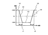
ここで、図5を用いて、本実施形態による半導体放射線検出器に印加されるバイアス電圧の時間変化について説明する。 Here, the time change of the bias voltage applied to the semiconductor radiation detector according to the present embodiment will be described with reference to FIG.
図5は、本発明の一実施形態による半導体放射線検出器に印加されるバイアス電圧の時間変化の説明図である。 FIG. 5 is an explanatory diagram of the time change of the bias voltage applied to the semiconductor radiation detector according to the embodiment of the present invention.
本実施形態において、検出器101に印加されるバイアス電圧は、最初電圧V1(+500V)であるが、バイアス電圧の周期的反転により、電圧V3(−500V)に変化し、5分後に再び電圧V5(+500V)に復帰する。
In this embodiment, the bias voltage applied to the
バイアス電圧が反転する時、その途中の電圧V2、V4の時間変化は、直線的な勾配となる。これは、定電流装置361の効果である。また、バイアス電圧を反転させる間はバイアス電圧の絶対値が電荷収集用として不十分となりγ線検出信号を十分に取出せなくなるが、計測の途切れ時間(電圧V2、V4が印加される時間t1、t2)はそれぞれ0.3秒である。5分の計測中に0.3秒の途切れ時間が発生するが、半導体放射線検出器を核医学診断装置やホームランドセキュリティに応用する場合には、十分に短い時間であって、問題とはならない。
When the bias voltage is inverted, the temporal changes in the voltages V2 and V4 along the way become a linear gradient. This is an effect of the constant
バイアス電圧が印加された検出器101にγ線が入射すると、検出器101を構成する半導体結晶111と入射したγ線との間で相互作用が起こり、電子および正孔といった電荷が生成される。
When γ rays are incident on the
生成された電荷は、検出器101からγ線検出信号として出力される。このγ線検出信号は、結合コンデンサ322を介して、増幅器323に入力される。ブリーダ抵抗器321は、結合コンデンサ322に電荷が蓄積し続けることを防止し、検出器101の出力電圧が上がり過ぎないようにする働きをする。増幅器323は、微小な電荷であるγ線検出信号を電圧に変換し増幅する働きをする。
The generated charge is output from the
増幅器323によって増幅されたγ線検出信号は、後段のアナログ・デジタル変換器(図示せず)でデジタル信号に変換され、γ線のエネルギー毎にデータ処理装置(図示せず)によってカウントされる。
The γ-ray detection signal amplified by the
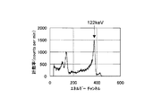
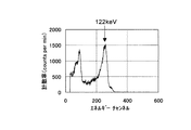
次に、図6及び図7を用いて、本実施形態および比較例による半導体放射線検出器を用いて計測した57Co線源のγ線エネルギースペクトルについて説明する。
図6及び図7は、それぞれ本発明の一実施形態による半導体放射線検出器を用いて計測したγ線エネルギースペクトルの説明図、および比較例の半導体放射線検出器を用いて計測したγ線エネルギースペクトルの説明図である。
図6は、前述のウエハNo.1から切り出した半導体結晶111を用いて検出器101を作製した場合の計測結果を示している。また、図7は、前述のウエハNo.2から切り出した半導体結晶を用いて検出器を作製した場合の計測結果を示している。
Next, the γ-ray energy spectrum of the 57 Co radiation source measured using the semiconductor radiation detector according to the present embodiment and the comparative example will be described with reference to FIGS. 6 and 7.
6 and 7 are explanatory diagrams of a γ-ray energy spectrum measured using the semiconductor radiation detector according to the embodiment of the present invention, respectively, and a γ-ray energy spectrum measured using the semiconductor radiation detector of the comparative example. It is explanatory drawing.
FIG. 6 shows the wafer No. described above. The measurement result when the
図6及び図7において、横軸はエネルギーチャンネルのチャンネル番号を示している。各番号のエネルギーチャンネルには、様々なエネルギーのγ線がエネルギー別に各チャンネルに対応づけて割り当てられている。例えば、図6において、略380チャンネル近辺のエネルギーチャンネルに対して、略122keVのγ線エネルギーが割り当てられている。縦軸は各エネルギーチャンネルのγ線の計数率(counts per min、1分当たりのカウント数)を示している。 6 and 7, the horizontal axis indicates the channel number of the energy channel. Various energy gamma rays are assigned to each energy channel in association with each energy channel. For example, in FIG. 6, approximately 122 keV of γ-ray energy is assigned to energy channels in the vicinity of approximately 380 channels. The vertical axis indicates the gamma ray count rate (counts per min, counts per minute) of each energy channel.
図6において、略122keVに対応したエネルギーチャンネルの計数率にピークが見られる。このようなピークにおけるエネルギー分解能は、次のように表わせる。 In FIG. 6, a peak is seen in the count rate of the energy channel corresponding to approximately 122 keV. The energy resolution at such a peak can be expressed as follows.
エネルギー分解能(%)=(ピークの半値幅のチャンネル数)/(ピーク直下のチャンネル数)×100 ・・・(式1)
図6に示す本実施の形態の半導体放射線検出器においては、122keVのエネルギー分解能は略5%であり、図7に示す比較例においては122keVのエネルギー分解能は略15%である。
Energy resolution (%) = (number of channels with half-width of peak) / (number of channels immediately under peak) × 100 (Equation 1)
In the semiconductor radiation detector of the present embodiment shown in FIG. 6, the energy resolution of 122 keV is about 5%, and in the comparative example shown in FIG. 7, the energy resolution of 122 keV is about 15%.
以上のように、半導体結晶の不純物としての鉛の濃度を0.1ppm未満にすることにより、本実施形態の検出器101と比較例の検出器共に122keVのγ線エネルギースペクトルを測定することが可能になる。しかしながら、本実施の形態の半導体放射線検出器と比較例とではエネルギー分解能には大きな差があり、本実施形態の検出器101において8%以下を実現できるのに対して、比較例の検出器においては8%よりも悪い値である。これは、半導体放射線検出器のエネルギー分解能が半導体結晶のX線回折ロッキングカーブに依存するという本願発明者の新たな知見に基づいて本願発明がなされたものであることによる。
As described above, by making the concentration of lead as an impurity of the semiconductor crystal less than 0.1 ppm, it is possible to measure the 122 keV γ-ray energy spectrum for both the
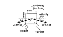
ここで、図8を用いて、本実施形態の半導体放射線検出器101に用いる半導体結晶111のX線回折ロッキングカーブの測定方法について説明する。図8は、半導体結晶111のX線回折ロッキングカーブ測定における試料配置の説明図である。
Here, a method for measuring the X-ray diffraction rocking curve of the
X線回折ロッキングカーブを測定する場合、試料結晶(TlBr結晶)にX線を入射させ、回折したX線を検出するが、回折X線の検出角度を固定し、試料の傾斜角α、回転角β、入射X線の入射角θをそれぞれ変えて3つの回折強度プロファイルを取得する。上記3つの回折強度プロファイルのそれぞれにおいて、回折強度ピークの半値全幅を、αロッキングカーブ半値幅、βロッキングカーブ半値幅、θロッキングカーブ半値幅とする。 When measuring the X-ray diffraction rocking curve, X-rays are made incident on the sample crystal (TlBr crystal) and diffracted X-rays are detected, but the detection angle of the diffracted X-rays is fixed, and the tilt angle α and rotation angle of the sample are detected. Three diffraction intensity profiles are acquired by changing the incident angle θ of incident X-rays. In each of the three diffraction intensity profiles, the full width at half maximum of the diffraction intensity peak is defined as α rocking curve half width, β rocking curve half width, and θ rocking curve half width.
次に、図9〜図12を用いて、本実施形態の半導体結晶111および比較例の半導体結晶のロッキングカーブ半値幅について説明する。図9は、本実施形態の半導体結晶111および比較例の半導体結晶の、鉛濃度、X線回折ロッキングカーブ半値幅、およびエネルギー分解能の説明図である。また図10〜図12は、それぞれ、本実施形態による検出器101および比較例の検出器に用いる半導体結晶の、試料傾斜角(α)ロッキングカーブ半値幅、試料面内回転角(β)ロッキングカーブ半値幅、X線入射角(θ)ロッキングカーブ半値幅と、検出器101および比較例の検出器の122keVエネルギー分解能の関係を示す説明図である。
Next, rocking curve half-widths of the
本実施形態の半導体結晶111として用いる3枚のウエハ、即ちNo.3〜5と、比較例の半導体結晶として用いる4枚のウエハ、即ちNo.6〜9、計7枚のウエハについて、鉛濃度と、結晶格子の揺らぎの程度即ちX線回折ロッキングカーブ半値幅と、122keVエネルギー分解能を評価した。上記7枚のウエハの原料については、結晶中の不純物としての鉛濃度低減を目指して純化のプロセスを行い、上記7枚のウエハのGDMSによる鉛の濃度は全て0.1ppm未満であった。試料傾斜角スキャンにおけるαロッキングカーブ半値幅が1.6deg以下、かつ試料面内回転角スキャンにおけるβロッキングカーブ半値幅が3.5deg以下、かつX線入射角スキャンにおけるθロッキングカーブ半値幅が1.3deg以下である3つの測定点が本実施形態のウエハNo.3〜5の測定結果であり、その他の4つの測定点が比較例のウエハNo.6〜9の測定結果である。本実施の形態における半導体結晶のように、鉛濃度が0.1ppm未満で、かつαロッキングカーブ半値幅が1.6deg以下、かつβロッキングカーブ半値幅が3.5deg以下、かつθロッキングカーブ半値幅が1.3deg以下であれば、8%以下の122keVエネルギー分解能を得られることがわかる。
Three wafers used as the
次に、13を用いて、本実施形態の半導体放射線検出器101を用いて計測した137Cs線源のγ線エネルギースペクトルについて説明する。
図13は、前述のインゴットNo.1から得たウエハNo.1から切り出した半導体結晶111を用いて検出器101を作製した場合の計測結果を示している。
図13において、横軸はエネルギーチャンネルのチャンネル番号を示している。縦軸は各エネルギーチャンネルのγ線の計数率(counts per min、1分当たりのカウント数)である。
Next, the γ-ray energy spectrum of the 137 Cs radiation source measured using the
FIG. 13 shows the ingot No. described above. No. 1 obtained from wafer No. 1 The measurement result when the
In FIG. 13, the horizontal axis indicates the channel number of the energy channel. The vertical axis represents the gamma ray count rate (counts per min, counts per minute) of each energy channel.
図13においては662keVのエネルギー分解能は略4%である。 In FIG. 13, the energy resolution of 662 keV is approximately 4%.
以上、図1に示した本実施形態の検出器101を、ウエハNo.1から切出した半導体結晶111を用いて構成することにより、高いエネルギー分解能で662keVのエネルギースペクトルが得られる。
As described above, the
したがって、本実施形態の検出器101は、122keVおよび662keVの放射線計測性能の点で、非特許文献1に記載の従来の臭化タリウム結晶を半導体結晶に用いて検出器を構成した場合に比べて、大きく改善され、122keVで8%以下のエネルギー分解能を得られ、662keVにおいても高いエネルギー分解能を得られている。これは、本実施形態の検出器101において、半導体結晶111を、鉛の濃度が0.1ppm未満であり、かつX線回折における(110)ロッキングカーブの、試料傾斜角スキャンにおける半値全幅が1.6deg以下、試料面内回転角スキャンにおける半値全幅が3.5deg以下、X線入射角スキャンにおける半値全幅が1.3deg以下である臭化タリウムの単結晶で構成したことによる。
Therefore, the
半導体結晶として、鉛の濃度が0.1ppm未満である臭化タリウムの単結晶を用いることで、臭化タリウム単結晶中の鉛原子の濃度が小さいので、タリウム原子に対して鉛原子が置換してできる結晶中の欠陥の密度が小さくなり、電荷キャリアの捕獲長を長くできるので、放射線検出器として、122keVおよび662keVのγ線エネルギースペクトルを計測することができる。 By using a single crystal of thallium bromide with a lead concentration of less than 0.1 ppm as the semiconductor crystal, the concentration of lead atoms in the thallium bromide single crystal is small, so that lead atoms are substituted for thallium atoms. As a result, the density of defects in the resulting crystal is reduced and the charge carrier capture length can be increased, so that 122 gV and 662 keV γ-ray energy spectra can be measured as a radiation detector.
ここで、半導体結晶として、鉛の濃度が0.1ppm未満である臭化タリウムの単結晶を用いるということは、鉛の濃度がグロー放電質量分析(GDMS:Glow Discharge Mass Spectrometry)における鉛の検出限界以下である臭化タリウムの単結晶を用いるということもできるものである。このような半導体結晶を用いることで、放射線検出器として、122keVおよび662keVのγ線エネルギースペクトルを計測することができる。 Here, as a semiconductor crystal, a single crystal of thallium bromide having a lead concentration of less than 0.1 ppm means that the lead concentration is the detection limit of lead in Glow Discharge Mass Spectrometry (GDMS). It can also be said that the following single crystal of thallium bromide is used. By using such a semiconductor crystal, it is possible to measure 122 keV and 662 keV γ-ray energy spectra as a radiation detector.
また、半導体結晶として、鉛の濃度が0.1ppm未満である臭化タリウムの単結晶を用いるということは、半導体結晶として、鉛の濃度が0.0ppmである臭化タリウムの単結晶を用いるということもできる。ここで、鉛の濃度が0.0ppmであるということは、有効数字2桁以下の桁の数字は何でもよく、例えば、0.099ppm、0.09ppm、0.04ppm、や0.01ppm以下の鉛濃度を含むものである。このような半導体結晶を用いることで、放射線検出器として、122keVおよび662keVのγ線エネルギースペクトルを計測することができる。 In addition, using a thallium bromide single crystal having a lead concentration of less than 0.1 ppm as a semiconductor crystal means using a thallium bromide single crystal having a lead concentration of 0.0 ppm as the semiconductor crystal. You can also. Here, the lead concentration of 0.0 ppm means that the number of digits with two or less significant digits is not limited, for example, lead of 0.099 ppm, 0.09 ppm, 0.04 ppm, or 0.01 ppm or less. Includes concentration. By using such a semiconductor crystal, it is possible to measure 122 keV and 662 keV γ-ray energy spectra as a radiation detector.
さらに、半導体結晶として、鉛の濃度が0.1ppm未満である臭化タリウムの単結晶を用いるということは、半導体結晶として、鉛の置換型固溶体を含まない臭化タリウムの単結晶を用いるということもできる。これは、鉛の濃度が0.1ppm未満と低い場合、不純物の鉛によってタリウム原子の一部が置換されて置換型固溶体が形成されることがなく、欠陥が生じないため、電荷キャリアが捕獲されにくく捕獲長が長くなる。そのため、このような半導体結晶を用いることで、放射線検出器として、122keVおよび662keVのγ線エネルギースペクトルを計測することができる。 Furthermore, using a single crystal of thallium bromide with a lead concentration of less than 0.1 ppm as a semiconductor crystal means that a single crystal of thallium bromide that does not contain a lead substitutional solid solution is used as the semiconductor crystal. You can also. This is because, when the lead concentration is as low as less than 0.1 ppm, some of the thallium atoms are not substituted by the lead impurity, so that a substitutional solid solution is not formed and defects are not generated, so that charge carriers are captured. Difficult to capture long. Therefore, by using such a semiconductor crystal, 122 keV and 662 keV γ-ray energy spectra can be measured as a radiation detector.
さらに、半導体結晶として、鉛の濃度が0.1ppm未満である臭化タリウムの単結晶を用いるということは、半導体結晶として、電荷キャリアが捕獲される欠陥がない臭化タリウムの単結晶を用いるということもできる。これは、鉛の濃度が0.1ppm未満と低い場合、不純物の鉛によってタリウム原子の一部が置換されて置換型固溶体が形成されることがなく、電荷キャリアを捕獲する欠陥が生じないため、電荷キャリアが捕獲されにくく捕獲長が長くなる。そのため、このような半導体結晶を用いることで、放射線検出器として、122keVおよび662keVのγ線エネルギースペクトルを計測することができる。 Furthermore, the use of a single crystal of thallium bromide having a lead concentration of less than 0.1 ppm as the semiconductor crystal means that a single crystal of thallium bromide having no defects in which charge carriers are trapped is used as the semiconductor crystal. You can also. This is because when the lead concentration is as low as less than 0.1 ppm, a part of the thallium atom is not substituted by the lead impurity, so that a substitutional solid solution is not formed, and defects that trap charge carriers do not occur. Charge carriers are not easily captured and the capture length is increased. Therefore, by using such a semiconductor crystal, 122 keV and 662 keV γ-ray energy spectra can be measured as a radiation detector.
また、半導体結晶として、X線回折における(110)ロッキングカーブの、試料傾斜角スキャンにおける半値全幅が1.6deg以下、試料面内回転角スキャンにおける半値全幅が3.5deg以下、X線入射角スキャンにおける半値全幅が1.3deg以下である臭化タリウムの単結晶を用いることで、単結晶中の結晶格子の揺らぎを小さくできるので、電荷キャリアの移動度と寿命の積を大きくできる。これにより、放射線検出器として、さらに高いエネルギー分解能すなわち8%以下のエネルギー分解能で122keVのγ線エネルギースペクトルを計測することができる。 Further, as a semiconductor crystal, the full width at half maximum in the sample tilt angle scan of the (110) rocking curve in X-ray diffraction is 1.6 degs or less, the full width at half maximum in the in-plane rotation angle scan is 3.5 degs or less, and the X-ray incident angle scan. By using a single crystal of thallium bromide having a full width at half maximum of 1.3 deg or less, fluctuations of the crystal lattice in the single crystal can be reduced, so that the product of charge carrier mobility and lifetime can be increased. Thereby, as a radiation detector, a 122 keV γ-ray energy spectrum can be measured with a higher energy resolution, that is, an energy resolution of 8% or less.
次に、図14及び図15を用いて、本実施形態による半導体放射線検出器を用いた核医学診断装置の構成について説明する。
図14及び図15は、本発明の一実施形態による半導体放射線検出器を用いた核医学診断装置の構成図である。
Next, the configuration of the nuclear medicine diagnostic apparatus using the semiconductor radiation detector according to the present embodiment will be described with reference to FIGS. 14 and 15.
14 and 15 are configuration diagrams of a nuclear medicine diagnostic apparatus using a semiconductor radiation detector according to an embodiment of the present invention.
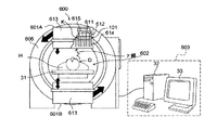
最初に、図14を用いて、核医学診断装置として、単光子放射断層撮像装置(SPECT撮像装置)600に本実施形態の検出器101を適用した場合について説明する。
First, the case where the
図14において、SPECT撮像装置600は、中央部分に円柱状の計測領域602を取り囲むようにして、2台の上下に位置した放射線検出ブロック601A、601Bと、回転支持台606と、ベッド31と、画像情報作成装置603を備えている。
In FIG. 14, a
ここで、上側に位置する放射線検出ブロック601Aは、複数の放射線計測ユニット611と、ユニット支持部材615と、遮光・電磁シールド613とを備えている。放射線計測ユニット611は、複数の半導体放射線検出器101と、基板612と、コリメータ614とを備えている。また、下部に位置する放射線検出ブロック601Bも同様の構成である。また、画像情報作成装置603は、データ処理装置32と、表示装置33とから構成されている。
Here, the
放射線検出ブロック601A、601Bは、回転支持台606において周方向に180度ずれた位置に配置されている。具体的には、それぞれの放射線検出ブロック601A、601Bの各ユニット支持部材615(一方のみ図示)が、周方向に180度隔てた位置で回転支持台606に取り付けられる。そして、ユニット支持部材615に、基板612を含む複数の放射線計測ユニット611が着脱可能に取り付けられている。
The radiation detection blocks 601 </ b> A and 601 </ b> B are arranged at positions shifted by 180 degrees in the circumferential direction on the
複数の検出器101は、コリメータ614で仕切られる領域Kに、基板612に取り付けられた状態で多段にそれぞれ配置される。コリメータ614は、放射線遮蔽材(例えば、鉛、タングステン等)から形成され、放射線(例えば、γ線)が通過する多数の放射線通路を形成している。
The plurality of
全ての基板612およびコリメータ614は、回転支持台606に設置された遮光・電磁シールド613内に配置される。この遮光・電磁シールド613は、γ線以外の電磁波の検出器101等への影響を遮断している。
All the
このようなSPECT撮像装置600では、放射性薬剤を投与された被検体Hが載置されるベッド31が移動され、被検体Hは、一対の放射線検出ブロック601A、601Bの間に移動される。そして、回転支持台606が回転されることによって、各放射線検出ブロック601A、601Bが被検体Hの周囲を旋回して検出が開始される。
In such a
そして、放射性薬剤が集積した被検体H内の集積部(例えば、患部)Dからγ線が放出されると、放出されたγ線がコリメータ614の放射線通路を通って対応する検出器101に入射する。そして、検出器101は、γ線検出信号を出力する。このγ線検出信号は、γ線のエネルギー毎にデータ処理装置32によってカウントされ、その情報等が表示装置33に表示される。
When γ-rays are emitted from the accumulation part (for example, affected part) D in the subject H where the radiopharmaceutical is accumulated, the emitted γ-rays enter the
なお、図14において、放射線検出ブロック601A、601Bは、回転支持台606に支えられながら、太い矢印で示したように回転し、被検体Hとの角度を変えながら、撮像、および計測を行う。また、放射線検出ブロック601A、601Bは、細い矢印で示したように上下に移動可能であり、被検体Hとの距離を変えることができる。
In FIG. 14, the radiation detection blocks 601 </ b> A and 601 </ b> B rotate as indicated by thick arrows while being supported by the
このようなSPECT撮像装置600に用いられた検出器101は、半導体結晶として臭化タリウムを用いつつ、8%以下の高いエネルギー分解能で122keVのγ線エネルギースペクトルを計測可能である。したがって、小型で安価、かつ核医学検査用の放射性医薬品に用いられる代表的な放射性核種であり141keVのγ線を放出する99mTc、および159keVのγ線を放出する123Iを高いエネルギー分解能で二核種同時撮像可能なSPECT撮像装置を提供することが可能になる。
The
次に、図15を用いて、核医学診断装置として、PET撮像装置700に本実施形態の検出器101を適用した場合について説明する。
Next, the case where the
本実施形態の検出器101は、SPECT撮像装置600に限られることではなく、核医学診断装置としての、ガンマカメラ装置、PET撮像装置等に対しても用いることができる。
The
図15において、陽電子放出型断層撮像装置(PET撮像装置)700は、中央部分に円柱状の計測領域702を有する撮像装置701と、被検体Hを支持して長手方向に移動可能なベッド31と、画像情報作成装置703を備えて構成される。なお、画像情報作成装置703は、データ処理装置32および表示装置33を備えて構成されている。
In FIG. 15, a positron emission tomographic imaging apparatus (PET imaging apparatus) 700 includes an
撮像装置701には、計測領域702を取り囲むようにして、前記検出器101を多数搭載した基板Pが配置されている。
In the
このようなPET撮像装置700では、データ処理機能を有するデジタルASIC(デジタル回路用のApplication Specific Integrated Circuit、デジタル回路用の特定用途向け集積回路、図示せず)等を備え、γ線のエネルギー値、時刻、検出器101の検出チャンネルID(Identification)を有するパケットが作成され、この作成されたパケットがデータ処理装置32に入力されるようになっている。
Such a
検査時には、被検体Hの体内から放射性薬剤に起因して放射されたγ線が、検出器101によって検出される。すなわち、PET撮像用の放射性薬剤から放出された陽電子の消滅時に、一対のγ線が約180度の反対方向に放出され、多数の検出器101のうち別々の検出チャンネルで検出される。検出されたγ線検出信号は、該当する前記デジタルASICに入力されて、前記したように信号処理が行われ、γ線を検出した検出チャンネルの位置情報およびγ線の検出時刻情報が、データ処理装置32に入力される。
At the time of examination, the
そして、データ処理装置32によって、1つの陽電子の消滅により発生した一対のγ線を1個として計数(同時計数)し、その一対のγ線を検出した2つの検出チャンネルの位置を、それらの位置情報を基に特定する。また、データ処理装置32は、同時計数で得た計数値および検出チャンネルの位置情報を用いて、放射性薬剤の集積位置、すなわち腫瘍位置での被検体Hの断層像情報(画像情報)を作成する。この断層像情報は表示装置33に表示される。
Then, the
このようなPET撮像装置700に用いられた検出器101は、半導体結晶として臭化タリウムを用いつつ、高いエネルギー分解能で662keVのγ線エネルギースペクトルを計測可能である。したがって、小型で安価、かつPET検査用の放射性医薬品から発生した陽電子より放出される511keVのγ線を高いエネルギー分解能で検出可能なPET撮像装置を提供することが可能になる。
The
以上説明したように、本実施形態によれば、放射線検出器を構成する半導体結晶として臭化タリウムを用いつつ、該放射線検出器によって高いエネルギー分解能で122keVおよび662keVのγ線エネルギースペクトルを計測可能である。したがって、小型で安価、かつエネルギー分解能が高い半導体放射線検出器、およびこの半導体放射線検出器を搭載した核医学診断装置を提供できる。 As described above, according to the present embodiment, while using thallium bromide as a semiconductor crystal constituting the radiation detector, it is possible to measure 122 keV and 662 keV γ-ray energy spectra with high energy resolution by the radiation detector. is there. Therefore, it is possible to provide a semiconductor radiation detector that is small, inexpensive, and has high energy resolution, and a nuclear medicine diagnostic apparatus equipped with this semiconductor radiation detector.
なお、本発明の半導体放射線検出器、およびそれを搭載した核医学診断装置は、高いエネルギー分解能で放射性薬剤を撮像可能であり、かつ小型化および価格低減を図ることができるため、これら装置の普及に貢献して、この分野で広く利用、採用される。 The semiconductor radiation detector of the present invention and the nuclear medicine diagnostic apparatus equipped with the semiconductor radiation detector are capable of imaging radiopharmaceuticals with high energy resolution, and can be downsized and reduced in price. Widely used and adopted in this field.
31…ベッド
32…データ処理装置
33…表示装置
101…半導体放射線検出器(検出器)
111…半導体結晶
112…第1電極
113…第2電極
311…第1直流電源
312…第2直流電源
313、314…保護抵抗器
315…第1フォトモスリレー
316…第2フォトモスリレー
317…スイッチ制御装置
318…第1定電流ダイオード
319…第2定電流ダイオード
320…平滑コンデンサ
321…ブリーダ抵抗器
322…結合コンデンサ
323…増幅器
324…極性統合制御装置
361…定電流装置
600…SPECT撮像装置
601A、601B…放射線検出ブロック
602、702…計測領域
603、703…画像情報作成装置
606…回転支持台
611…放射線計測ユニット
612…基板
613…遮光・電磁シールド
614…コリメータ
615…ユニット支持部材
700…PET撮像装置
701…撮像装置
D…集積部
H…被検体
K…コリメータで仕切られる領域
P…基板
31 ...
DESCRIPTION OF
Claims (9)
前記半導体結晶は、不純物としての鉛の濃度が0.1ppm未満であり、かつX線回折における(110)ロッキングカーブの、試料傾斜角スキャンにおける半値全幅が1.6deg以下、試料面内回転角スキャンにおける半値全幅が3.5deg以下、X線入射角スキャンにおける半値全幅が1.3deg以下である臭化タリウムの単結晶で構成されていることを特徴とする半導体放射線検出器。 A semiconductor radiation detector using a semiconductor crystal sandwiched between a cathode electrode and an anode electrode,
The semiconductor crystal has a concentration of lead as an impurity of less than 0.1 ppm, a full width at half maximum in a sample tilt angle scan of a (110) rocking curve in X-ray diffraction is 1.6 degs or less, and a sample in-plane rotation angle scan A semiconductor radiation detector, comprising a single crystal of thallium bromide having a full width at half maximum of 3.5 degs or less and a full width at half maximum in an X-ray incident angle scan of 1.3 degs or less.
前記半導体結晶は、不純物としての鉛の濃度がグロー放電質量分析(GDMS)による鉛濃度の検出限界以下であり、かつX線回折における(110)ロッキングカーブの、試料傾斜角スキャンにおける半値全幅が1.6deg以下、試料面内回転角スキャンにおける半値全幅が3.5deg以下、X線入射角スキャンにおける半値全幅が1.3deg以下である臭化タリウムの単結晶で構成されていることを特徴とする半導体放射線検出器。 A semiconductor radiation detector using a semiconductor crystal sandwiched between a cathode electrode and an anode electrode,
In the semiconductor crystal, the concentration of lead as an impurity is less than the detection limit of lead concentration by glow discharge mass spectrometry (GDMS), and the full width at half maximum in the sample inclination scan of the (110) rocking curve in X-ray diffraction is 1 .6 deg or less, the full width at half maximum in the in-plane rotation angle scan is 3.5 degs or less, and the full width at half maximum in the X-ray incident angle scan is 1.3 degs or less. Semiconductor radiation detector.
前記半導体結晶は、不純物としての鉛の濃度が0.0ppmであり、かつX線回折における(110)ロッキングカーブの、試料傾斜角スキャンにおける半値全幅が1.6deg以下、試料面内回転角スキャンにおける半値全幅が3.5deg以下、X線入射角スキャンにおける半値全幅が1.3deg以下である臭化タリウムの単結晶で構成されていることを特徴とする半導体放射線検出器。 A semiconductor radiation detector using a semiconductor crystal sandwiched between a cathode electrode and an anode electrode,
In the semiconductor crystal, the concentration of lead as an impurity is 0.0 ppm, the full width at half maximum in the sample inclination angle scan of the (110) rocking curve in X-ray diffraction is 1.6 degs or less, and in the in-plane rotation angle scan A semiconductor radiation detector comprising a single crystal of thallium bromide having a full width at half maximum of 3.5 degs or less and a full width at half maximum in an X-ray incident angle scan of 1.3 degs or less.
前記カソード電極および前記アノード電極を金、白金、パラジウムのうちの少なくとも一つ以上の金属で構成したことを特徴とする半導体放射線検出器 The semiconductor radiation detector according to any one of claims 1 to 3,
A semiconductor radiation detector comprising the cathode electrode and the anode electrode made of at least one metal selected from gold, platinum and palladium.
前記半導体結晶として、不純物としての鉛の濃度が0.1ppm未満であり、かつX線回折における(110)ロッキングカーブの、試料傾斜角スキャンにおける半値全幅が1.6deg以下、試料面内回転角スキャンにおける半値全幅が3.5deg以下、X線入射角スキャンにおける半値全幅が1.3deg以下である臭化タリウムの単結晶を選択することを特徴とする半導体放射線検出器の製造方法。 A method of manufacturing a semiconductor detector using a semiconductor crystal sandwiched between a cathode electrode and an anode electrode,
As the semiconductor crystal, the concentration of lead as an impurity is less than 0.1 ppm, the full width at half maximum in the sample inclination angle scan of the (110) rocking curve in X-ray diffraction is 1.6 degs or less, and the sample in-plane rotation angle scan A method for producing a semiconductor radiation detector, comprising selecting a thallium bromide single crystal having a full width at half maximum of 3.5 degs or less and a full width at half maximum in an X-ray incident angle scan of 1.3 degs or less.
前記半導体結晶として、不純物としての鉛の濃度がグロー放電質量分析(GDMS)による鉛濃度の検出限界以下であり、かつX線回折における(110)ロッキングカーブの、試料傾斜角スキャンにおける半値全幅が1.6deg以下、試料面内回転角スキャンにおける半値全幅が3.5deg以下、X線入射角スキャンにおける半値全幅が1.3deg以下である臭化タリウムの単結晶を選択することを特徴とする半導体放射線検出器の製造方法。 A method of manufacturing a semiconductor detector using a semiconductor crystal sandwiched between a cathode electrode and an anode electrode,
As the semiconductor crystal, the concentration of lead as an impurity is less than the detection limit of lead concentration by glow discharge mass spectrometry (GDMS), and the full width at half maximum in the sample inclination scan of the (110) rocking curve in X-ray diffraction is 1. A semiconductor radiation characterized by selecting a single crystal of thallium bromide having a .6 deeg or less, a full width at half maximum in an in-plane rotation angle scan of 3.5 degs or less, and a full width at half maximum in an X-ray incident angle scan of 1.3 degs or less. Manufacturing method of the detector.
前記半導体結晶として、不純物としての鉛の濃度が0.0ppmであり、かつX線回折における(110)ロッキングカーブの、試料傾斜角スキャンにおける半値全幅が1.6deg以下、試料面内回転角スキャンにおける半値全幅が3.5deg以下、X線入射角スキャンにおける半値全幅が1.3deg以下である臭化タリウムの単結晶を選択することを特徴とする半導体放射線検出器の製造方法。 A method of manufacturing a semiconductor detector using a semiconductor crystal sandwiched between a cathode electrode and an anode electrode,
As the semiconductor crystal, the concentration of lead as an impurity is 0.0 ppm, and the full width at half maximum in the sample tilt angle scan of the (110) rocking curve in X-ray diffraction is 1.6 degs or less. A method for manufacturing a semiconductor radiation detector, comprising selecting a single crystal of thallium bromide having a full width at half maximum of 3.5 degs or less and a full width at half maximum in an X-ray incident angle scan of 1.3 degs or less.
前記半導体結晶を作製する場合に、前記半導体結晶の原材料となるインゴットを育成した時の結晶成長面に平行に切断してカソード電極およびアノード電極を被着する面を形成することを特徴とする半導体放射線検出器の製造方法。 A method for manufacturing a semiconductor radiation detector according to any one of claims 5 to 7,
When producing the semiconductor crystal, a semiconductor is characterized in that a surface on which a cathode electrode and an anode electrode are deposited is formed by cutting in parallel to a crystal growth surface when an ingot as a raw material of the semiconductor crystal is grown. A method for manufacturing a radiation detector.
前記基板の前記複数の半導体放射線検出器から出力された放射線検出信号を基に得られた情報を用いて画像を生成する画像情報作成装置とを備え、
前記半導体放射線検出器が、請求項1〜3の何れか1項に記載の半導体放射線検出器であることを特徴とする核医学診断装置。 A plurality of the semiconductor radiation detectors are attached, surround a measurement region where a bed supporting a subject is inserted, and a substrate disposed around the measurement region;
An image information creation device that generates an image using information obtained based on radiation detection signals output from the plurality of semiconductor radiation detectors of the substrate;
The nuclear medicine diagnostic apparatus, wherein the semiconductor radiation detector is the semiconductor radiation detector according to any one of claims 1 to 3.
Priority Applications (5)
| Application Number | Priority Date | Filing Date | Title |
|---|---|---|---|
| JP2013208107A JP2015072201A (en) | 2013-10-03 | 2013-10-03 | Semiconductor radiation detector, nuclear medicine diagnostic device using semiconductor radiation detector, and semiconductor radiation detector manufacturing method |
| US15/025,580 US20160206257A1 (en) | 2013-10-03 | 2014-09-30 | Semiconductor radiation detector, nuclear medicine diagnostic device using that detector, and manufacturing method of semiconductor radiation detector |
| PCT/JP2014/076195 WO2015050141A1 (en) | 2013-10-03 | 2014-09-30 | Semiconductor radiation detector, nuclear medicine diagnostic device using same, and method for producing semiconductor radiation detector |
| CN201480052242.3A CN105579868A (en) | 2013-10-03 | 2014-09-30 | Semiconductor radiation detector, nuclear medicine diagnostic device using same, and method for producing semiconductor radiation detector |
| EP14851321.1A EP3054321A4 (en) | 2013-10-03 | 2014-09-30 | Semiconductor radiation detector, nuclear medicine diagnostic device using same, and method for producing semiconductor radiation detector |
Applications Claiming Priority (1)
| Application Number | Priority Date | Filing Date | Title |
|---|---|---|---|
| JP2013208107A JP2015072201A (en) | 2013-10-03 | 2013-10-03 | Semiconductor radiation detector, nuclear medicine diagnostic device using semiconductor radiation detector, and semiconductor radiation detector manufacturing method |
Publications (2)
| Publication Number | Publication Date |
|---|---|
| JP2015072201A true JP2015072201A (en) | 2015-04-16 |
| JP2015072201A5 JP2015072201A5 (en) | 2016-06-23 |
Family
ID=52778729
Family Applications (1)
| Application Number | Title | Priority Date | Filing Date |
|---|---|---|---|
| JP2013208107A Pending JP2015072201A (en) | 2013-10-03 | 2013-10-03 | Semiconductor radiation detector, nuclear medicine diagnostic device using semiconductor radiation detector, and semiconductor radiation detector manufacturing method |
Country Status (5)
| Country | Link |
|---|---|
| US (1) | US20160206257A1 (en) |
| EP (1) | EP3054321A4 (en) |
| JP (1) | JP2015072201A (en) |
| CN (1) | CN105579868A (en) |
| WO (1) | WO2015050141A1 (en) |
Cited By (5)
| Publication number | Priority date | Publication date | Assignee | Title |
|---|---|---|---|---|
| CN108763758A (en) * | 2018-05-29 | 2018-11-06 | 南京航空航天大学 | A kind of GATE emulation modes of non-complete ring-type PET rotation sweep patterns |
| WO2020100467A1 (en) * | 2018-11-12 | 2020-05-22 | 浜松ホトニクス株式会社 | Radiation detector and method for producing same |
| JP2020115150A (en) * | 2020-04-06 | 2020-07-30 | 浜松ホトニクス株式会社 | Method for manufacturing radiation detector |
| JP2021006832A (en) * | 2018-10-31 | 2021-01-21 | 浜松ホトニクス株式会社 | Manufacturing method of radiation detector |
| US11307315B2 (en) | 2016-07-11 | 2022-04-19 | Hamamatsu Photonics K.K. | Radiation detector |
Families Citing this family (3)
| Publication number | Priority date | Publication date | Assignee | Title |
|---|---|---|---|---|
| CN105759304B (en) * | 2016-04-22 | 2018-08-14 | 西北核技术研究所 | A kind of X-ray energy spectrum measurement method based on optical flat diffraction imaging |
| WO2019084703A1 (en) * | 2017-10-30 | 2019-05-09 | Shenzhen Xpectvision Technology Co., Ltd. | Radiation detector with dc-to-dc converter based on mems switches |
| CN108345026B (en) * | 2018-02-09 | 2021-06-15 | 哈尔滨工业大学 | Method for calculating energy spectrum of charged particle after protective layer |
Citations (7)
| Publication number | Priority date | Publication date | Assignee | Title |
|---|---|---|---|---|
| JP2005223009A (en) * | 2004-02-03 | 2005-08-18 | Hitachi Ltd | Semiconductor radiation detector and radiation detecting device |
| WO2009022378A1 (en) * | 2007-08-10 | 2009-02-19 | Osaka Electro-Communication University | Radiation detector |
| JP2011185803A (en) * | 2010-03-10 | 2011-09-22 | Hitachi Ltd | Radiation measuring apparatus and nuclear medicine diagnostic equipment |
| JP2012167938A (en) * | 2011-02-10 | 2012-09-06 | Hitachi Ltd | Radiation measuring device and nuclear medicine diagnostic apparatus using the same |
| US20130126746A1 (en) * | 2010-05-03 | 2013-05-23 | Brookhaven Science Associates, Llc | Array of virtual frisch-grid detectors with common cathode and reduced length of shielding electrodes |
| JP2013156048A (en) * | 2012-01-27 | 2013-08-15 | Hitachi Ltd | Semiconductor radiation detector and nuclear medicine diagnosis device |
| JP2013157494A (en) * | 2012-01-31 | 2013-08-15 | Jx Nippon Mining & Metals Corp | Radiation detecting element, radiation detector and radiation detecting element manufacturing method |
Family Cites Families (4)
| Publication number | Priority date | Publication date | Assignee | Title |
|---|---|---|---|---|
| JP2001349948A (en) * | 2000-06-08 | 2001-12-21 | Nec Corp | X-ray light emitting element |
| JP3863873B2 (en) * | 2003-09-30 | 2006-12-27 | 株式会社日立製作所 | Radiation inspection equipment |
| JP2009286856A (en) * | 2008-05-27 | 2009-12-10 | Fukuda Crystal Laboratory | Scintillator material, method for manufacturing the same, and ionizing radiation detector |
| CN102471921B (en) * | 2009-07-23 | 2016-05-25 | 住友电气工业株式会社 | For the manufacture of method and apparatus and the semiconductor crystal of semiconductor crystal |
-
2013
- 2013-10-03 JP JP2013208107A patent/JP2015072201A/en active Pending
-
2014
- 2014-09-30 CN CN201480052242.3A patent/CN105579868A/en active Pending
- 2014-09-30 WO PCT/JP2014/076195 patent/WO2015050141A1/en active Application Filing
- 2014-09-30 EP EP14851321.1A patent/EP3054321A4/en not_active Withdrawn
- 2014-09-30 US US15/025,580 patent/US20160206257A1/en not_active Abandoned
Patent Citations (7)
| Publication number | Priority date | Publication date | Assignee | Title |
|---|---|---|---|---|
| JP2005223009A (en) * | 2004-02-03 | 2005-08-18 | Hitachi Ltd | Semiconductor radiation detector and radiation detecting device |
| WO2009022378A1 (en) * | 2007-08-10 | 2009-02-19 | Osaka Electro-Communication University | Radiation detector |
| JP2011185803A (en) * | 2010-03-10 | 2011-09-22 | Hitachi Ltd | Radiation measuring apparatus and nuclear medicine diagnostic equipment |
| US20130126746A1 (en) * | 2010-05-03 | 2013-05-23 | Brookhaven Science Associates, Llc | Array of virtual frisch-grid detectors with common cathode and reduced length of shielding electrodes |
| JP2012167938A (en) * | 2011-02-10 | 2012-09-06 | Hitachi Ltd | Radiation measuring device and nuclear medicine diagnostic apparatus using the same |
| JP2013156048A (en) * | 2012-01-27 | 2013-08-15 | Hitachi Ltd | Semiconductor radiation detector and nuclear medicine diagnosis device |
| JP2013157494A (en) * | 2012-01-31 | 2013-08-15 | Jx Nippon Mining & Metals Corp | Radiation detecting element, radiation detector and radiation detecting element manufacturing method |
Non-Patent Citations (3)
| Title |
|---|
| DONGXIANG ZHOU ET AL.: "A Novel Method to Grow Thallium Bromide Single Crystal and Crystal", CRYSTAL GROWTH & DESIGN, vol. Vol. 9, No. 10, 2009, JPN7017002814, 15 September 2009 (2009-09-15), US, pages 4296 - 4300, ISSN: 0003750109 * |
| V.KOZLOV ET AL.: "Annealing and characterisation of TlBr crystals", NUCLEAR INSTRUMENTS AND METHODS IN PHYSICS RESEARCH, vol. A 546(2005), JPN6017032587, 7 April 2005 (2005-04-07), US, pages 200 - 204, ISSN: 0003750108 * |
| V.KOZLOV ET AL.: "TlBr crystal growth, purification and characterisation", NUCLEAR INSTRUMENTS AND METHODS IN PHYSICS RESEARCH, vol. A 531(2004), JPN6017032585, 22 June 2004 (2004-06-22), US, pages 165 - 173, ISSN: 0003750107 * |
Cited By (8)
| Publication number | Priority date | Publication date | Assignee | Title |
|---|---|---|---|---|
| US11307315B2 (en) | 2016-07-11 | 2022-04-19 | Hamamatsu Photonics K.K. | Radiation detector |
| US11555934B2 (en) | 2016-07-11 | 2023-01-17 | Hamamatsu Photonics K.K. | Radiation detector |
| CN108763758A (en) * | 2018-05-29 | 2018-11-06 | 南京航空航天大学 | A kind of GATE emulation modes of non-complete ring-type PET rotation sweep patterns |
| CN108763758B (en) * | 2018-05-29 | 2022-05-03 | 南京航空航天大学 | GATE simulation method of incomplete annular PET (positron emission tomography) rotary scanning mode |
| JP2021006832A (en) * | 2018-10-31 | 2021-01-21 | 浜松ホトニクス株式会社 | Manufacturing method of radiation detector |
| WO2020100467A1 (en) * | 2018-11-12 | 2020-05-22 | 浜松ホトニクス株式会社 | Radiation detector and method for producing same |
| JP2020115150A (en) * | 2020-04-06 | 2020-07-30 | 浜松ホトニクス株式会社 | Method for manufacturing radiation detector |
| JP7051928B2 (en) | 2020-04-06 | 2022-04-11 | 浜松ホトニクス株式会社 | How to manufacture a radiation detector |
Also Published As
| Publication number | Publication date |
|---|---|
| EP3054321A4 (en) | 2017-05-31 |
| EP3054321A1 (en) | 2016-08-10 |
| WO2015050141A1 (en) | 2015-04-09 |
| US20160206257A1 (en) | 2016-07-21 |
| CN105579868A (en) | 2016-05-11 |
Similar Documents
| Publication | Publication Date | Title |
|---|---|---|
| JP6049166B2 (en) | Semiconductor radiation detector and nuclear medicine diagnostic apparatus using the same | |
| WO2015050141A1 (en) | Semiconductor radiation detector, nuclear medicine diagnostic device using same, and method for producing semiconductor radiation detector | |
| US8816292B2 (en) | Compact endocavity diagnostic probes for nuclear radiation detection | |
| Churilov et al. | Thallium bromide nuclear radiation detector development | |
| JP5753802B2 (en) | Semiconductor radiation detector and nuclear medicine diagnostic equipment | |
| Hitomi et al. | Recent development of TlBr gamma-ray detectors | |
| Kim et al. | Continued development of thallium bromide and related compounds for gamma-ray spectrometers | |
| JP2010181373A (en) | Apparatus and method of detecting radiation | |
| Gokhale et al. | Growth, fabrication, and testing of bismuth tri-iodide semiconductor radiation detectors | |
| Hitomi et al. | TlBr capacitive Frisch grid detectors | |
| Onodera et al. | Pixellated thallium bromide detectors for gamma-ray spectroscopy and imaging | |
| Egarievwe et al. | Optimizing CdZnTeSe Frisch-grid nuclear detector for gamma-ray spectroscopy | |
| JP5485197B2 (en) | Radiation measuring device and nuclear medicine diagnostic device | |
| Onodera et al. | Spectroscopic performance of pixellated thallium bromide detectors | |
| EP3073291A1 (en) | Radiation detection element, radiation detector provided with same, nuclear medicine diagnosis device and method for producing radiation detection element | |
| Hitomi et al. | TlBr gamma-ray spectrometers using the depth sensitive single polarity charge sensing technique | |
| Onodera et al. | Fabrication of indium iodide X-and gamma-ray detectors | |
| Li et al. | A new method for growing detector-grade cadmium zinc telluride crystals | |
| Hitomi et al. | Timing performance of TlBr detectors | |
| Onodera et al. | Temperature dependence of spectroscopic performance of thallium bromide X-and gamma-ray detectors | |
| Alekseeva et al. | Cadmium telluride gamma-radiation detectors with a high energy resolution | |
| WO2016088640A1 (en) | Method for manufacturing semiconductor crystal, semiconductor radiation detector, and radiation imaging device using same | |
| Russo et al. | Solid-state detectors for small-animal imaging | |
| Roos | Semiconductor Detectors | |
| Kim et al. | Long Term Stability of Thallium Bromide Gamma-Ray Spectrometers |
Legal Events
| Date | Code | Title | Description |
|---|---|---|---|
| A521 | Request for written amendment filed |
Free format text: JAPANESE INTERMEDIATE CODE: A523 Effective date: 20160506 |
|
| A621 | Written request for application examination |
Free format text: JAPANESE INTERMEDIATE CODE: A621 Effective date: 20160506 |
|
| A711 | Notification of change in applicant |
Free format text: JAPANESE INTERMEDIATE CODE: A712 Effective date: 20160609 |
|
| A131 | Notification of reasons for refusal |
Free format text: JAPANESE INTERMEDIATE CODE: A131 Effective date: 20170131 |
|
| A521 | Request for written amendment filed |
Free format text: JAPANESE INTERMEDIATE CODE: A523 Effective date: 20170315 |
|
| A131 | Notification of reasons for refusal |
Free format text: JAPANESE INTERMEDIATE CODE: A131 Effective date: 20170829 |
|
| A02 | Decision of refusal |
Free format text: JAPANESE INTERMEDIATE CODE: A02 Effective date: 20180306 |