EP1519310A2 - Portable electronic device - Google Patents
Portable electronic device Download PDFInfo
- Publication number
- EP1519310A2 EP1519310A2 EP04022678A EP04022678A EP1519310A2 EP 1519310 A2 EP1519310 A2 EP 1519310A2 EP 04022678 A EP04022678 A EP 04022678A EP 04022678 A EP04022678 A EP 04022678A EP 1519310 A2 EP1519310 A2 EP 1519310A2
- Authority
- EP
- European Patent Office
- Prior art keywords
- holding recess
- module
- protection member
- electronic device
- lsi
- Prior art date
- Legal status (The legal status is an assumption and is not a legal conclusion. Google has not performed a legal analysis and makes no representation as to the accuracy of the status listed.)
- Withdrawn
Links
Images




Classifications
-
- G—PHYSICS
- G06—COMPUTING OR CALCULATING; COUNTING
- G06K—GRAPHICAL DATA READING; PRESENTATION OF DATA; RECORD CARRIERS; HANDLING RECORD CARRIERS
- G06K19/00—Record carriers for use with machines and with at least a part designed to carry digital markings
- G06K19/06—Record carriers for use with machines and with at least a part designed to carry digital markings characterised by the kind of the digital marking, e.g. shape, nature, code
- G06K19/067—Record carriers with conductive marks, printed circuits or semiconductor circuit elements, e.g. credit or identity cards also with resonating or responding marks without active components
- G06K19/07—Record carriers with conductive marks, printed circuits or semiconductor circuit elements, e.g. credit or identity cards also with resonating or responding marks without active components with integrated circuit chips
- G06K19/077—Constructional details, e.g. mounting of circuits in the carrier
- G06K19/07745—Mounting details of integrated circuit chips
-
- G—PHYSICS
- G06—COMPUTING OR CALCULATING; COUNTING
- G06K—GRAPHICAL DATA READING; PRESENTATION OF DATA; RECORD CARRIERS; HANDLING RECORD CARRIERS
- G06K19/00—Record carriers for use with machines and with at least a part designed to carry digital markings
- G06K19/06—Record carriers for use with machines and with at least a part designed to carry digital markings characterised by the kind of the digital marking, e.g. shape, nature, code
- G06K19/067—Record carriers with conductive marks, printed circuits or semiconductor circuit elements, e.g. credit or identity cards also with resonating or responding marks without active components
- G06K19/07—Record carriers with conductive marks, printed circuits or semiconductor circuit elements, e.g. credit or identity cards also with resonating or responding marks without active components with integrated circuit chips
-
- H—ELECTRICITY
- H10—SEMICONDUCTOR DEVICES; ELECTRIC SOLID-STATE DEVICES NOT OTHERWISE PROVIDED FOR
- H10W—GENERIC PACKAGES, INTERCONNECTIONS, CONNECTORS OR OTHER CONSTRUCTIONAL DETAILS OF DEVICES COVERED BY CLASS H10
- H10W72/00—Interconnections or connectors in packages
- H10W72/50—Bond wires
- H10W72/551—Materials of bond wires
- H10W72/552—Materials of bond wires comprising metals or metalloids, e.g. silver
- H10W72/5522—Materials of bond wires comprising metals or metalloids, e.g. silver comprising gold [Au]
-
- H—ELECTRICITY
- H10—SEMICONDUCTOR DEVICES; ELECTRIC SOLID-STATE DEVICES NOT OTHERWISE PROVIDED FOR
- H10W—GENERIC PACKAGES, INTERCONNECTIONS, CONNECTORS OR OTHER CONSTRUCTIONAL DETAILS OF DEVICES COVERED BY CLASS H10
- H10W74/00—Encapsulations, e.g. protective coatings
- H10W74/10—Encapsulations, e.g. protective coatings characterised by their shape or disposition
-
- H—ELECTRICITY
- H10—SEMICONDUCTOR DEVICES; ELECTRIC SOLID-STATE DEVICES NOT OTHERWISE PROVIDED FOR
- H10W—GENERIC PACKAGES, INTERCONNECTIONS, CONNECTORS OR OTHER CONSTRUCTIONAL DETAILS OF DEVICES COVERED BY CLASS H10
- H10W90/00—Package configurations
- H10W90/701—Package configurations characterised by the relative positions of pads or connectors relative to package parts
- H10W90/751—Package configurations characterised by the relative positions of pads or connectors relative to package parts of bond wires
- H10W90/754—Package configurations characterised by the relative positions of pads or connectors relative to package parts of bond wires between a chip and a stacked insulating package substrate, interposer or RDL
Definitions
- the present invention relates to a portable electronic device such as an IC card that is improved in IC module and IC module holding recess.
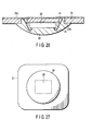
- FIG. 26 is a sectional view of the IC module and FIG. 27 is a diagram of the IC module viewed from the arrow in FIG. 26.
- reference numeral 21 indicates a substrate.
- the substrate 21 has an external terminal 21a on one side and an LSI 23 on the other side.
- the external terminal 21a has a terminal 24.
- the terminal 24 is opposed to a hole 21b formed in the substrate 21.
- the terminal 24 and LSI 23 are electrically connected to each other through gold wire 25 as a connection member.
- the LSI 23 and gold wire 25 are covered with a resin-made protection member 26 to be protected from external pressure.
- the IC module so configured is held and fitted into a holding recess formed in a card base.
- the protection member 26 is hemispherically formed and its central part is increased in thickness; therefore, it does not present strength problems but the following problem.
- the central part of the protection member 26 is thick, if the card base of the IC card is also thick, no problems occur. In this case, however, the card base is often thin. If, therefore, the protection member 26 is thick, the IC module cannot be held in the holding recess.
- the holding recess of the card base is formed deeply to excess, the IC module can be held therein. However, the inner bottom of the holding recess is thinned and cracked if a load is repeatedly applied to the card base.
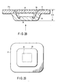
- the protection member 26 of the LSI 23 can be formed to have a trapezoidal section and thus decrease in thickness, as shown in FIGS. 28 and 29.
- the following problems occur.
- the IC module in itself decreases in strength. If an external pressure such as bending and torsion is repeatedly applied to the IC card, the LSI 23 is destroyed or the gold wire 25 becomes poor in connection to thereby cause a malfunction.
- the inner bottom of the holding recess of the card base is flattened. If an external pressure such as bending and torsion is applied to the IC card, stress is concentrated on the inner bottom of the holding recess. This concentration of stress causes problems that the card base is destroyed and the IC module is broken.
- the present invention has been developed in consideration of the above situation and an object thereof is to provide a portable electronic device in which an IC module or a card base is not destroyed even though an external pressure such as bending and torsion is applied to an IC card.
- a portable electronic device comprises a card base having a holding recess; an IC module having a substrate, an LSI mounted on the substrate, and a protection member which covers the LSI, the IC module being held in the holding recess from the protection member; and a reinforcing projection that is formed along a circumference of a surface of the protection member which faces an inner bottom of the holding recess.
- a portable electronic device comprises a card base having a holding recess; an IC module having a substrate, an LSI one surface of which is mounted on one surface of the substrate, a contact terminal provided on other surface of the substrate, a connection member one end of which is electrically connected to the contact terminal and other end of which is electrically connected to other surface of the LSI to form a loop, and a protection member which covers the LSI and the connection member, the IC module being held in the holding recess of the card base from the protection member; and a reinforcing projection that is formed along a circumference of a surface of the protection member which faces an inner bottom of the holding recess to cover the loop of the connection member.
- a portable electronic device comprises a card base having a first holding recess, a second holding recess formed in an inner bottom of the first holding recess, and an irregularity portion formed in an inner bottom of the second holding recess; and an IC module having a substrate, an LSI mounted on the substrate, and a protection member which covers the LSI, the substrate being held in the first holding recess and the protection member being inserted in the second holding recess.
- a portable electronic device comprises a card base having a first holding recess, a second holding recess formed in an inner bottom of the first holding recess, and an irregularity portion formed in an inner bottom of the second holding recess; an IC module having a substrate, an LSI mounted on the substrate, and a protection member which covers the LSI, the substrate being held in the first holding recess and the protection member being inserted in the second holding recess; and a reinforcing projection that is formed along a circumference of a surface of the protection member which faces the inner bottom of the second holding recess, the irregularity portion having a projection which is inserted inside the reinforcing projection.
- FIG. 1 is a plan view showing an IC card according to an embodiment of the present invention as a portable electronic device.
- the IC card includes a card base K and an IC module 1 mounted on the card base K.
- FIG. 2 is a plan view of the card base K from which the IC module 1 is detached.
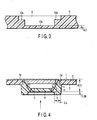
- FIG. 3 is a sectional view taken along line B-B in FIG. 2.
- the card base K has a holding recess 9 that holds the IC module 1.
- the holding recess 9 includes a first holding recess 10a that holds a collar section 7 (described later) of the IC module 1 and a second holding recess 10b that holds a resin-made protection member 6 that covers an LSI 3 (described later).
- FIG. 4 is a sectional view showing an IC module 1 according to a first embodiment of the present invention.
- FIG. 5 is a diagram of the IC module 1 viewed from the arrow in FIG. 4.
- the IC module 1 includes a substrate 2.
- the substrate 2 has a contact terminal 1a on one side and the LSI 3 on the other side.
- the LSI 3 becomes communicable when the contact terminal' 1a contacts an external terminal.
- the contact terminal 1a has a terminal 4.
- the terminal 4 is opposed to a hole 2a formed in the substrate 2.
- the terminal 4 and LSI 3 are electrically connected to each other through gold wire 5 of a connection member.
- the periphery of the LSI 3 is covered with a resin-made protection member 6.
- the protection member 6 protects the LSI 3 and gold wire 5 from external pressure.
- the periphery of the protection member 6 in the substrate 2 serves as a collar section 7.
- a rectangular frame-like reinforcing rib 11 is formed as a reinforcing projection along the circumference of the undersurface of the protection member in FIG. 4.
- the reinforcing rib 11 is integrated with the protection member 6 as one component.
- the IC module 1 so configured is inserted into the holding recess 9 of the card base K from the protection member 6 and held therein.
- the protection member 6 that covers the LSI 3 is held in the second holding recess 10b that is formed deeply, while the collar section 7 is held in the first holding recess 10a that is formed shallowly.
- the reinforcing rib 11 is formed on the undersurface of the protection member 6 integrally with each other as one component. It can therefore receive bending stress of the IC card to increase the strength of the IC card against bending. Consequently, the IC card can be improved in reliability by lessening the drawbacks of poor connection of the gold wire 5 and damage to the LSI 3.
- Table 1 shows results of bending strength tests on the prior art IC module 21 shown in FIG. 28 and the IC module 1 of the present embodiment shown in FIG. 4.
- the thickness of the prior art IC module 21 is 0.51 mm, while the thickness of the IC module 1 is 0.51 mm, the height of the reinforcing rib 11 of the IC module 1 is 0.08 mm, and the width thereof is 1.5 mm.
- the breaking load of the prior art IC module 21 in the first test was 11.93N
- that in the second test was 11.56N and that in the third test was 11.54N
- the average of these breaking loads was 11.54N
- the breaking load of the IC module 1 in the first test was 13.14N
- that in the second test was 13.28N
- that in the third test was 13.28N
- the average of these breaking loads was 13.23N.
- the IC module 1 shown in FIG. 4 is more improved in strength than the prior art IC module 21 shown in FIG. 28.
- FIG. 7 is a sectional view showing an IC module 1 according to a second embodiment of the present invention.
- FIG. 8 is a diagram of the IC module 1 viewed from the arrow in FIG. 7.
- the same components as those of the IC module according to the first embodiment are denoted by the same reference numerals and their descriptions are omitted.
- a protection member 6 for protecting an LSI 3 is hemispherically shaped.
- a circular reinforcing rib 11 is formed on the surface of the protection member 6 as a circular reinforcing projection.
- the reinforcing rib 11 is integrated with the protection member 6 as one component.
- FIG. 9 is a sectional view showing an IC module 1 according to a third embodiment of the present invention.
- FIG. 10 is a diagram of the IC module 1 viewed from the arrow in FIG. 9. The same components as those of the IC module according to the first embodiment are denoted by the same reference numerals and their descriptions are omitted.
- the IC module 1 of the third embodiment has a rectangular frame-like reinforcing rib 11 on the undersurface of a protection member 6 that protects an LSI 3, like that of the first embodiment.
- the IC module 1 also has a reinforcing rib 13a on the undersurface of the protection member 6 as a lattice-like reinforcing projection.
- the reinforcing rib 13a is located inside the reinforcing rib 11 and integrated with the protection member 6 as one component.
- the lattice-like reinforcing rib 13a can increase the strength of the module 1 against the bending of a card further and decrease the drawbacks of poor connection of gold wire 5 and damage to the LSI 3 to improve the reliability of the card further.
- the IC module of the first embodiment is disadvantageous when a load is concentrated on a relatively thin portion of the protection member 6 inside the rectangular frame-like reinforcing rib 11.
- the lattice-like reinforcing rib 13a is formed on a thin portion of the protection member 6. The IC card is therefore strengthened against concentrated load as well as bending and improved in reliability.
- FIG. 11 is a sectional view showing an IC module 1 according to a fourth embodiment of the present invention.
- FIG. 12 is a diagram of the IC module 1 viewed from the arrow in FIG. 11. The same components as those of the IC module according to the first embodiment are denoted by the same reference numerals and their descriptions are omitted.
- gold wire 5 that connects an LSI 3 and a terminal 4 is formed like a loop under the LSI 3.
- the undersurface of the LSI 3 is flat.
- a loop portion 5a of the gold wire 5 projects downward from the undersurface of the LSI 3.
- a rectangular frame-like reinforcing rib 11 is formed to cover the most projected loop portion 5a of the gold wire 5.
- the protection member 6 inside the reinforcing rib 11 need not be thickened more than the amount of projection of the loop portion 5a and accordingly the IC module 1 can be thinned. Consequently, the inner bottom of a holding recess 9 of a card base K can be thickened to decrease damage to the card base K even though a load is applied to the card base K.
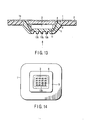
- FIG. 13 is a sectional view showing an IC module 1 according to a fifth embodiment of the present invention.
- FIG. 14 is a diagram of the IC module 1 viewed from the arrow in FIG. 13.
- the same components as those of the IC module according to the fourth embodiment are denoted by the same reference numerals and their descriptions are omitted.
- a lattice-like reinforcing rib 13b is formed as a projection on the undersurface of a protection member 6 inside a frame-like reinforcing rib 11 as shown in the fourth embodiment.
- the reinforcing rib 13b is integrated with the protection member 6 as one component.
- the fifth embodiment can produce the same advantages as those of the fourth embodiment.
- the lattice-like reinforcing rig 13b strengthens the IC card against concentrated load as well as bending to thereby improve the reliability of the IC card.
- the shape of the above-described reinforcing ribs 11, 13a and 13b is not limited to a rectangular frame, a circular frame or a lattice.
- the ribs can be shaped like a single line or a cross.
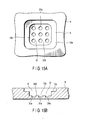
- FIG. 15A is a plan view of a first modification to the holding recess 9 of the card base K and FIG. 15B is a sectional view of the first modification.
- the holding recess 9 of the first modification has an irregularity portion 31 in the inner bottom of the second holding recess 10b.
- the irregularity portion 31 includes a plurality of circular recesses 31a that are vertically and horizontally formed in the inner bottom of the second holding recess 10b and projections 31b that are formed in accordance with the recesses 31a.
- the irregularity portion 31 even though stress is generated at the inner bottom of the second holding recess 10b by applying a great external pressure such as bending and torsion to the card base K, it can be dispersed by the irregularity portion 31 to prevent the card base K from being broken and prevent the IC module 1 from being destroyed.
- FIG. 16 is a plan view of a second modification to the holding recess 9 of the card base K and FIG. 17 is a sectional view of the second modification.
- the holding recess 9 of the second modification has an irregularity portion 33 in the inner bottom of the second holding recess 10b.
- the irregularity portion 33 includes recesses 33a that are formed like a lattice and a plurality of projections 33b that are formed in accordance with the recesses 33a.
- the second modification can also produce the same advantages as those of the first modification.
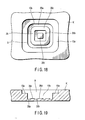
- FIG. 18 is a plan view of a third modification to the holding recess 9 of the card base K and FIG. 19 is a sectional view of the second modification.
- the holding recess 9 of the third modification has an irregularity portion 35 in the inner bottom of the second holding recess 10b.
- the irregularity portion 35 includes first and second ring-shaped recesses 35a and 35b that are formed in the inner bottom of the second holding recess 10b and first and second projections 35c and 35d that are formed in accordance with the first and second recesses 35a and 35b.
- the third modification can also produce the same advantages as those of the first modification.
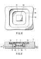
- FIG. 20 is a plan view of a fourth modification to the holding recess 9 of the card base K.
- the holding recess 9 of the fourth modification has an irregularity portion 38 in the inner bottom of the second holding recess 10b.
- the irregularity portion 38 includes a rectangular projection 38a that projects from the central part of the inner bottom of the second holding recess 10b and a recess 38b that is formed in accordance with the projection 38a.
- the IC module 1 as shown in FIG. 4 is held in the holding recess 9 as shown in FIG. 21.
- the projection 38a is inserted inside the reinforcing rib 11 of the protection member 6 of the LSI 3.
- the card can be thinned only by inserting the projection 38a inside the reinforcing rib 11.
- Table 2 shows results of bending strength tests on the prior art IC module 21 shown in FIG. 28, which is held in the holding recess 9 of the card base K shown in FIG. 3 and formed as a card, and the IC module 1 which is formed as a card as shown in FIG. 21.
- the thickness of the bottom of the second holding recess 10b of the card base K shown in FIG. 3 is 0.2 mm, while the thickness of the projection 38a of the second holding recess 10b of the card base K shown in FIG. 21 is 0.2 mm and the depth of the recess 38b is 0.08 mm.
- the breaking load of the prior art card in the first test was 20.09N
- that in the second test was 20.58N and that in the third test was 20.97N
- the average of these breaking loads was 20.55N
- the breaking load. of the card shown in FIG. 21 in the first test was 24.65N
- that in the second test was 24.55N and that in the third test was 25.07N
- the average of these breaking loads was 24.76N.
- the card shown in FIG. 21 is more improved in strength than the prior art card.
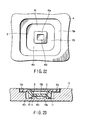
- FIG. 22 is a plan view of a fifth modification to the holding recess 9 of the card base K.
- the holding recess 9 of the fifth modification has an irregularity portion 40 in the inner bottom of the second holding recess 10b.
- the irregularity portion 40 includes a rectangular frame-like projection 40a and recesses 40b and 40c that are formed in accordance with the projection 40a.
- the projection 40a is inserted inside the reinforcing rib 11 of the protection member 6 of the LSI 3 as shown in FIG. 23.
- the fifth modification can also produce the same advantages as those of the fourth modification.
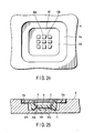
- FIG. 24 is a plan view of a sixth modification to the holding recess 9 of the card base K.
- the holding recess 9 of the sixth modification has an irregularity portion 42 in the inner bottom of the second holding recess 10b.
- the irregularity portion 42 includes a plurality of projections 42a that are formed vertically and horizontally in the central part of the inner bottom of the second holding recess 10b and recesses 42b that are formed in accordance with the projections 42a.
- the projections 42a are inserted inside the reinforcing rib 11 of the protection member 6.
- the sixth modification can also produce the same advantages as those of the fourth modification.
Landscapes
- Engineering & Computer Science (AREA)
- Computer Hardware Design (AREA)
- Microelectronics & Electronic Packaging (AREA)
- Physics & Mathematics (AREA)
- General Physics & Mathematics (AREA)
- Theoretical Computer Science (AREA)
- Credit Cards Or The Like (AREA)
- Structures Or Materials For Encapsulating Or Coating Semiconductor Devices Or Solid State Devices (AREA)
Abstract
Description
- The present invention relates to a portable electronic device such as an IC card that is improved in IC module and IC module holding recess.
- An IC module for IC cards as shown in FIGS. 26 and 27 is known. FIG. 26 is a sectional view of the IC module and FIG. 27 is a diagram of the IC module viewed from the arrow in FIG. 26.
- In FIGS. 26 and 27,
reference numeral 21 indicates a substrate. Thesubstrate 21 has anexternal terminal 21a on one side and anLSI 23 on the other side. Theexternal terminal 21a has aterminal 24. Theterminal 24 is opposed to ahole 21b formed in thesubstrate 21. Theterminal 24 and LSI 23 are electrically connected to each other throughgold wire 25 as a connection member. TheLSI 23 andgold wire 25 are covered with a resin-madeprotection member 26 to be protected from external pressure. The IC module so configured is held and fitted into a holding recess formed in a card base. - However, conventionally, the
protection member 26 is hemispherically formed and its central part is increased in thickness; therefore, it does not present strength problems but the following problem. - When the central part of the
protection member 26 is thick, if the card base of the IC card is also thick, no problems occur. In this case, however, the card base is often thin. If, therefore, theprotection member 26 is thick, the IC module cannot be held in the holding recess. - If the holding recess of the card base is formed deeply to excess, the IC module can be held therein. However, the inner bottom of the holding recess is thinned and cracked if a load is repeatedly applied to the card base.
- To resolve the above problem, the
protection member 26 of theLSI 23 can be formed to have a trapezoidal section and thus decrease in thickness, as shown in FIGS. 28 and 29. In this case, however, the following problems occur. The IC module in itself decreases in strength. If an external pressure such as bending and torsion is repeatedly applied to the IC card, theLSI 23 is destroyed or thegold wire 25 becomes poor in connection to thereby cause a malfunction. - Conventionally, the inner bottom of the holding recess of the card base is flattened. If an external pressure such as bending and torsion is applied to the IC card, stress is concentrated on the inner bottom of the holding recess. This concentration of stress causes problems that the card base is destroyed and the IC module is broken.
- The present invention has been developed in consideration of the above situation and an object thereof is to provide a portable electronic device in which an IC module or a card base is not destroyed even though an external pressure such as bending and torsion is applied to an IC card.
- A portable electronic device according to a first aspect of the present invention, comprises a card base having a holding recess; an IC module having a substrate, an LSI mounted on the substrate, and a protection member which covers the LSI, the IC module being held in the holding recess from the protection member; and a reinforcing projection that is formed along a circumference of a surface of the protection member which faces an inner bottom of the holding recess.
- A portable electronic device according to a second aspect of the present invention, comprises a card base having a holding recess; an IC module having a substrate, an LSI one surface of which is mounted on one surface of the substrate, a contact terminal provided on other surface of the substrate, a connection member one end of which is electrically connected to the contact terminal and other end of which is electrically connected to other surface of the LSI to form a loop, and a protection member which covers the LSI and the connection member, the IC module being held in the holding recess of the card base from the protection member; and a reinforcing projection that is formed along a circumference of a surface of the protection member which faces an inner bottom of the holding recess to cover the loop of the connection member.
- A portable electronic device according to a third aspect of the present invention, comprises a card base having a first holding recess, a second holding recess formed in an inner bottom of the first holding recess, and an irregularity portion formed in an inner bottom of the second holding recess; and an IC module having a substrate, an LSI mounted on the substrate, and a protection member which covers the LSI, the substrate being held in the first holding recess and the protection member being inserted in the second holding recess.
- A portable electronic device according to a fourth aspect of the present invention, comprises a card base having a first holding recess, a second holding recess formed in an inner bottom of the first holding recess, and an irregularity portion formed in an inner bottom of the second holding recess; an IC module having a substrate, an LSI mounted on the substrate, and a protection member which covers the LSI, the substrate being held in the first holding recess and the protection member being inserted in the second holding recess; and a reinforcing projection that is formed along a circumference of a surface of the protection member which faces the inner bottom of the second holding recess, the irregularity portion having a projection which is inserted inside the reinforcing projection.
- This summary of the invention does not necessarily describe all necessary features so that the invention may also be a sub-combination of these described features.
- The invention can be more fully understood from the following detailed description when taken in conjunction with the accompanying drawings, in which:
- FIG. 1 is a plan view showing an IC card according to an embodiment of the present invention.
- FIG. 2 is a plan view showing a card base of the IC card.
- FIG. 3 is a sectional view taken along line B-B in FIG. 2.
- FIG. 4 is a sectional view of an IC module according to a first embodiment of the present invention, which is mounted on the IC card.
- FIG. 5 is a diagram of the IC module viewed from the arrow in FIG. 4.
- FIG. 6 is a sectional view taken along line A-A in FIG. 1.
- FIG. 7 is a sectional view of an IC module according to a second embodiment of the present invention, which is mounted on the IC card.
- FIG. 8 is a diagram of the IC module viewed from the arrow in FIG. 7.
- FIG. 9 is a sectional view of an IC module according to a third embodiment of the present invention, which is mounted on the IC card.
- FIG. 10 is a diagram of the IC module viewed from the arrow in FIG. 9.
- FIG. 11 is a sectional view of an IC module according to a fourth embodiment of the present invention, which is mounted on the IC card.
- FIG. 12 is a diagram of the IC module viewed from the arrow in FIG. 11.
- FIG. 13 is a sectional view of an IC module according to a fifth embodiment of the present invention, which is mounted on the IC card.
- FIG. 14 is a diagram of the IC module viewed from the arrow in FIG. 13.
- FIG. 15A is a plan view showing a first modification to the holding recess of the card base of the IC card.
- FIG. 15B is a sectional side view of the holding recess shown in FIG. 15A.
- FIG. 16 is a plan view showing a second modification to the holding recess of the card base.
- FIG. 17 is a sectional side view of the second modification to the holding recess.
- FIG. 18 is a plan view showing a third modification to the holding recess of the card base.
- FIG. 19 is a sectional side view of the third modification to the holding recess.
- FIG. 20 is a plan view showing a fourth modification to the holding recess of the card base.
- FIG. 21 is a sectional side view of the fourth modification to the holding recess in which the IC module shown in FIG. 4 is held.
- FIG. 22 is a plan view showing a fifth modification to the holding recess of the card base.
- FIG. 23 is a sectional side view of the fifth modification to the holding recess in which the IC module shown in FIG. 4 is held.
- FIG. 24 is a plan view showing a sixth modification to the holding recess of the card base.
- FIG. 25 is a sectional side view of the sixth modification to the holding recess in which the IC module shown in FIG. 4 is held.
- FIG. 26 is a sectional view showing a first prior art IC module.
- FIG. 27 is a diagram of the first prior art IC module viewed from the arrow in FIG. 26.
- FIG. 28 is a sectional view showing a second prior art IC module.
- FIG. 29 is a diagram of the second prior art IC module viewed from the arrow in FIG. 28.
-
- Embodiments of the present invention will be described below with reference to the accompanying drawings.
- FIG. 1 is a plan view showing an IC card according to an embodiment of the present invention as a portable electronic device. The IC card includes a card base K and an
IC module 1 mounted on the card base K. - FIG. 2 is a plan view of the card base K from which the
IC module 1 is detached. FIG. 3 is a sectional view taken along line B-B in FIG. 2. - The card base K has a holding
recess 9 that holds theIC module 1. The holdingrecess 9 includes afirst holding recess 10a that holds a collar section 7 (described later) of theIC module 1 and asecond holding recess 10b that holds a resin-madeprotection member 6 that covers an LSI 3 (described later). - FIG. 4 is a sectional view showing an
IC module 1 according to a first embodiment of the present invention. FIG. 5 is a diagram of theIC module 1 viewed from the arrow in FIG. 4. - The
IC module 1 includes asubstrate 2.
Thesubstrate 2 has acontact terminal 1a on one side and theLSI 3 on the other side. TheLSI 3 becomes communicable when the contact terminal' 1a contacts an external terminal. Thecontact terminal 1a has aterminal 4. Theterminal 4 is opposed to ahole 2a formed in thesubstrate 2. Theterminal 4 andLSI 3 are electrically connected to each other throughgold wire 5 of a connection member. The periphery of theLSI 3 is covered with a resin-madeprotection member 6. Theprotection member 6 protects theLSI 3 andgold wire 5 from external pressure. The periphery of theprotection member 6 in thesubstrate 2 serves as acollar section 7. - A rectangular frame-like reinforcing
rib 11 is formed as a reinforcing projection along the circumference of the undersurface of the protection member in FIG. 4. The reinforcingrib 11 is integrated with theprotection member 6 as one component. - The
IC module 1 so configured is inserted into the holdingrecess 9 of the card base K from theprotection member 6 and held therein. In other words, theprotection member 6 that covers theLSI 3 is held in thesecond holding recess 10b that is formed deeply, while thecollar section 7 is held in thefirst holding recess 10a that is formed shallowly. - As described above, the reinforcing
rib 11 is formed on the undersurface of theprotection member 6 integrally with each other as one component. It can therefore receive bending stress of the IC card to increase the strength of the IC card against bending. Consequently, the IC card can be improved in reliability by lessening the drawbacks of poor connection of thegold wire 5 and damage to theLSI 3.
- Table 1 shows results of bending strength tests on the prior
art IC module 21 shown in FIG. 28 and theIC module 1 of the present embodiment shown in FIG. 4. The thickness of the priorart IC module 21 is 0.51 mm, while the thickness of theIC module 1 is 0.51 mm, the height of the reinforcingrib 11 of theIC module 1 is 0.08 mm, and the width thereof is 1.5 mm. - Three tests on each of the
IC modules art IC module 21 in the first test was 11.93N, that in the second test was 11.56N and that in the third test was 11.54N, and the average of these breaking loads was 11.54N. On the other hand, the breaking load of theIC module 1 in the first test was 13.14N, that in the second test was 13.28N and that in the third test was 13.28N, and the average of these breaking loads was 13.23N. - As is evident from the above results, the
IC module 1 shown in FIG. 4 is more improved in strength than the priorart IC module 21 shown in FIG. 28. - FIG. 7 is a sectional view showing an
IC module 1 according to a second embodiment of the present invention. FIG. 8 is a diagram of theIC module 1 viewed from the arrow in FIG. 7. The same components as those of the IC module according to the first embodiment are denoted by the same reference numerals and their descriptions are omitted. - In the second embodiment, a
protection member 6 for protecting anLSI 3 is hemispherically shaped. A circular reinforcingrib 11 is formed on the surface of theprotection member 6 as a circular reinforcing projection. The reinforcingrib 11 is integrated with theprotection member 6 as one component. The second embodiment can produce the same advantages as those of the first embodiment. - FIG. 9 is a sectional view showing an
IC module 1 according to a third embodiment of the present invention. FIG. 10 is a diagram of theIC module 1 viewed from the arrow in FIG. 9. The same components as those of the IC module according to the first embodiment are denoted by the same reference numerals and their descriptions are omitted. - The
IC module 1 of the third embodiment has a rectangular frame-like reinforcingrib 11 on the undersurface of aprotection member 6 that protects anLSI 3, like that of the first embodiment. TheIC module 1 also has a reinforcingrib 13a on the undersurface of theprotection member 6 as a lattice-like reinforcing projection. The reinforcingrib 13a is located inside the reinforcingrib 11 and integrated with theprotection member 6 as one component. The lattice-like reinforcingrib 13a can increase the strength of themodule 1 against the bending of a card further and decrease the drawbacks of poor connection ofgold wire 5 and damage to theLSI 3 to improve the reliability of the card further. - The IC module of the first embodiment is disadvantageous when a load is concentrated on a relatively thin portion of the
protection member 6 inside the rectangular frame-like reinforcingrib 11. In the third embodiment, however, the lattice-like reinforcingrib 13a is formed on a thin portion of theprotection member 6. The IC card is therefore strengthened against concentrated load as well as bending and improved in reliability. - FIG. 11 is a sectional view showing an
IC module 1 according to a fourth embodiment of the present invention. FIG. 12 is a diagram of theIC module 1 viewed from the arrow in FIG. 11. The same components as those of the IC module according to the first embodiment are denoted by the same reference numerals and their descriptions are omitted. - In the fourth embodiment,
gold wire 5 that connects anLSI 3 and aterminal 4 is formed like a loop under theLSI 3. Usually, the undersurface of theLSI 3 is flat. In order to connect thegold wire 5 to the flat undersurface of theLSI 3, aloop portion 5a of thegold wire 5 projects downward from the undersurface of theLSI 3. - In the fourth embodiment, a rectangular frame-like reinforcing
rib 11 is formed to cover the most projectedloop portion 5a of thegold wire 5. Theprotection member 6 inside the reinforcingrib 11 need not be thickened more than the amount of projection of theloop portion 5a and accordingly theIC module 1 can be thinned. Consequently, the inner bottom of a holdingrecess 9 of a card base K can be thickened to decrease damage to the card base K even though a load is applied to the card base K. - FIG. 13 is a sectional view showing an
IC module 1 according to a fifth embodiment of the present invention. FIG. 14 is a diagram of theIC module 1 viewed from the arrow in FIG. 13. The same components as those of the IC module according to the fourth embodiment are denoted by the same reference numerals and their descriptions are omitted. - In the fifth embodiment, a lattice-like reinforcing
rib 13b is formed as a projection on the undersurface of aprotection member 6 inside a frame-like reinforcingrib 11 as shown in the fourth embodiment. The reinforcingrib 13b is integrated with theprotection member 6 as one component. - The fifth embodiment can produce the same advantages as those of the fourth embodiment. The lattice-like reinforcing
rig 13b strengthens the IC card against concentrated load as well as bending to thereby improve the reliability of the IC card. - The shape of the above-described reinforcing
ribs - FIG. 15A is a plan view of a first modification to the holding
recess 9 of the card base K and FIG. 15B is a sectional view of the first modification. - The holding
recess 9 of the first modification has anirregularity portion 31 in the inner bottom of thesecond holding recess 10b. Theirregularity portion 31 includes a plurality ofcircular recesses 31a that are vertically and horizontally formed in the inner bottom of thesecond holding recess 10b andprojections 31b that are formed in accordance with therecesses 31a. - According to the first modification, even though stress is generated at the inner bottom of the
second holding recess 10b by applying a great external pressure such as bending and torsion to the card base K, it can be dispersed by theirregularity portion 31 to prevent the card base K from being broken and prevent theIC module 1 from being destroyed. - FIG. 16 is a plan view of a second modification to the holding
recess 9 of the card base K and FIG. 17 is a sectional view of the second modification. - The holding
recess 9 of the second modification has anirregularity portion 33 in the inner bottom of thesecond holding recess 10b. Theirregularity portion 33 includesrecesses 33a that are formed like a lattice and a plurality ofprojections 33b that are formed in accordance with therecesses 33a. - The second modification can also produce the same advantages as those of the first modification.
- FIG. 18 is a plan view of a third modification to the holding
recess 9 of the card base K and FIG. 19 is a sectional view of the second modification. - The holding
recess 9 of the third modification has anirregularity portion 35 in the inner bottom of thesecond holding recess 10b. Theirregularity portion 35 includes first and second ring-shapedrecesses second holding recess 10b and first andsecond projections second recesses - The third modification can also produce the same advantages as those of the first modification.
- FIG. 20 is a plan view of a fourth modification to the holding
recess 9 of the card base K. - The holding
recess 9 of the fourth modification has anirregularity portion 38 in the inner bottom of thesecond holding recess 10b. Theirregularity portion 38 includes arectangular projection 38a that projects from the central part of the inner bottom of thesecond holding recess 10b and arecess 38b that is formed in accordance with theprojection 38a. TheIC module 1 as shown in FIG. 4 is held in the holdingrecess 9 as shown in FIG. 21. In other words, theprojection 38a is inserted inside the reinforcingrib 11 of theprotection member 6 of theLSI 3. - According to the fourth modification, not only the same advantages as those of the first modification can be obtained, but also the card can be thinned only by inserting the
projection 38a inside the reinforcingrib 11.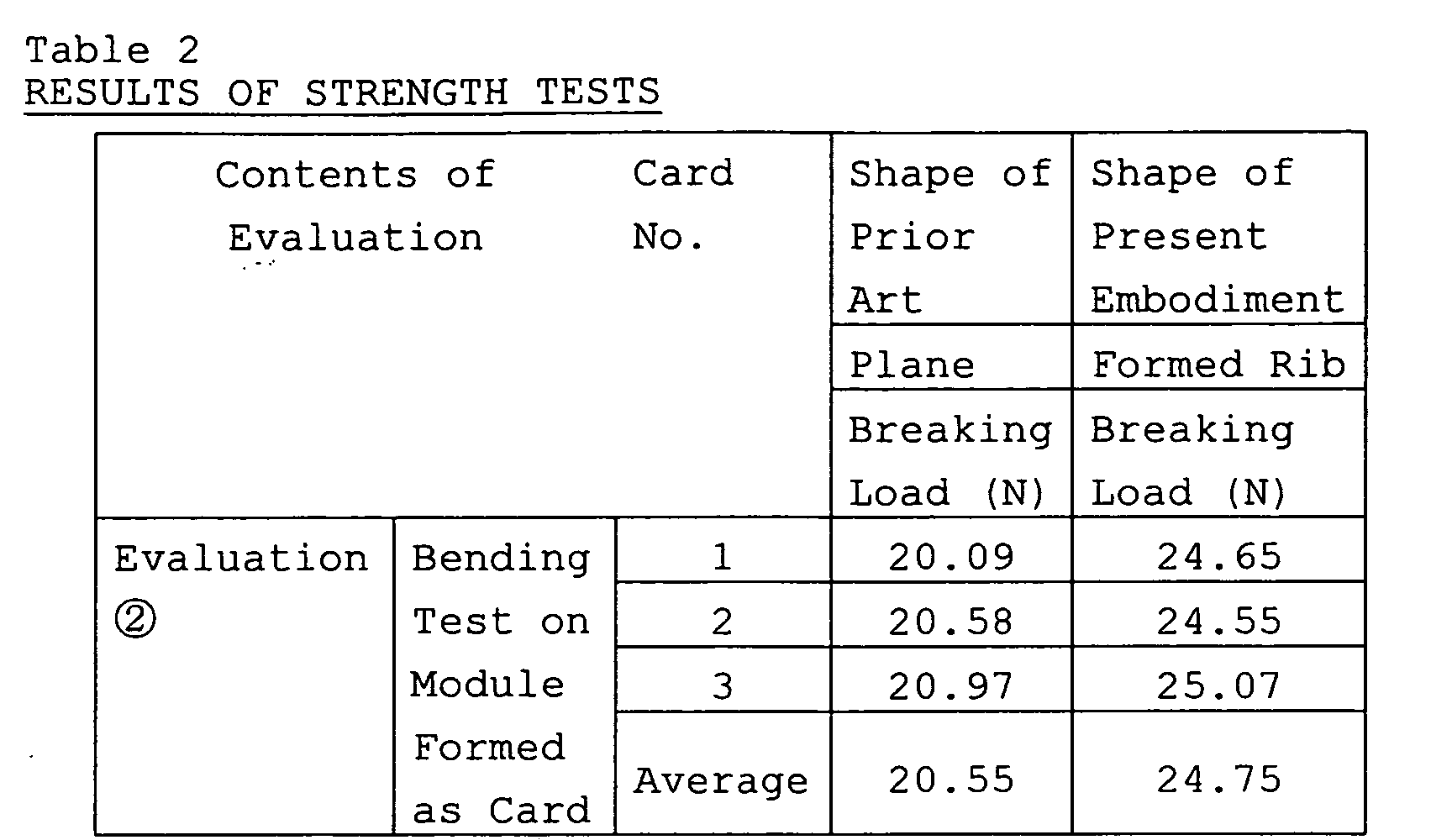
- Table 2 shows results of bending strength tests on the prior
art IC module 21 shown in FIG. 28, which is held in the holdingrecess 9 of the card base K shown in FIG. 3 and formed as a card, and theIC module 1 which is formed as a card as shown in FIG. 21. The thickness of the bottom of thesecond holding recess 10b of the card base K shown in FIG. 3 is 0.2 mm, while the thickness of theprojection 38a of thesecond holding recess 10b of the card base K shown in FIG. 21 is 0.2 mm and the depth of therecess 38b is 0.08 mm. - Three tests on each of the above prior art card and the card shown in FIG. 21 were conducted and an average of the tests was taken. The breaking load of the prior art card in the first test was 20.09N, that in the second test was 20.58N and that in the third test was 20.97N, and the average of these breaking loads was 20.55N. On the other hand, the breaking load. of the card shown in FIG. 21 in the first test was 24.65N, that in the second test was 24.55N and that in the third test was 25.07N, and the average of these breaking loads was 24.76N.
- As is evident from the above results, the card shown in FIG. 21 is more improved in strength than the prior art card.
- FIG. 22 is a plan view of a fifth modification to the holding
recess 9 of the card base K. - The holding
recess 9 of the fifth modification has anirregularity portion 40 in the inner bottom of thesecond holding recess 10b. Theirregularity portion 40 includes a rectangular frame-like projection 40a and recesses 40b and 40c that are formed in accordance with theprojection 40a. Theprojection 40a is inserted inside the reinforcingrib 11 of theprotection member 6 of theLSI 3 as shown in FIG. 23. - The fifth modification can also produce the same advantages as those of the fourth modification.
- FIG. 24 is a plan view of a sixth modification to the holding
recess 9 of the card base K. - The holding
recess 9 of the sixth modification has anirregularity portion 42 in the inner bottom of thesecond holding recess 10b. Theirregularity portion 42 includes a plurality ofprojections 42a that are formed vertically and horizontally in the central part of the inner bottom of thesecond holding recess 10b and recesses 42b that are formed in accordance with theprojections 42a. Theprojections 42a are inserted inside the reinforcingrib 11 of theprotection member 6. - The sixth modification can also produce the same advantages as those of the fourth modification.
- It is explicitly stated that all features disclosed in the description and/or the claims are intended to be disclosed separately and independently from each other for the purpose of original disclosure as well as for the purpose of restricting the claimed invention independent of the composition of the features in the embodiments and/or the claims. It is explicitly stated that all value ranges or indications of groups of entities disclose every possible intermediate value or intermediate entity for the purpose of original disclosure as well as for the purpose of restricting the claimed invention, in particular as limits of value ranges.
Claims (15)
- A portable electronic device comprising:characterized by further comprising a reinforcing projection (11) that is formed along a circumference of a surface of the protection member (6) which faces an inner bottom of the holding recess (9).a card base (K) having a holding recess (9); andan IC module (1) having a substrate (2), an LSI (3) mounted on the substrate (2), and a protection member (6) which covers the LSI (3), the IC module (1) being held in the holding recess (9) from the protection member (6),
- The portable electronic device according to claim 1, characterized in that the projection (11) is shaped like a rectangular frame.
- The portable electronic device according to claim 1, characterized in that the projection (11) is shaped like a circular frame.
- The portable electronic device according to claim 2, characterized in that a lattice-like projection (13a) is formed inside the projection (11) shaped like the rectangular frame.
- A portable electronic device comprising:characterized by further comprising a reinforcing projection (11) that is formed along a circumference of a surface of the protection member (6) which faces an inner bottom of the holding recess (9) to cover the loop of the connection member (5).a card base (K) having a holding recess (9); andan IC module (1) having a substrate (2), an LSI (3) one surface of which is mounted on one surface of the substrate (2), a contact terminal (1a) provided on other surface of the substrate (2), a connection member (5) one end of which is electrically connected to the contact terminal (1a) and other end of which is electrically connected to other surface of the LSI (3) to form a loop, and a protection member (6) which covers the LSI (3) and the connection member (5), the IC module (1) being held in the holding recess (9) of the card base (K) from the protection member (6),
- The portable electronic device according to claim 5, characterized in that the projection (11) is shaped like a rectangular frame.
- The portable electronic device according to claim 6, characterized in that a lattice-like projection (13b) is formed inside the projection (11) shaped like the rectangular frame.
- A portable electronic device comprising:characterized in that an irregularity portion (31, 33, 35) is formed in an inner bottom of the second holding recess (10b) of the card base (K).a card base (K) having a first holding recess (10a) and a second holding recess (10b) formed in an inner bottom of the first holding recess (10a); andan IC module (1) having a substrate (2), an LSI (3) mounted on the substrate (2), and a protection member (6) which covers the LSI (3), the substrate (2) being held in the first holding recess (10a) and the protection member (6) being inserted in the second holding recess (10b),
- The portable electronic device according to claim 8, characterized in that the irregularity portion (31) has a plurality of circular recesses (31a).
- The portable electronic device according to claim 8, characterized in that the irregularity portion (33) has a lattice-like recess (33a).
- The portable electronic device according to claim 8, characterized in that the irregularity portion (35) has a ring-shaped circular recess (35a, 35b).
- A portable electronic device comprising:characterized in that an irregularity portion (38, 40, 42) is formed in an inner bottom of the second holding recess (10b) of the card base (K);a card base (K) having a first holding recess (10a) and a second holding recess (10b) formed in an inner bottom of the first holding recess (10a); andan IC module (1) having a substrate (2), an LSI (3) mounted on the substrate (2), and a protection member (6) which covers the LSI (3), the substrate (2) being held in the first holding recess (10a) and the protection member (6) being inserted in the second holding recess (10b),
a reinforcing projection (11) is formed along a circumference of a surface of the protection member (6) which faces the inner bottom of the second holding recess (10b); and
the irregularity portion (38, 40, 42) has a projection (38a, 40a, 42a) which is inserted inside the reinforcing projection (11). - The portable electronic device according to claim 12, characterized in that the projection (38a) of the irregularity portion (38) is shaped like a rectangle.
- The portable electronic device according to claim 12, characterized in that the projection (40a) of the irregularity portion (40) is shaped like a rectangular frame.
- The portable electronic device according to claim 12, characterized in that the irregularity portion (42) has a plurality of projections (42a).
Applications Claiming Priority (4)
| Application Number | Priority Date | Filing Date | Title |
|---|---|---|---|
| JP2003336213 | 2003-09-26 | ||
| JP2003336213 | 2003-09-26 | ||
| JP2004092539 | 2004-03-26 | ||
| JP2004092539A JP2005122678A (en) | 2003-09-26 | 2004-03-26 | Portable electronic device |
Publications (2)
| Publication Number | Publication Date |
|---|---|
| EP1519310A2 true EP1519310A2 (en) | 2005-03-30 |
| EP1519310A3 EP1519310A3 (en) | 2005-07-06 |
Family
ID=34197269
Family Applications (1)
| Application Number | Title | Priority Date | Filing Date |
|---|---|---|---|
| EP04022678A Withdrawn EP1519310A3 (en) | 2003-09-26 | 2004-09-23 | Portable electronic device |
Country Status (5)
| Country | Link |
|---|---|
| US (1) | US7063267B2 (en) |
| EP (1) | EP1519310A3 (en) |
| JP (1) | JP2005122678A (en) |
| KR (1) | KR20050030857A (en) |
| CN (1) | CN1601558A (en) |
Cited By (1)
| Publication number | Priority date | Publication date | Assignee | Title |
|---|---|---|---|---|
| CN109638333A (en) * | 2017-10-05 | 2019-04-16 | 卡西欧计算机株式会社 | It is insert-molded method and is insert-molded component |
Families Citing this family (12)
| Publication number | Priority date | Publication date | Assignee | Title |
|---|---|---|---|---|
| US8107875B2 (en) * | 2006-09-26 | 2012-01-31 | Viasat, Inc. | Placement of gateways near service beams |
| DE102007008487A1 (en) * | 2007-02-19 | 2008-08-21 | Smartrac Ip B.V. | Method and semifinished product for producing an inlay |
| DE102011114635A1 (en) * | 2011-10-04 | 2013-04-04 | Smartrac Ip B.V. | Chip card and method for producing a chip card |
| USD707682S1 (en) * | 2012-12-05 | 2014-06-24 | Logomotion, S.R.O. | Memory card |
| US9647997B2 (en) | 2013-03-13 | 2017-05-09 | Nagrastar, Llc | USB interface for performing transport I/O |
| USD758372S1 (en) | 2013-03-13 | 2016-06-07 | Nagrastar Llc | Smart card interface |
| USD729808S1 (en) * | 2013-03-13 | 2015-05-19 | Nagrastar Llc | Smart card interface |
| US9888283B2 (en) | 2013-03-13 | 2018-02-06 | Nagrastar Llc | Systems and methods for performing transport I/O |
| USD759022S1 (en) * | 2013-03-13 | 2016-06-14 | Nagrastar Llc | Smart card interface |
| USD780763S1 (en) * | 2015-03-20 | 2017-03-07 | Nagrastar Llc | Smart card interface |
| USD864968S1 (en) | 2015-04-30 | 2019-10-29 | Echostar Technologies L.L.C. | Smart card interface |
| US12124905B1 (en) * | 2021-12-17 | 2024-10-22 | Wells Fargo Bank, N.A. | Transaction instrument with features for destruction and disposal |
Family Cites Families (18)
| Publication number | Priority date | Publication date | Assignee | Title |
|---|---|---|---|---|
| US4876441A (en) * | 1984-03-27 | 1989-10-24 | Casio Computer Co., Ltd. | Card-like electronic apparatus |
| US4727246A (en) * | 1984-08-31 | 1988-02-23 | Casio Computer Co., Ltd. | IC card |
| US5155068A (en) * | 1989-08-31 | 1992-10-13 | Sharp Kabushiki Kaisha | Method for manufacturing an IC module for an IC card whereby an IC device and surrounding encapsulant are thinned by material removal |
| FR2662000A1 (en) | 1990-05-11 | 1991-11-15 | Philips Composants | MICROCIRCUIT CARD. |
| JPH06199084A (en) | 1992-12-28 | 1994-07-19 | Toshiba Corp | Ic card |
| JP3388921B2 (en) * | 1994-11-29 | 2003-03-24 | 株式会社東芝 | Manufacturing method of integrated circuit card |
| JP3935976B2 (en) * | 1995-02-08 | 2007-06-27 | ヒューレット・パッカード・カンパニー | Semiconductor layer structure and recording medium for large capacity memory device |
| JP3337847B2 (en) * | 1995-02-27 | 2002-10-28 | 株式会社東芝 | Manufacturing method of electronic component built-in card |
| US5854819A (en) * | 1996-02-07 | 1998-12-29 | Canon Kabushiki Kaisha | Mask supporting device and correction method therefor, and exposure apparatus and device producing method utilizing the same |
| US5786988A (en) * | 1996-07-02 | 1998-07-28 | Sandisk Corporation | Integrated circuit chips made bendable by forming indentations in their back surfaces flexible packages thereof and methods of manufacture |
| CN1110770C (en) * | 1997-06-23 | 2003-06-04 | 罗姆股份有限公司 | Moule for IC card, IC card and method for mfg. of module for IC card |
| WO1999004367A1 (en) * | 1997-07-18 | 1999-01-28 | Dai Nippon Printing Co., Ltd. | Ic module, ic card, sealing resin for ic module, and method for manufacturing ic module |
| JPH1185937A (en) * | 1997-09-02 | 1999-03-30 | Nippon Lsi Card Kk | Non-contact lsi card and method for inspecting the same |
| JP3914620B2 (en) * | 1997-10-16 | 2007-05-16 | シチズン時計株式会社 | IC card |
| EP1041624A1 (en) * | 1999-04-02 | 2000-10-04 | Interuniversitair Microelektronica Centrum Vzw | Method of transferring ultra-thin substrates and application of the method to the manufacture of a multilayer thin film device |
| FR2799857A1 (en) * | 1999-10-14 | 2001-04-20 | Gemplus Card Int | METHOD FOR REINFORCING AN INTEGRATED SMART CARD CIRCUIT MODULE |
| JP4802398B2 (en) * | 2001-06-08 | 2011-10-26 | 凸版印刷株式会社 | Non-contact IC card |
| JP3470111B2 (en) * | 2001-06-28 | 2003-11-25 | 松下電器産業株式会社 | Method for manufacturing resin-encapsulated semiconductor device |
-
2004
- 2004-03-26 JP JP2004092539A patent/JP2005122678A/en active Pending
- 2004-09-22 KR KR1020040075713A patent/KR20050030857A/en not_active Abandoned
- 2004-09-23 US US10/947,399 patent/US7063267B2/en not_active Expired - Fee Related
- 2004-09-23 EP EP04022678A patent/EP1519310A3/en not_active Withdrawn
- 2004-09-24 CN CNA2004100117083A patent/CN1601558A/en active Pending
Non-Patent Citations (1)
| Title |
|---|
| None * |
Cited By (3)
| Publication number | Priority date | Publication date | Assignee | Title |
|---|---|---|---|---|
| CN109638333A (en) * | 2017-10-05 | 2019-04-16 | 卡西欧计算机株式会社 | It is insert-molded method and is insert-molded component |
| US11472079B2 (en) | 2017-10-05 | 2022-10-18 | Casio Computer Co., Ltd. | Insert molding method and insert molding component |
| US11731329B2 (en) | 2017-10-05 | 2023-08-22 | Casio Computer Co., Ltd. | Insert molding method and insert molding component |
Also Published As
| Publication number | Publication date |
|---|---|
| US20050082374A1 (en) | 2005-04-21 |
| CN1601558A (en) | 2005-03-30 |
| KR20050030857A (en) | 2005-03-31 |
| EP1519310A3 (en) | 2005-07-06 |
| JP2005122678A (en) | 2005-05-12 |
| US7063267B2 (en) | 2006-06-20 |
Similar Documents
| Publication | Publication Date | Title |
|---|---|---|
| US8678863B2 (en) | Connector and electronic device having the same | |
| US6399418B1 (en) | Method for forming a reduced thickness packaged electronic device | |
| US7063267B2 (en) | Portable electronic device | |
| US8625298B2 (en) | Protection for circuit boards | |
| CN107181076A (en) | Circuit board electrical connector | |
| CN101202275A (en) | Package with shielded case | |
| CN106461474B (en) | force detector | |
| US7884630B2 (en) | IC carrie, IC socket and method for testing IC device | |
| CN202285233U (en) | Semiconductor device | |
| CN102214865A (en) | Elastic contact piece for card connector and card connector equipped with the elastic contact piece | |
| US20200006873A1 (en) | Connector | |
| JP2010198427A (en) | Circuit board module and electronic apparatus including the same | |
| JP2005101283A (en) | Surface mount type light emitting diode | |
| US20100052190A1 (en) | Semiconductor device | |
| TWM288991U (en) | IC socket and IC socket assembly | |
| US8524529B2 (en) | Brace for wire bond | |
| US6353256B1 (en) | IC package structure for achieving better heat dissipation | |
| JP4366472B2 (en) | Semiconductor device | |
| US7838981B2 (en) | Component assembly | |
| KR101773503B1 (en) | Wire to board connector assembly | |
| KR20150089257A (en) | Contact terminal on the board for protecting deformation from side direction | |
| US20070173138A1 (en) | Contact used in an electrical connector | |
| JP4890161B2 (en) | Connecting terminal | |
| JP2001358172A (en) | Semiconductor package | |
| JP3118694B2 (en) | PC card frame |
Legal Events
| Date | Code | Title | Description |
|---|---|---|---|
| PUAI | Public reference made under article 153(3) epc to a published international application that has entered the european phase |
Free format text: ORIGINAL CODE: 0009012 |
|
| 17P | Request for examination filed |
Effective date: 20040923 |
|
| AK | Designated contracting states |
Kind code of ref document: A2 Designated state(s): AT BE BG CH CY CZ DE DK EE ES FI FR GB GR HU IE IT LI LU MC NL PL PT RO SE SI SK TR |
|
| AX | Request for extension of the european patent |
Extension state: AL HR LT LV MK |
|
| PUAL | Search report despatched |
Free format text: ORIGINAL CODE: 0009013 |
|
| AK | Designated contracting states |
Kind code of ref document: A3 Designated state(s): AT BE BG CH CY CZ DE DK EE ES FI FR GB GR HU IE IT LI LU MC NL PL PT RO SE SI SK TR |
|
| AX | Request for extension of the european patent |
Extension state: AL HR LT LV MK |
|
| AKX | Designation fees paid |
Designated state(s): DE FR GB |
|
| 17Q | First examination report despatched |
Effective date: 20061205 |
|
| STAA | Information on the status of an ep patent application or granted ep patent |
Free format text: STATUS: THE APPLICATION IS DEEMED TO BE WITHDRAWN |
|
| 18D | Application deemed to be withdrawn |
Effective date: 20070416 |