EP1517336A2 - Verfahren zur Erleichterung der Fehlererkennung für inhaltsadressierbare Speicher - Google Patents
Verfahren zur Erleichterung der Fehlererkennung für inhaltsadressierbare Speicher Download PDFInfo
- Publication number
- EP1517336A2 EP1517336A2 EP04300594A EP04300594A EP1517336A2 EP 1517336 A2 EP1517336 A2 EP 1517336A2 EP 04300594 A EP04300594 A EP 04300594A EP 04300594 A EP04300594 A EP 04300594A EP 1517336 A2 EP1517336 A2 EP 1517336A2
- Authority
- EP
- European Patent Office
- Prior art keywords
- key
- word
- module
- error detection
- cam
- Prior art date
- Legal status (The legal status is an assumption and is not a legal conclusion. Google has not performed a legal analysis and makes no representation as to the accuracy of the status listed.)
- Withdrawn
Links
Images

Classifications
-
- G—PHYSICS
- G11—INFORMATION STORAGE
- G11C—STATIC STORES
- G11C7/00—Arrangements for writing information into, or reading information out from, a digital store
- G11C7/24—Memory cell safety or protection circuits, e.g. arrangements for preventing inadvertent reading or writing; Status cells; Test cells
-
- G—PHYSICS
- G06—COMPUTING OR CALCULATING; COUNTING
- G06F—ELECTRIC DIGITAL DATA PROCESSING
- G06F11/00—Error detection; Error correction; Monitoring
- G06F11/07—Responding to the occurrence of a fault, e.g. fault tolerance
- G06F11/08—Error detection or correction by redundancy in data representation, e.g. by using checking codes
- G06F11/10—Adding special bits or symbols to the coded information, e.g. parity check, casting out 9's or 11's
- G06F11/1008—Adding special bits or symbols to the coded information, e.g. parity check, casting out 9's or 11's in individual solid state devices
- G06F11/1064—Adding special bits or symbols to the coded information, e.g. parity check, casting out 9's or 11's in individual solid state devices in cache or content addressable memories
-
- G—PHYSICS
- G11—INFORMATION STORAGE
- G11C—STATIC STORES
- G11C29/00—Checking stores for correct operation ; Subsequent repair; Testing stores during standby or offline operation
- G11C29/04—Detection or location of defective memory elements, e.g. cell constructio details, timing of test signals
- G11C29/08—Functional testing, e.g. testing during refresh, power-on self testing [POST] or distributed testing
- G11C29/12—Built-in arrangements for testing, e.g. built-in self testing [BIST] or interconnection details
- G11C29/38—Response verification devices
- G11C29/42—Response verification devices using error correcting codes [ECC] or parity check
-
- G—PHYSICS
- G11—INFORMATION STORAGE
- G11C—STATIC STORES
- G11C15/00—Digital stores in which information comprising one or more characteristic parts is written into the store and in which information is read-out by searching for one or more of these characteristic parts, i.e. associative or content-addressed stores
-
- G—PHYSICS
- G11—INFORMATION STORAGE
- G11C—STATIC STORES
- G11C29/00—Checking stores for correct operation ; Subsequent repair; Testing stores during standby or offline operation
- G11C29/56—External testing equipment for static stores, e.g. automatic test equipment [ATE]; Interfaces therefor
- G11C2029/5602—Interface to device under test
Definitions
- CAM is memory that provides an address on its output bus when read.
- the address corresponds to the storage location of data provided at its input bus.
- the data e.g., a data word
- Addresses in CAM are searched in parallel and produce the address storing associated data.
- the associated data is typically stored in separate, discrete memory in a storage location specified by the result of the CAM search. In this manner, CAM search functionality enables extremely quick searches of content.
- CAM is used in ATM switches for connection identifier compression, whereby a 28-bit VPI/VCI (virtual path identifier/virtual circuit identifier) connection identifier is translated into an 18-bit connection ide ntifier. This translation is necessary when a linecard in the switch can only support 256K connections (18-bit identifier) as compared to the 256M connections supported by the 28-bit VPI/VCI connection identifier specified by the ATM standard.
- VPI/VCI virtual path identifier/virtual circuit identifier
- CAM Conventional implementations of CAM are limited in that they do not offer adequate error detection to provide indication of when an error occurs on the input bus, storage array or output bus of the CAM. Accordingly, conventional implementations of CAM are limited in their ability to facilitate data retrieval in a manner that is required by a carrier-class ATM switch. Therefore, method and equipment adapted for providing error detection in conventional implementations of CAM would be useful.
- FIG. 1 depicts a method for facilitating error detection for CAM in accordance with an embodiment of the disclosures made herein.
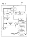
- FIG. 2 depicts an apparatus adapted for facilitating error detection for CAM in accordance with an embodiment of the disclosures made herein.
- CAM error detection methods and disclosed CAM error detection apparatuses, respectively, which provide corresponding disclosed CAM error detection functionality.
- Conventional CAM modules are defined herein to include off-the-shelf CAM modules that are not specially configured or specifically configured for facilitating error detection of a CAM module storage array, a CAM module input bus and/or a CAM module output bus.
- Disclosed CAM error detection methods and disclosed CAM error detection apparatuses provide CAM error detection functionality for the CAM module storage array, the CAM module input bus and the CAM module output bus. Providing error detection on input data and output data of conventional CAM modules is more cost-effective than designing and implementing non-conventional CAM modules, particularly when means for providing such disclosed CAM error detection functionality is less costly than implementing non-conventional CAM modules.
- disclosed CAM error detection functionality enables conventional CAM modules to be used for Connection Identifier (CI) compression in a manner that meets requirements of carrier-class ATM switches. Because disclosed CAM error detection functionality enables carrier-class ATM switches to be manufactured with conventional CAM modules, which are cost-effective, switches incorporating disclosed methods and/or disclosed apparatuses are advantageous with respect to cost and performance of conventional switches. Hence, the competitiveness of ATM switches incorporating disclosed CAM error detection functionality is improved.
- CI Connection Identifier
- FIG. 1 depicts a method 100 adapted for facilitating data error detection for CAM modules in accordance with an embodiment of the disclosures made herein.
- An operation 102 is performed for generating a parity word based on a key (i.e., key-based parity word).
- the key is received from a requesting system entity.
- the parity word comprises one or more bits.
- the value of the one or more bits is a function of the key.
- the parity word may be obtained using known err or detection techniques (e.g., cyclical redundancy check, bit interleaved parity generating, etc.)
- a 28-bit VPI/VCI word is an example of a basis for the key in ATM applications.
- the key and the key-based parity word jointly define a comparand.
- an operation 104 is performed for searching storage of a CAM module for an address containing data corresponding to the comparand after the comparand is provided to the CAM module. If a data error (e.g., a bit error) has occurred anywhere in the comparand, an address containing data corresponding to the comparand will not be found in the storage of the CAM module.
- an operation 106 is performed for issuing an input error indication.
- the input error indication means that a data error has occurred somewhere in the comparand, or that the original key was not found in the CAM.
- an operation 108 is performed for accessing a predetermined protection word that corresponds to the address containing data corresponding to the comparand.
- Searching memory including a plurality of predetermined protection words and finding the predetermined protection word is an example of accessing the predetermined protection word.
- an operation 110 is performed for generating a protection word based on the key (i.e., key-based protection word).
- an operation 112 is performed for comparing the predetermined protection word with the key-based protection word.
- an operation 114 is performed for facilitating (e.g., issuing) an output error indication.
- the output error indication means that the address from the CAM has not accessed a matching protection word in the memory and, hence, the address is corrupt.
- an operation 116 is performed for providing the address to the requesting system entity.
- An input error detection process for detecting errors on an input bus on a CAM module comprises generating the key-based parity word, searching storage of the CAM module and issuing the input error indication.
- An output error detection process for detecting errors on an output bus of a CAM module comprises accessing the predetermined protection word, generating the protection word based on the key (i.e., key-based protection word), comparing the predetermined protection word with the key-based protection word and issuing the output error indication.
- FIG. 2 depicts an embodiment of an apparatus 200 capable of carrying out the method 100 of FIG. 1.
- An ATM switch is an example of the apparatus 200. Carrying out the method 100 via the apparatus 200 enables CAM error detection functionality in accordance with an embodiment of the disclosures made herein.
- the apparatus 200 includes a Connection Manager (CM) 202 connected to a CAM module 204.
- the CM 202 includes a parity word generator 206, a protection word generator 208, memory 210 and a comparator 212.
- the CAM module 204 includes a storage array 214.
- the parity word generator 206 is connected to the storage array 214.
- the protection word generator 208 and the memory 210 are connected to inputs of the comparator 212.
- the memory 210 is connected between the output of the storage array 214 and one of the inputs of the comparator 212.
- the parity word generator 206 is adapted for generating a parity word upon being provided a key 216 (i.e., a key-based parity word 218).
- the key-based parity word 218 and the key 216 jointly define a comparand, which is provided to the storage array 214 of the CAM module 204.
- the storage array 214 of the CAM module 204 is searched in an attempt to access an address 220 containing data that corresponds to the comparand.
- An appropriate portion of the CAM module 204 provides an error notification 222 to the CM 202 if a data error (e.g., a bit error) has occurred in the comparand.
- a data error in the comparand prevents the address 220 containing data that corresponds to the comparand from being accessed in the storage array 214 of the CAM module 204.
- the error notification 222 is provided to the CM 202 for enabling an input error indication 224 to be issued.
- An input error detection module comprises the parity word generator 206 and means (not specifically shown) of the CM 202 adapted for issuing the input error indication 224.
- the protection word generator 208 generates a protection word from the key 216 (i.e., a key-based protection word 226).
- a device capable of generating a cyclical redundancy code or a bit interleaved parity word is an example of the protection word generator 208.
- a plurality of predetermined protection words (e.g., 4 bit protection words) is stored in the memory 210 of the CM 202.
- the memory 210 of the CM 202 is searched for accessing a predetermined protection word 228 corresponding to the address 220 assessed from the storage array 214 of the CAM module 204.
- the comparator 212 compares the key-based protection word 226 with the predetermined protection word 228.
- the key-based protection word 226 is different than predetermined protection word 228 (i.e., when inputs of the comparator 208 are not equal)
- the address 220 from the CAM module 204 has not accessed a matching predetermined protection word in the memory 210.
- the address 220 is corrupt and the comparator 212 facilitates issuance of an output error indication 230.
- An input error detection module capable of detecting errors on an input bus on a CAM module comprises the parity word generator 206 and means (not shown) of the CM 202 adapted for issuing the input error indication 224.
- An output error detection module capable of detecting errors on an output bus on a CAM module comprises the protection word generator 208, the memory 210 and the comparator 212.
- a data processor program in accordance with an embodiment of the disclosures made herein controls at least a portion of the operations associated with facilitating disclosed CAM error detection functionality.
- Such a data processor program is processible by a data processor of an apparatus in accordance with an embodiment of the disclosures made herein for carrying out operations of a method in accordance with an embodiment of the disclosures made herein.
- a data processor program may be resident on one or more data processing modules (e.g. a card including the data processor) or may be accessible by the data processor from an apparatus such as a diskette, a compact disk, a network storage device, a component of the network system or other suitable apparatus.
- the term data processor program refers to computer software, data processor algorithms or any other type of/sets of instruction code capable of controlling operations associated with a data processor.
- a microprocessor an application specific integrated circuit (ASIC), a field-programmable gate array (FPGA) and other types of programmable logic devices (PLDs) are examples of data processors capable of facilitating disclosed CAM error detection functionality.
- ASIC application specific integrated circuit
- FPGA field-programmable gate array
- PLDs programmable logic devices
- a FPGA may be used to generate parity and protection words, with appropriate software being used to configure the FPGA appropriately and to report any detected errors.
- a data processor program accessible from an apparatus by a data processor is defined herein as a data processor program product.
- a read-only memory (ROM), a programmable read-only memory (PROM), an erasable programmable read-only memory (EPROM), an electrically erasable programmable read-only memory (EEPROM), an electrically alterable programmable read-only memory (EAPROM), a flash memory, other non-volatile memory (NVM), a compact disk (CD/CDR/CDRW), or a digital video disk (DVD/DVDR/DVDRW) having a data processor program adapted for carrying out disclosed CAM error detection functionality are examples of a data processor program product.
Landscapes
- Engineering & Computer Science (AREA)
- Theoretical Computer Science (AREA)
- Quality & Reliability (AREA)
- Physics & Mathematics (AREA)
- General Engineering & Computer Science (AREA)
- General Physics & Mathematics (AREA)
- Detection And Correction Of Errors (AREA)
- Storage Device Security (AREA)
- Techniques For Improving Reliability Of Storages (AREA)
Applications Claiming Priority (2)
| Application Number | Priority Date | Filing Date | Title |
|---|---|---|---|
| US10/663,612 US7296210B2 (en) | 2003-09-16 | 2003-09-16 | Facilitating error detection for content addressable memory |
| US663612 | 2003-09-16 |
Publications (2)
| Publication Number | Publication Date |
|---|---|
| EP1517336A2 true EP1517336A2 (de) | 2005-03-23 |
| EP1517336A3 EP1517336A3 (de) | 2008-04-09 |
Family
ID=34194726
Family Applications (1)
| Application Number | Title | Priority Date | Filing Date |
|---|---|---|---|
| EP04300594A Withdrawn EP1517336A3 (de) | 2003-09-16 | 2004-09-10 | Verfahren zur Erleichterung der Fehlererkennung für inhaltsadressierbare Speicher |
Country Status (2)
| Country | Link |
|---|---|
| US (1) | US7296210B2 (de) |
| EP (1) | EP1517336A3 (de) |
Cited By (1)
| Publication number | Priority date | Publication date | Assignee | Title |
|---|---|---|---|---|
| US7254748B1 (en) * | 2003-10-14 | 2007-08-07 | Netlogic Microsystems, Inc. | Error correcting content addressable memory |
Families Citing this family (10)
| Publication number | Priority date | Publication date | Assignee | Title |
|---|---|---|---|---|
| US7301961B1 (en) | 2001-12-27 | 2007-11-27 | Cypress Semiconductor Corportion | Method and apparatus for configuring signal lines according to idle codes |
| US7761774B2 (en) * | 2005-10-28 | 2010-07-20 | Qualcomm Incorporated | High speed CAM lookup using stored encoded key |
| US7752492B1 (en) * | 2007-05-25 | 2010-07-06 | Emc Corporation | Responding to a failure of a storage system |
| US8533578B2 (en) | 2010-06-11 | 2013-09-10 | Freescale Semiconductor, Inc. | Error detection in a content addressable memory (CAM) and method of operation |
| US20120110411A1 (en) * | 2010-10-29 | 2012-05-03 | Brocade Communications Systems, Inc. | Content Addressable Memory (CAM) Parity And Error Correction Code (ECC) Protection |
| KR20130093707A (ko) * | 2011-12-23 | 2013-08-23 | 한국전자통신연구원 | 패킷 분류 장치 및 그것의 패킷 분류 방법 |
| US9170880B1 (en) * | 2013-10-08 | 2015-10-27 | Qlogic, Corporation | Method and system for data integrity in TCAMS |
| US9411600B2 (en) * | 2013-12-08 | 2016-08-09 | Intel Corporation | Instructions and logic to provide memory access key protection functionality |
| KR102675508B1 (ko) * | 2020-03-17 | 2024-06-17 | 에스케이하이닉스 주식회사 | 메모리 장치 및 이의 동작 방법 |
| US12142334B2 (en) * | 2021-05-04 | 2024-11-12 | Micron Technology, Inc. | Health scan for content addressable memory |
Family Cites Families (7)
| Publication number | Priority date | Publication date | Assignee | Title |
|---|---|---|---|---|
| US6067656A (en) * | 1997-12-05 | 2000-05-23 | Intel Corporation | Method and apparatus for detecting soft errors in content addressable memory arrays |
| US6597595B1 (en) * | 2001-08-03 | 2003-07-22 | Netlogic Microsystems, Inc. | Content addressable memory with error detection signaling |
| US7002823B1 (en) * | 2001-08-03 | 2006-02-21 | Netlogic Microsystems, Inc. | Content addressable memory with simultaneous write and compare function |
| US6914795B1 (en) * | 2001-08-03 | 2005-07-05 | Netlogic Microsystems, Inc. | Content addressable memory with selective error logging |
| US6978343B1 (en) * | 2002-08-05 | 2005-12-20 | Netlogic Microsystems, Inc. | Error-correcting content addressable memory |
| US6947301B2 (en) * | 2002-12-24 | 2005-09-20 | Micron Technology, Inc. | Content addressable memory (CAM) device employing a recirculating shift register for data storage |
| US6944039B1 (en) * | 2003-12-12 | 2005-09-13 | Netlogic Microsystems, Inc. | Content addressable memory with mode-selectable match detect timing |
-
2003
- 2003-09-16 US US10/663,612 patent/US7296210B2/en not_active Expired - Fee Related
-
2004
- 2004-09-10 EP EP04300594A patent/EP1517336A3/de not_active Withdrawn
Cited By (1)
| Publication number | Priority date | Publication date | Assignee | Title |
|---|---|---|---|---|
| US7254748B1 (en) * | 2003-10-14 | 2007-08-07 | Netlogic Microsystems, Inc. | Error correcting content addressable memory |
Also Published As
| Publication number | Publication date |
|---|---|
| US7296210B2 (en) | 2007-11-13 |
| US20050060631A1 (en) | 2005-03-17 |
| EP1517336A3 (de) | 2008-04-09 |
Similar Documents
| Publication | Publication Date | Title |
|---|---|---|
| US7143251B1 (en) | Data storage using identifiers | |
| US8122319B2 (en) | Page-based failure management for flash memory | |
| US7296210B2 (en) | Facilitating error detection for content addressable memory | |
| US6041001A (en) | Method of increasing data reliability of a flash memory device without compromising compatibility | |
| US7240178B2 (en) | Non-volatile memory and non-volatile memory data rewriting method | |
| EP2014054B1 (de) | Verfahren und vorrichtung für approximativen strukturabgleich | |
| US20050289295A1 (en) | Error Protection For Lookup Operations in Content-Addressable Memory Entries | |
| US20060069851A1 (en) | Integrated circuit memory devices that support detection of write errors occuring during power failures and methods of operating same | |
| EP1634198A1 (de) | Verfahren und system zum vergleich von datenbytes mit gespeicherten zeichenkettensegmenten | |
| JP2004054935A (ja) | マスク可能な内容照合メモリにおけるビットエラーの検出方法および装置 | |
| US20100058144A1 (en) | Memory system with ecc-unit and further processing arrangement | |
| US10366773B2 (en) | E-fuse circuit | |
| US10971246B2 (en) | Performing error correction in computer memory | |
| US20060120166A1 (en) | Data processing apparatus and method for flash memory | |
| CN108074620B (zh) | 修复控制器件及包括其的半导体器件 | |
| US7305519B1 (en) | Error protection for associative memory entries and lookup operations performed thereon | |
| US7788550B2 (en) | Redundant bit patterns for column defects coding | |
| US7213191B2 (en) | System and method for securely storing data in a memory | |
| WO2003003258A2 (en) | I.c. cell and library identification | |
| US8020115B2 (en) | Apparatus, method and system for permanent storage of data | |
| US9529669B2 (en) | Error detection and correction in binary content addressable memory (BCAM) | |
| US7345897B2 (en) | Error protected ternary content-addressable memories and lookup operations performed thereon | |
| EP1402365A1 (de) | Verfahren und schaltungsanordnung zur speicherfehlerverarbeitung | |
| US20070088909A1 (en) | Identifying content-addressable memory entries differing from a lookup word in multiple but less than a predetermined number of bit positions | |
| US8028221B2 (en) | Error correction and error detection method for reading of stored information data and a storage control unit for the same |
Legal Events
| Date | Code | Title | Description |
|---|---|---|---|
| PUAI | Public reference made under article 153(3) epc to a published international application that has entered the european phase |
Free format text: ORIGINAL CODE: 0009012 |
|
| AK | Designated contracting states |
Kind code of ref document: A2 Designated state(s): AT BE BG CH CY CZ DE DK EE ES FI FR GB GR HU IE IT LI LU MC NL PL PT RO SE SI SK TR |
|
| AX | Request for extension of the european patent |
Extension state: AL HR LT LV MK |
|
| RAP1 | Party data changed (applicant data changed or rights of an application transferred) |
Owner name: ALCATEL LUCENT |
|
| PUAL | Search report despatched |
Free format text: ORIGINAL CODE: 0009013 |
|
| AK | Designated contracting states |
Kind code of ref document: A3 Designated state(s): AT BE BG CH CY CZ DE DK EE ES FI FR GB GR HU IE IT LI LU MC NL PL PT RO SE SI SK TR |
|
| AX | Request for extension of the european patent |
Extension state: AL HR LT LV MK |
|
| 17P | Request for examination filed |
Effective date: 20081009 |
|
| AKX | Designation fees paid |
Designated state(s): AT BE BG CH CY CZ DE DK EE ES FI FR GB GR HU IE IT LI LU MC NL PL PT RO SE SI SK TR |
|
| RAP1 | Party data changed (applicant data changed or rights of an application transferred) |
Owner name: ALCATEL LUCENT |
|
| 111Z | Information provided on other rights and legal means of execution |
Free format text: AT BE BG CH CY CZ DE DK EE ES FI FR GB GR HU IE IT LI LU MC NL PL PT RO SE SI SK TR Effective date: 20130410 |
|
| 17Q | First examination report despatched |
Effective date: 20140116 |
|
| RAP1 | Party data changed (applicant data changed or rights of an application transferred) |
Owner name: ALCATEL LUCENT |
|
| D11X | Information provided on other rights and legal means of execution (deleted) | ||
| STAA | Information on the status of an ep patent application or granted ep patent |
Free format text: STATUS: THE APPLICATION IS DEEMED TO BE WITHDRAWN |
|
| 18D | Application deemed to be withdrawn |
Effective date: 20160401 |