EP1517243A2 - Memory interleave system - Google Patents
Memory interleave system Download PDFInfo
- Publication number
- EP1517243A2 EP1517243A2 EP04021718A EP04021718A EP1517243A2 EP 1517243 A2 EP1517243 A2 EP 1517243A2 EP 04021718 A EP04021718 A EP 04021718A EP 04021718 A EP04021718 A EP 04021718A EP 1517243 A2 EP1517243 A2 EP 1517243A2
- Authority
- EP
- European Patent Office
- Prior art keywords
- bank
- memory
- address
- intra
- bank address
- Prior art date
- Legal status (The legal status is an assumption and is not a legal conclusion. Google has not performed a legal analysis and makes no representation as to the accuracy of the status listed.)
- Withdrawn
Links
Images




Classifications
-
- G—PHYSICS
- G06—COMPUTING OR CALCULATING; COUNTING
- G06F—ELECTRIC DIGITAL DATA PROCESSING
- G06F12/00—Accessing, addressing or allocating within memory systems or architectures
- G06F12/02—Addressing or allocation; Relocation
- G06F12/06—Addressing a physical block of locations, e.g. base addressing, module addressing, memory dedication
- G06F12/0607—Interleaved addressing
-
- G—PHYSICS
- G11—INFORMATION STORAGE
- G11C—STATIC STORES
- G11C8/00—Arrangements for selecting an address in a digital store
- G11C8/12—Group selection circuits, e.g. for memory block selection, chip selection, array selection
-
- G—PHYSICS
- G11—INFORMATION STORAGE
- G11C—STATIC STORES
- G11C7/00—Arrangements for writing information into, or reading information out from, a digital store
-
- G—PHYSICS
- G11—INFORMATION STORAGE
- G11C—STATIC STORES
- G11C8/00—Arrangements for selecting an address in a digital store
Definitions
- the present invention relates to a memory interleave system which realizes efficient memory access in a computer system.
- Fig. 6 shows an example of the arrangement of a conventional memory interleave system.
- the conventional memory interleave system shown in Fig. 6 is comprised of a vector computing unit (CPU) 101 which outputs eight vector elements V0 to V7, a leading element address, and an inter-element distance and generates a memory request for each vector element, a main storage unit 102 comprised of a plurality of memory banks 121, and a memory access control unit 103 which independently performs access control on each memory bank 121 between the vector computing unit 101 and the main storage unit 102 on the basis of a memory request.
- CPU vector computing unit
- main storage unit 102 comprised of a plurality of memory banks 121
- a memory access control unit 103 which independently performs access control on each memory bank 121 between the vector computing unit 101 and the main storage unit 102 on the basis of a memory request.
- the memory access control unit 103 further includes an adder unit 104, routing address generating unit 105, contention arbitration unit 106, and crossbar unit 107.
- the adder unit 104 adds the leading element address and inter-element distance sent from the vector computing unit 101 to generate the memory access address of a memory request for each vector element.
- the routing address generating unit 105 calculates the exclusive-OR between one bit of a routing address which is part of a memory access address and one bit other than the routing address of the memory access address for each vector element, and replaces one bit of the routing address with the resultant value, thereby generating a new routing address.
- the contention arbitration unit 106 performs contention arbitration between memory requests for each memory bank 121 in accordance with the new routing address.
- the crossbar unit 107 accesses the memory banks 121 in accordance with the contention arbitration.
- the bank interleave mode is made variable (for detailed information, see, for example, Japanese Patent Laid-Open No. 2002-342306).
- the conventional memory interleave system cannot improve deterioration in performance due to memory bank contention between the memory requests issued by a plurality of CPUs.
- a memory interleave system comprising M (M is 2 p 0 where p is a natural number) memory banks each including a plurality of memories, N (a natural number) computing means for outputting memory requests as access requests to the memory banks, the memory request containing a first bank address which is an address of the memory bank and a first intra-bank address which is an address of a memory in the memory bank, N address generating means respectively corresponding to the computing means, the address generating means receiving a memory request from the computing means, and newly generating and outputting a second intra-bank address and a second bank address by using the first intra-bank address and the first bank address which are contained in the memory request, and M memory control means respectively corresponding to the memory banks, the memory control means performing memory bank access control on the basis of the second intra-bank address output from the address generating means, and the memory control means which performs access control being selected on the basis of the second bank address output from the address generating means.
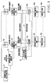
- Fig. 1 shows the arrangement of a memory interleave system according to the first embodiment of the present invention.
- the memory interleave system according to the first embodiment is comprised of N (a natural number) CPUs (computing means) 10 0 to 10 N-1 , a software visible register 11, N address generating units 12 0 to 12 N-1 connected to the CPUs 10 0 to 10 N-1 in a one-to-one correspondence, a select signal generating circuit 13, a crossbar unit 14 comprised of M (M is 2 p 0 where p is an integer equal to or more than two) selectors 14 0 to 14 M-1 , M memory control units 15 0 to 15 M-1 connected to the selectors 14 0 to 14 M-1 in a one-to-one correspondence, M memory banks 16 0 to 16 M-1 connected to the memory control units 15 0 to 15 M-1 in a one-to-one correspondence, and a memory bank allocating unit 17.
- N represents the number of connected CPUs (the number of input ports), and “M” represents the number of connected memory banks.
- p is an integer equal to or more than two. However, p may be one (i.e., p may be a natural number).
- Each of the memory banks 16 0 to 16 M-1 is an aggregate of a plurality of memories.
- the CPUs 10 0 to 10 N-1 issue memory requests which are access requests to the memory banks 16 0 to 16 M-1 .
- Each memory request includes the first bank address which is the address of a corresponding one of the memory banks 16 0 to 16 M-1 and the first intra-bank address which is the address of a corresponding one of the memories of a corresponding one of the memory banks 16 0 to 16 M-1 .
- a value indicating a bank interleave mode is set in the software visible register 11, which in turn notifies the memory bank allocating unit 17 of the set value.
- the software visible register 11 is comprised of flip-flops equal in number to bank interleave modes.
- flip-flops 11a, 11b, and 11c respectively correspond to an all bank interleave mode, 1/2 bank interleave mode, and 1/4 bank interleave mode.
- "1" is held in only a flip-flop corresponding to the mode to be used, and "0" is held in each remaining flip-flop.
- Each of the address generating units 12 0 to 12 N-1 receives a memory request from a corresponding one of the CPUs 10 0 to 10 N-1 , and newly generates the second intra-bank address and second bank address by using the first intra-bank address and first bank address contained in the memory request. That is, each of the address generating units 12 0 to 12 N-1 generates the second intra-bank address and second bank address by rearranging the first intra-bank address and first bank address for at least each 0 bit. In this case, "rearranging the first intra-bank address and first bank address for each 0 bit" means that the first intra-bank address and first bank address are set as the second intra-bank address and second bank address without rearrangement.
- each of the address generating units 12 0 to 12 N-1 generates, as the second intra-bank address, a bit string comprised of the (y - q) bits of the first intra-bank address (y bits) (excluding the upper q bits (q is an integer equal to or more than 0 and equal to or less than p)) contained in the memory request received from a corresponding one of the CPUs 10 0 to 10 N-1 and the upper q bits of the first bank address (x bits) contained in the memory request, and also generates, as the second bank address, a bit string comprised of the upper q bits of the first intra-bank address and the (x - q) bits of the first bank address excluding the upper q bits.
- the select signal generating circuit 13 receives the N second bank addresses output from the address generating units 12 0 to 12 N-1 .
- the select signal generating circuit 13 arbitrates the contention and outputs a select signal for selecting one memory bank 16 m (m is an integer satisfying 0 ⁇ m ⁇ M - 1) to the selector 14 m of the crossbar unit 14 which corresponds to the memory bank 16 m .
- the select signal generating circuit 13 selects one of them, and outputs a select signal to the selector 14 m of the crossbar unit 14 which corresponds to the memory bank 16 m of the selected second bank address.
- a method of determining one memory bank 16 m by assigning priorities to the memory banks 16 0 to 16 M-1 as access destinations is available.
- a general round-robin scheme, a fixed scheme, and the like are available as methods of assigning priorities to the memory banks 16 0 to 16 M-1 .
- the selectors 14 0 to 14 M-1 of the crossbar unit 14 receive the N second intra-bank addresses from the address generating units 12 0 to 12 N-1 and a select signal from the select signal generating circuit 13, and outputs one intra-bank address to a corresponding one of the memory control units 15 0 to 15 M-1 in accordance with the select signal.
- the memory control units 15 0 to 15 M-1 respectively perform access control on the corresponding memory banks 16 0 to 16 M-1 with the intra-bank addresses input from the selectors 14 0 to 14 M-1 .
- the memory banks 16 0 to 16 M-1 are formed into memory bank groups each including 1/2 q the total number of memory banks in accordance with the bank interleave mode setting value in the software visible register 11, and the respective memory bank groups can be simultaneously accessed. That is, the memory banks 16 0 to 16 M-1 can be interleaved into memory bank groups each including 1/2 q the total number of memory banks.
- the memory bank allocating unit 17 receives the bank interleave mode setting value notified from the software visible register 11, and controls the CPUs 10 0 to 10 N-1 in accordance with the setting value. More specifically, when the bank interleave mode setting value indicates the 1/2 q bank interleave mode, the memory banks 16 0 to 16 M-1 are interleaved into memory bank groups each including 1/2 q the total number of memory banks. Each of the memory bank groups is allocated to a corresponding one of the CPUs 10 0 to 10 N-1 to suppress the frequency of memory bank contention between the CPUs 10 0 to 10 N-1 .
- the memory bank allocating unit 17 limits at least one of the first intra-bank address and the first bank address, which can be output, depending on which memory bank groups are allocated to the respective CPUs 10 0 to 10 N-1 . In the first embodiment, the memory bank allocating unit 17 limits the first intra-bank address which can be output.
- the function of the memory bank allocating unit 17 can also be implemented by executing an operating system (OS) on the CPUs 10 0 to 10 N-1 .
- OS operating system
- a corresponding one of the address generating units 12 0 to 12 N-1 outputs the first intra-bank address (y bits) and first bank address (x bits) contained in the memory request received from each of the CPUs 10 0 to 10 N-1 as the second intra-bank address and second bank address without any change, as shown in Fig. 2B.
- each of the address generating units 12 0 to 12 N-1 When the setting value in the software visible register 11 indicates the 1/2 bank interleave mode, each of the address generating units 12 0 to 12 N-1 outputs, as the second intra-bank address, a bit string comprised of the (y - 1) bits of the first intra-bank address (excluding the most significant bit) contained in the memory request received from a corresponding one of the CPUs 10 0 to 10 N-1 and the most significant bit of the first bank address contained in the memory request, and also outputs, as the second bank address, a bit string comprised of the most significant bit of the first intra-bank address and the (x - 1) bits of the first bank address excluding the most significant bit, as shown in Fig. 2C.
- each of the address generating units 12 0 to 12 N-1 When the setting value in the software visible register 11 indicates the 1/4 bank interleave mode, each of the address generating units 12 0 to 12 N-1 outputs, as the second intra-bank address, a bit string comprised of the (y - 2) bits of the first intra-bank address (excluding the upper two bits) contained in the memory request received from a corresponding one of the CPUs 10 0 to 10 N-1 and the upper two bits of the first bank address contained in the memory request, and also outputs, as the second bank address, a bit string comprised of the upper two bits of the first intra-bank address and the (x - 2) bits of the first bank address excluding the upper two bits, as shown in Fig. 2D.
- the select signal generating circuit 13 outputs a select signal to the selector 14 m of the crossbar unit 14 which corresponds to one memory bank 16 m on the basis of the second bank address input from one of the address generating units 12 0 to 12 N-1 .
- the selector 14 m to which the select signal is input selects one intra-bank address and outputs it to the corresponding memory control unit 15 m .
- the memory control unit 15 m performs access control on the corresponding memory bank 16 m with the input intra-bank address.
- the memory bank allocating unit 17 allocates all the memory banks 16 0 to 16 M-1 to all the CPUs 10 0 to 10 N-1 to efficiently use them.
- the memory bank allocating unit 17 allocates a memory bank group (memory area) to each of the CPUs 10 0 to 10 N-1 . This makes it possible to suppress the frequency of memory bank contention between the CPU group which accesses the memory bank group (16 0 to 16 M/2-1 ) and the CPU group which accesses the memory bank group (16 M/2 to 16 M-1 ).
- the memory bank allocating unit 17 forms the N CPUs 10 0 to 10 N-1 into two or less groups (group a and group b), and allocates the memory areas of the memory bank group (16 0 to 16 M/2-1 ) to group a, and the memory areas of the memory bank group (16 M/2 to 16 M-1 ) to group b, thereby suppressing memory bank contention between group a and group b.
- the memory bank allocating unit 17 allocates a memory bank group (memory area) to each of the CPUs 10 0 to 10 N-1 .
- the memory bank allocating unit 17 forms the N CPUs 10 0 to 10 N-1 into four or less groups (group a, group b, group c, and group d), and allocates memory areas 0 to L/4 of the memory bank group (16 0 to 16 M/4-1 ) to group a, memory areas L/4 to L/2 of the memory bank group (16 M/4 to 16 M/2-1 ) to group b, memory areas L/2 to Lx3/4 of the memory bank group (16 M/2 to 16 3M/4-1 ) to group c, and memory areas Lx3/4 to L of the memory bank group (16 3M/4 to 16 M/-1 ) to group d, thereby suppressing memory bank contention between the respective CPU groups.
- the memory bank allocating unit 17 forms the CPUs 10 0 to 10 N-1 into 2 q or less groups in accordance with a memory interleave count 2 q of a bank interleave mode, and allocates a memory bank group (memory areas) including 1/2 q the total number of memory banks to each CPU group, thereby suppressing memory bank contention between the respective CPU groups:
- each intra-bank address is comprised of three bits
- each bank address is comprised of three bits.
- Figs. 3A and 3B explain examples of 64-word address mapping.
- the select signal generating circuit 13 receives the second bank addresses generated by the address generating units 12 0 to 12 7 corresponding to the CPUs 10 0 to 10 7 , arbitrates memory access contention, and outputs a select signal to the selector 14 m corresponding to a second bank address m.
- the selector 14 m to which the select signal is input selects the second intra-bank address to be output on the basis of the three bits of the select signal for selecting eight inputs.
- the selector 14 m when the three bits of the select signal are "000", the selector 14 m outputs the second intra-bank address from the address generating unit 12 0 corresponding to the CPU 10 0 . Likewise, when the three bits are "001”, the selector 14 m outputs the second intra-bank address from the address generating unit 12 1 corresponding to the CPU 10 1 . When the three bits are "010”, the selector 14 m outputs the second intra-bank address from the address generating unit 12 2 corresponding to the CPU 10 2 . When the three bits are "011”, the selector 14 m outputs the second intra-bank address from the address generating unit 12 3 corresponding to the CPU 10 3 .
- the selector 14 m When the three bits are "100”, the selector 14 m outputs the second intra-bank address from the address generating unit 12 4 corresponding to the CPU 10 4 . “hen the three bits are “101”, the selector 14 m outputs the second intra-bank address from the address generating unit 12 5 corresponding to the CPU 10 5 . When the three bits are "110”, the selector 14 m outputs the second intra-bank address from the address generating unit 12 6 corresponding to the CPU 10 6 . When the three bits are "111”, the selector 14 m outputs the second intra-bank address from the address generating unit 12 7 corresponding to the CPU 10 7 .
- the memory area is not divided.
- the addresses output from the CPUs 10 0 to 10 N-1 are translated into addresses like those shown in Table 1.
- the select signal generating circuit 13 receives the second bank addresses from the address generating units 12 0 to 12 N-1 and outputs a select signal to the selector 14 m . With this operation, the first half memory banks obtained by dividing the memory area into two areas are interleaved into the memory groups 16 0 to 16 3 , and the second half memory banks are interleaved into the memory bank groups 16 4 to 16 7 . As a consequence, the memory area is divided as shown in Fig. 3B.
- the addresses output from the CPUs 10 0 to 10 N-1 are translated into addresses like those shown in Table 1.
- the select signal generating circuit 13 receives the second bank addresses from the address generating units 12 0 to 12 N-1 and outputs a select signal to the selector 14 m .
- the memory area is divided into four areas with addresses 0 to 15 (each address indicating a logical word address), addresses 16 to 31, addresses 32 to 47, and addresses 48 to 63, and can be interleaved into memory banks 16 0 and 16 1 , memory banks 16 2 and 16 3 , memory banks 16 4 and 16 5 , and memory banks 16 6 and 16 7 .
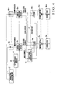
- Fig. 4 shows the arrangement of a memory interleave system according to the second embodiment of the present invention.
- a user application sets a value indicating a bank interleave mode in the software visible register 11. That is, the user application determines a bank interleave mode.
- a memory bank allocating unit 17 sets a value in a software visible register 11.
- the memory bank allocating unit 17 when assigning jobs to be executed to CPUs 10 0 to 10 N-1 , the memory bank allocating unit 17 itself determines a bank interleave mode by referring to the memory areas used by the CPUs 10 0 to 10 N-1 and the number of parallel operations by the CPUs 10 0 to 10 N-1 , and writes the corresponding value in the software visible register 11. This makes it possible to improve the utilization efficiency of the memories and the performance of the system.
- the function of the memory bank allocating unit 17 described above can be implemented by executing an operating system (OS) on the CPUs 10 0 to 10 N-1 .
- OS operating system
- Fig. 5 shows the arrangement of a memory interleave system according to the third embodiment of the present invention.
- a bank interleave mode is determined by setting a value indicating a bank interleave mode in the software visible register 11.
- a user determines a bank interleave mode by manually setting a value indicating a bank interleave mode with a hardware switch 21 such as a dip switch.
- the k-pole (k is a natural number) hardware switch 21 is prepared on a substrate, and a bank interleave mode is identified by the value set by the k-pole switch.
- the quadrupole hardware switch 21 Assume that the quadrupole hardware switch 21 is used. In this case, for example, when the value set by the hardware switch 21 is "0000", the all bank interleave mode is set. When the set value is "0001”, the 1/2 bank interleave mode is set. When the set value is "0010”, the 1/4 bank interleave mode is set. When the set value is "0011”, the 1/8 bank interleave mode is set.
- memory areas can be allocated to CPU groups, and memory bank contention between memory requests issued by the CPU groups can be reduced, and the utilization efficiency of the memories and the performance of the system can be improved.
Landscapes
- Engineering & Computer Science (AREA)
- Theoretical Computer Science (AREA)
- Physics & Mathematics (AREA)
- General Engineering & Computer Science (AREA)
- General Physics & Mathematics (AREA)
- Microelectronics & Electronic Packaging (AREA)
- Memory System (AREA)
- Dram (AREA)
- Techniques For Improving Reliability Of Storages (AREA)
Abstract
Description
| Logical Address | All Bank Interleave | 1/2 Bank Interleave | 1/4 Bank Interleave | ||||||
| Intra-bank | Bank | Physical | Intra-bank | Bank | Physical | Intra-bank | Bank | Physical | |
| AD | AD | AD | AD | AD | AD | AD | AD | AD | |
| 0 | 000 | 000 | 0 | 000 | 000 | 0 | 000 | 000 | 0 |
| 1 | 000 | 001 | 1 | 000 | 001 | 1 | 000 | 001 | 1 |
| 2 | 000 | 010 | 2 | 000 | 010 | 2 | 001 | 000 | 8 |
| 3 | 000 | 011 | 3 | 000 | 011 | 3 | 001 | 001 | 9 |
| 4 | 000 | 100 | 4 | 001 | 000 | 8 | 010 | 000 | 16 |
| 5 | 000 | 101 | 5 | 001 | 001 | 9 | 010 | 001 | 17 |
| 6 | 000 | 110 | 6 | 001 | 010 | 10 | 011 | 000 | 24 |
| 7 | 000 | 111 | 7 | 001 | 011 | 11 | 011 | 001 | 25 |
| 8 | 001 | 000 | 8 | 010 | 000 | 16 | 100 | 000 | 32 |
| 9 | 001 | 001 | 9 | 010 | 001 | 17 | 100 | 001 | 33 |
| 10 | 001 | 010 | 10 | 010 | 010 | 18 | 101 | 000 | 40 |
| 11 | 001 | 011 | 11 | 010 | 011 | 19 | 101 | 001 | 41 |
| 12 | 001 | 100 | 12 | 011 | 000 | 24 | 110 | 000 | 48 |
| 13 | 001 | 101 | 13 | 011 | 001 | 25 | 110 | 001 | 49 |
| 14 | 001 | 110 | 14 | 011 | 010 | 26 | 111 | 000 | 56 |
| 15 | 001 | 111 | 15 | 011 | 011 | 27 | 111 | 001 | 57 |
| 16 | 010 | 000 | 16 | 100 | 000 | 32 | 000 | 010 | 2 |
| 17 | 010 | 001 | 17 | 100 | 001 | 33 | 000 | 011 | 3 |
| 18 | 010 | 010 | 18 | 100 | 010 | 34 | 001 | 010 | 10 |
| 19 | 010 | 011 | 19 | 100 | 011 | 35 | 001 | 011 | 11 |
| 20 | 010 | 100 | 20 | 101 | 000 | 40 | 010 | 010 | 18 |
| 21 | 010 | 101 | 21 | 101 | 001 | 41 | 010 | 011 | 19 |
| 22 | 010 | 110 | 22 | 101 | 010 | 42 | 011 | 010 | 26 |
| 23 | 010 | 111 | 23 | 101 | 011 | 43 | 011 | 011 | 27 |
| 24 | 011 | 000 | 24 | 110 | 000 | 48 | 100 | 010 | 34 |
| 25 | 011 | 001 | 25 | 110 | 001 | 49 | 100 | 011 | 35 |
| 26 | 011 | 010 | 26 | 110 | 010 | 50 | 101 | 010 | 42 |
| 27 | 011 | 011 | 27 | 110 | 011 | 51 | 101 | 011 | 43 |
| 28 | 011 | 100 | 28 | 111 | 000 | 56 | 110 | 010 | 50 |
| 29 | 011 | 101 | 29 | 111 | 001 | 57 | 110 | 011 | 51 |
| 30 | 011 | 110 | 30 | 111 | 010 | 58 | 111 | 010 | 58 |
| 31 | 011 | 111 | 31 | 111 | 011 | 59 | 111 | 011 | 59 |
| 32 | 100 | 000 | 32 | 000 | 100 | 4 | 000 | 100 | 4 |
| 33 | 100 | 001 | 33 | 000 | 101 | 5 | 000 | 101 | 5 |
| 34 | 100 | 010 | 34 | 000 | 110 | 6 | 001 | 100 | 12 |
| 35 | 100 | 011 | 35 | 000 | 111 | 7 | 001 | 101 | 13 |
| 36 | 100 | 100 | 36 | 001 | 100 | 12 | 010 | 100 | 20 |
| 37 | 100 | 101 | 37 | 001 | 101 | 13 | 010 | 101 | 21 |
| 38 | 100 | 110 | 38 | 001 | 110 | 14 | 011 | 100 | 28 |
| 39 | 100 | 111 | 39 | 001 | 111 | 15 | 011 | 101 | 29 |
| 40 | 101 | 000 | 40 | 010 | 100 | 20 | 100 | 100 | 36 |
| 41 | 101 | 001 | 41 | 010 | 101 | 21 | 100 | 101 | 37 |
| 42 | 101 | 010 | 42 | 010 | 110 | 22 | 101 | 100 | 44 |
| 43 | 101 | 011 | 43 | 010 | 111 | 23 | 101 | 101 | 45 |
| 44 | 101 | 100 | 44 | 011 | 100 | 28 | 110 | 100 | 52 |
| 45 | 101 | 101 | 45 | 011 | 101 | 29 | 110 | 101 | 53 |
| 46 | 101 | 110 | 46 | 011 | 110 | 30 | 111 | 100 | 60 |
| 47 | 101 | 111 | 47 | 011 | 111 | 31 | 111 | 101 | 61 |
| 48 | 110 | 000 | 48 | 100 | 100 | 36 | 000 | 110 | 6 |
| 49 | 110 | 001 | 49 | 100 | 101 | 37 | 000 | 111 | 7 |
| 50 | 110 | 010 | 50 | 100 | 110 | 38 | 001 | 110 | 14 |
| 51 | 110 | 011 | 51 | 100 | 111 | 39 | 001 | 111 | 15 |
| 52 | 110 | 100 | 52 | 101 | 100 | 44 | 010 | 110 | 22 |
| 53 | 110 | 101 | 53 | 101 | 101 | 45 | 010 | 111 | 23 |
| 54 | 110 | 110 | 54 | 101 | 110 | 46 | 011 | 110 | 30 |
| 55 | 110 | 111 | 55 | 101 | 111 | 47 | 011 | 111 | 31 |
| 56 | 111 | 000 | 56 | 110 | 100 | 52 | 100 | 110 | 38 |
| 57 | 111 | 001 | 57 | 110 | 101 | 53 | 100 | 111 | 39 |
| 58 | 111 | 010 | 58 | 110 | 110 | 54 | 101 | 110 | 46 |
| 59 | 111 | 011 | 59 | 110 | 111 | 55 | 101 | 111 | 47 |
| 60 | 111 | 100 | 60 | 111 | 100 | 60 | 110 | 110 | 54 |
| 61 | 111 | 101 | 61 | 111 | 101 | 61 | 110 | 111 | 55 |
| 62 | 111 | 110 | 62 | 111 | 110 | 62 | 111 | 110 | 62 |
| 63 | 111 | 111 | 63 | 111 | 111 | 63 | 111 | 111 | 63 |
Claims (19)
- A memory interleave system characterized by comprising:M (M is 2p 0 where p is a natural number) memory banks (160 - 16M-1) each including a plurality of memories;N (a natural number) computing means (100 - 10N-1) for outputting memory requests as access requests to said memory banks, the memory request containing a first bank address which is an address of said memory bank and a first intra-bank address which is an address of a memory in said memory bank;N address generating means (120 - 12N-1) respectively corresponding to said computing means, said address generating means receiving a memory request from said computing means, and newly generating and outputting a second intra-bank address and a second bank address by using the first intra-bank address and the first bank address which are contained in the memory request; andM memory control means (150 - 15M-1) respectively corresponding to said memory banks, said memory control means performing memory bank access control on the basis of the second intra-bank address output from said address generating means, and said memory control means which is to perform access control being selected on the basis of the second bank address output from said address generating means.
- A system according to claim 1, wherein said address generating means generates a second intra-bank address and a second bank address in accordance with a bank interleave mode setting value.
- A system according to claim 2, wherein said address generating means generates a second intra-bank address and a second bank address by rearranging the first intra-bank address and the first bank address for at least 0 bit in accordance with the bank interleave mode setting value.
- A system according to claim 3, wherein when the bank interleave mode setting value indicates a 1/2q bank interleave mode (q is an integer of not less than 0 and not more than p) and a first bank address and a first intra-bank address respectively include x bits and y bits (x and y are integers of not less than q), said address generating means sets, as a second intra-bank address, a bit string comprised of (y - q) bits of the first intra-bank address excluding upper q bits and upper q bits of the first bank address, and also sets, as a second bank address, a bit string comprised of the upper q bits of the first intra-bank address and (x - q) bits of the first bank address excluding the upper q bits.
- A system according to claim 4, wherein
said address generating means sets the first intra-bank address and the first bank address as a second intra-bank address and a second bank address, respectively, without any change when the bank interleave mode setting value indicates an all bank interleave mode,
sets, as a second intra-bank address, a bit string comprised of (y - 1) bits of the first intra-bank address excluding a most significant bit and a most significant bit of the first bank address, and also sets, as a second bank address, a bit string comprised of the most significant bit of the first intra-bank address and (x - 1) bits of the first bank address excluding the most significant bit when the bank interleave mode setting value indicates a 1/2 bank interleave mode, and
sets, as a second intra-bank address, a bit string comprised of upper two bits of the first bank address and (y - 2) bits of the first intra-bank address excluding upper two bits, and also sets, as a second bank address, a bit string comprised of the two upper bits of the first intra-bank address and (x - 2) bits of the first bank address excluding the upper two bits when the bank interleave mode setting value indicates a 1/4 bank interleave mode. - A system according to claim 1, further comprising
M selectors (140 - 14M-1) respectively corresponding to said memory control means, said selectors receiving N second intra-bank addresses from said address generating means and a select signal, and outputting an intra-bank address to said memory control means in accordance with the select signal, and
select signal generating means (13) for receiving N second bank addresses from said address generating means, selecting one of a plurality of second bank addresses when the plurality of second bank addresses contend, and outputting a select signal to said selector corresponding to said memory bank of the selected second bank address. - A system according to claim 2, further comprising a software visible register (11) in which a bank interleave mode setting value is set in a software manner and which outputs the setting value to said address generating means.
- A system according to claim 7, wherein said software visible register allows a user application to variably set a bank interleave mode setting value.
- A system according to claim 7, further comprising memory bank allocating means (17) for receiving the bank interleave mode setting value output from said software visible register and controlling said computing means in accordance with the setting value.
- A system according to claim 9, wherein when the bank interleave mode setting value indicates a 1/2q bank interleave mode (q is an integer of not less than 0 and not more than p), said memory bank allocating means forms said M memory banks into 2q memory bank groups, and allocates one of the memory bank groups to each of said computing means.
- A system according to claim 10, wherein said memory bank allocating means limits at least one of a first intra-bank address and a first bank address which can be output to said computing means depending on which memory bank group is allocated to said computing means.
- A system according to claim 9, wherein said software visible register allows said memory bank allocating means to variably set a bank interleave mode setting value.
- A system according to claim 2, further comprising a hardware switch (21) which allows a bank interleave mode setting value to be manually set and outputs the setting value to said address generating means.
- A system according to claim 13, further comprising memory bank allocating means (17) for receiving the bank interleave mode setting value output from said hardware switch and controlling said computing means in accordance with the setting value.
- A system according to claim 14, wherein when the bank interleave mode setting value indicates a 1/2q bank interleave mode (q is an integer of not less than 0 and not more than p), said memory bank allocating means forms said M memory banks into 2q memory bank groups, and allocates one of the memory bank groups to each of said computing means.
- A system according to claim 15, wherein said memory bank allocating means limits at least one of a first intra-bank address and a first bank address which can be output to said computing means depending on which memory bank group is allocated to said computing means.
- A system according to claim 1, wherein N is an integer of not less than two.
- A system according to claim 1, wherein said computing means comprises a CPU (Central Processing Unit).
- A system according to claim 1, wherein said M selectors constitute crossbar means.
Applications Claiming Priority (2)
| Application Number | Priority Date | Filing Date | Title |
|---|---|---|---|
| JP2003322342A JP3950831B2 (en) | 2003-09-16 | 2003-09-16 | Memory interleaving method |
| JP2003322342 | 2003-09-16 |
Publications (2)
| Publication Number | Publication Date |
|---|---|
| EP1517243A2 true EP1517243A2 (en) | 2005-03-23 |
| EP1517243A3 EP1517243A3 (en) | 2006-01-04 |
Family
ID=34191270
Family Applications (1)
| Application Number | Title | Priority Date | Filing Date |
|---|---|---|---|
| EP04021718A Withdrawn EP1517243A3 (en) | 2003-09-16 | 2004-09-13 | Memory interleave system |
Country Status (7)
| Country | Link |
|---|---|
| US (1) | US7346750B2 (en) |
| EP (1) | EP1517243A3 (en) |
| JP (1) | JP3950831B2 (en) |
| KR (1) | KR100640704B1 (en) |
| AU (1) | AU2004210521B2 (en) |
| BR (1) | BRPI0403984A (en) |
| CA (1) | CA2480841A1 (en) |
Cited By (3)
| Publication number | Priority date | Publication date | Assignee | Title |
|---|---|---|---|---|
| WO2009056080A3 (en) * | 2007-10-31 | 2009-09-03 | Valasek Josef | Direct access memory constitution and the direct access memory device |
| WO2012074998A1 (en) | 2010-12-02 | 2012-06-07 | Advanced Micro Devices, Inc. | Partitioning of memory device for multi-client computing system |
| US10241687B2 (en) | 2015-04-14 | 2019-03-26 | Samsung Electronics Co., Ltd. | Method for operating semiconductor device and semiconductor system |
Families Citing this family (23)
| Publication number | Priority date | Publication date | Assignee | Title |
|---|---|---|---|---|
| US8250295B2 (en) * | 2004-01-05 | 2012-08-21 | Smart Modular Technologies, Inc. | Multi-rank memory module that emulates a memory module having a different number of ranks |
| US7289386B2 (en) | 2004-03-05 | 2007-10-30 | Netlist, Inc. | Memory module decoder |
| US7916574B1 (en) | 2004-03-05 | 2011-03-29 | Netlist, Inc. | Circuit providing load isolation and memory domain translation for memory module |
| US7532537B2 (en) * | 2004-03-05 | 2009-05-12 | Netlist, Inc. | Memory module with a circuit providing load isolation and memory domain translation |
| JP4288421B2 (en) * | 2004-03-12 | 2009-07-01 | 日本電気株式会社 | Main storage system and main storage device for controlling correspondence with CPU |
| JP5055989B2 (en) * | 2006-12-08 | 2012-10-24 | 富士通セミコンダクター株式会社 | Memory controller |
| TWM326186U (en) * | 2007-06-13 | 2008-01-21 | Princeton Technology Corp | Device for data be written into memory |
| US8417870B2 (en) * | 2009-07-16 | 2013-04-09 | Netlist, Inc. | System and method of increasing addressable memory space on a memory board |
| US8154901B1 (en) | 2008-04-14 | 2012-04-10 | Netlist, Inc. | Circuit providing load isolation and noise reduction |
| US8516185B2 (en) | 2009-07-16 | 2013-08-20 | Netlist, Inc. | System and method utilizing distributed byte-wise buffers on a memory module |
| JP5365336B2 (en) * | 2009-05-01 | 2013-12-11 | ソニー株式会社 | Memory control device and memory control method |
| US9128632B2 (en) | 2009-07-16 | 2015-09-08 | Netlist, Inc. | Memory module with distributed data buffers and method of operation |
| KR101553651B1 (en) | 2009-10-13 | 2015-09-17 | 삼성전자 주식회사 | apparatus for accessing multi-bank memory |
| KR101620460B1 (en) | 2010-05-04 | 2016-05-13 | 삼성전자주식회사 | Interconnect, bus system having interconnect and operating method of bus system |
| KR101673233B1 (en) | 2010-05-11 | 2016-11-17 | 삼성전자주식회사 | Transection splitting apparatus and method |
| US8380940B2 (en) * | 2010-06-25 | 2013-02-19 | Qualcomm Incorporated | Multi-channel multi-port memory |
| CN110428855B (en) | 2013-07-27 | 2023-09-22 | 奈特力斯股份有限公司 | Memory modules with local separately synchronized |
| JP2016218721A (en) * | 2015-05-20 | 2016-12-22 | ソニー株式会社 | Memory control circuit and memory control method |
| JP2017156948A (en) * | 2016-03-01 | 2017-09-07 | ソニー株式会社 | MEMORY CONTROL DEVICE, MEMORY DEVICE, INFORMATION PROCESSING SYSTEM, AND MEMORY CONTROL METHOD |
| US10366005B2 (en) * | 2016-05-20 | 2019-07-30 | Nxp Usa, Inc. | Memory interleave system and method therefor |
| US11663043B2 (en) | 2019-12-02 | 2023-05-30 | Meta Platforms, Inc. | High bandwidth memory system with dynamically programmable distribution scheme |
| US11429523B2 (en) | 2020-05-15 | 2022-08-30 | Microsoft Technology Licensing, Llc | Two-way interleaving in a three-rank environment |
| US12596641B2 (en) | 2024-01-29 | 2026-04-07 | Qualcomm Incorporated | Hardware and software hybrid configuration of DRAM channel interleaving management |
Family Cites Families (12)
| Publication number | Priority date | Publication date | Assignee | Title |
|---|---|---|---|---|
| JPS5128450B2 (en) | 1971-10-06 | 1976-08-19 | ||
| JPS5619575A (en) * | 1979-07-25 | 1981-02-24 | Fujitsu Ltd | Data processing system having hierarchy memory |
| JPS58149551A (en) | 1982-02-27 | 1983-09-05 | Fujitsu Ltd | Storage controlling system |
| JPS58154059A (en) | 1982-03-08 | 1983-09-13 | Omron Tateisi Electronics Co | Memory access system of parallel processing system |
| US5392443A (en) * | 1991-03-19 | 1995-02-21 | Hitachi, Ltd. | Vector processor with a memory assigned with skewed addresses adapted for concurrent fetching of a number of vector elements belonging to the same vector data |
| CA2138263C (en) | 1993-09-27 | 2000-02-22 | Yukihiko Okumura | Multiprocessor |
| JPH10301842A (en) * | 1997-04-25 | 1998-11-13 | Nec Corp | Memory controller |
| DE69912478T2 (en) | 1998-12-18 | 2004-08-19 | Unisys Corp. | STORAGE ADDRESS TRANSLATION ARRANGEMENT AND METHOD FOR A STORAGE WITH SEVERAL STORAGE UNITS |
| US6453380B1 (en) * | 1999-01-23 | 2002-09-17 | International Business Machines Corporation | Address mapping for configurable memory system |
| US6233662B1 (en) | 1999-04-26 | 2001-05-15 | Hewlett-Packard Company | Method and apparatus for interleaving memory across computer memory banks |
| JP3789316B2 (en) | 2001-05-15 | 2006-06-21 | エヌイーシーコンピュータテクノ株式会社 | Routing address generation method for vector processor |
| US6912616B2 (en) * | 2002-11-12 | 2005-06-28 | Hewlett-Packard Development Company, L.P. | Mapping addresses to memory banks based on at least one mathematical relationship |
-
2003
- 2003-09-16 JP JP2003322342A patent/JP3950831B2/en not_active Expired - Fee Related
-
2004
- 2004-09-08 AU AU2004210521A patent/AU2004210521B2/en not_active Ceased
- 2004-09-09 CA CA002480841A patent/CA2480841A1/en not_active Abandoned
- 2004-09-13 EP EP04021718A patent/EP1517243A3/en not_active Withdrawn
- 2004-09-13 US US10/938,627 patent/US7346750B2/en not_active Expired - Fee Related
- 2004-09-13 KR KR1020040073076A patent/KR100640704B1/en not_active Expired - Fee Related
- 2004-09-16 BR BR0403984-0A patent/BRPI0403984A/en not_active IP Right Cessation
Cited By (5)
| Publication number | Priority date | Publication date | Assignee | Title |
|---|---|---|---|---|
| WO2009056080A3 (en) * | 2007-10-31 | 2009-09-03 | Valasek Josef | Direct access memory constitution and the direct access memory device |
| US8271699B2 (en) | 2007-10-31 | 2012-09-18 | Josef Valasek | Parallel accessible memory system enabling the simultaneous access to bytes of data |
| WO2012074998A1 (en) | 2010-12-02 | 2012-06-07 | Advanced Micro Devices, Inc. | Partitioning of memory device for multi-client computing system |
| CN103229157A (en) * | 2010-12-02 | 2013-07-31 | 超威半导体公司 | Partitioning of memory device for multi-client computing system |
| US10241687B2 (en) | 2015-04-14 | 2019-03-26 | Samsung Electronics Co., Ltd. | Method for operating semiconductor device and semiconductor system |
Also Published As
| Publication number | Publication date |
|---|---|
| KR20050027923A (en) | 2005-03-21 |
| US20050060482A1 (en) | 2005-03-17 |
| AU2004210521B2 (en) | 2009-01-08 |
| CA2480841A1 (en) | 2005-03-16 |
| JP3950831B2 (en) | 2007-08-01 |
| AU2004210521A1 (en) | 2005-04-07 |
| KR100640704B1 (en) | 2006-11-01 |
| JP2005092374A (en) | 2005-04-07 |
| US7346750B2 (en) | 2008-03-18 |
| BRPI0403984A (en) | 2005-05-24 |
| EP1517243A3 (en) | 2006-01-04 |
Similar Documents
| Publication | Publication Date | Title |
|---|---|---|
| US7346750B2 (en) | Memory interleave system | |
| US6185654B1 (en) | Phantom resource memory address mapping system | |
| KR910001736B1 (en) | Multiprocessing System | |
| EP0313788A2 (en) | An aperiodic mapping method to enhance power-of-two stride access to interleaved devices | |
| US5392443A (en) | Vector processor with a memory assigned with skewed addresses adapted for concurrent fetching of a number of vector elements belonging to the same vector data | |
| EP0424618A2 (en) | Input/output system | |
| EP1262878A2 (en) | Self-optimizing crossbar switch | |
| EP0503770A1 (en) | Interleaved multiprocessor memory system | |
| US6594718B1 (en) | Arbitration scheme for equitable distribution of bandwidth for agents with different bandwidth requirements | |
| US8868835B2 (en) | Cache control apparatus, and cache control method | |
| US5652861A (en) | System for interleaving memory modules and banks | |
| JP2004038959A (en) | Multiprocessor computer with shared program memory | |
| US6961804B2 (en) | Flexible techniques for associating cache memories with processors and main memory | |
| US11429452B2 (en) | Method for distributing keys using two auxiliary hashing functions | |
| CN105593832B (en) | Method and apparatus for use of memory regions that support interleaving | |
| JP4240610B2 (en) | Computer system | |
| US20030172245A1 (en) | Data processing method and device for parallel stride access | |
| JP2002342306A (en) | Routing address generating system for vector processor | |
| US20040111459A1 (en) | Methods and apparatus for modular reduction circuits | |
| JP4445708B2 (en) | How to access I/O modules using map tables | |
| US20230305881A1 (en) | Configurable Access to a Multi-Die Reconfigurable Processor by a Virtual Function | |
| EP0313787A2 (en) | A hardware mechanism for the dynamic customization of permutation using bit-matrix multiplication | |
| KR20240071396A (en) | Multipath memory with static or dynamic mapping to coherent or MMIO space | |
| US6144994A (en) | Interface for flexible address bandwidth allocation | |
| Yang et al. | High Throughput Matrix Transposition on HBM-Enabled FPGAs |
Legal Events
| Date | Code | Title | Description |
|---|---|---|---|
| PUAI | Public reference made under article 153(3) epc to a published international application that has entered the european phase |
Free format text: ORIGINAL CODE: 0009012 |
|
| AK | Designated contracting states |
Kind code of ref document: A2 Designated state(s): AT BE BG CH CY CZ DE DK EE ES FI FR GB GR HU IE IT LI LU MC NL PL PT RO SE SI SK TR |
|
| AX | Request for extension of the european patent |
Extension state: AL HR LT LV MK |
|
| PUAL | Search report despatched |
Free format text: ORIGINAL CODE: 0009013 |
|
| AK | Designated contracting states |
Kind code of ref document: A3 Designated state(s): AT BE BG CH CY CZ DE DK EE ES FI FR GB GR HU IE IT LI LU MC NL PL PT RO SE SI SK TR |
|
| AX | Request for extension of the european patent |
Extension state: AL HR LT LV MK |
|
| 17P | Request for examination filed |
Effective date: 20051122 |
|
| AKX | Designation fees paid |
Designated state(s): CH DE FR GB IT LI NL |
|
| STAA | Information on the status of an ep patent application or granted ep patent |
Free format text: STATUS: THE APPLICATION IS DEEMED TO BE WITHDRAWN |
|
| 18D | Application deemed to be withdrawn |
Effective date: 20061010 |