JP4445708B2 - How to access I/O modules using map tables - Google Patents
How to access I/O modules using map tables Download PDFInfo
- Publication number
- JP4445708B2 JP4445708B2 JP2003043570A JP2003043570A JP4445708B2 JP 4445708 B2 JP4445708 B2 JP 4445708B2 JP 2003043570 A JP2003043570 A JP 2003043570A JP 2003043570 A JP2003043570 A JP 2003043570A JP 4445708 B2 JP4445708 B2 JP 4445708B2
- Authority
- JP
- Japan
- Prior art keywords
- entry
- address
- memory
- cell
- type
- Prior art date
- Legal status (The legal status is an assumption and is not a legal conclusion. Google has not performed a legal analysis and makes no representation as to the accuracy of the status listed.)
- Expired - Fee Related
Links
Images


Classifications
-
- G—PHYSICS
- G06—COMPUTING OR CALCULATING; COUNTING
- G06F—ELECTRIC DIGITAL DATA PROCESSING
- G06F12/00—Accessing, addressing or allocating within memory systems or architectures
- G06F12/02—Addressing or allocation; Relocation
- G06F12/06—Addressing a physical block of locations, e.g. base addressing, module addressing, memory dedication
- G06F12/0607—Interleaved addressing
Landscapes
- Engineering & Computer Science (AREA)
- Theoretical Computer Science (AREA)
- Physics & Mathematics (AREA)
- General Engineering & Computer Science (AREA)
- General Physics & Mathematics (AREA)
- Multi Processors (AREA)
- Memory System (AREA)
- Data Exchanges In Wide-Area Networks (AREA)
- Memory System Of A Hierarchy Structure (AREA)
Description
【0001】
【発明の属する技術分野】
本発明は概して、コンピュータシステムのセルマップに関する。本発明は特に、セルマップを使用して入出力モジュールを仮想化するととともにメモリをインタリーブするシステムおよび方法に関する。
【0002】
【従来の技術】
本願は、2000年4月29日付けで出願された「MEMORY ADDRESS INTERLEAVING AND OFFSET BITS FOR CELL INTERLEAVING OF MEMORY」と題する、下に示す特許文献1の米国特許出願に関連する。
【0003】
歴史的に見て、主メモリは物理的に中央バス上に配置されてきた。この種のシステム内では、完全な物理アドレスからなるメモリ要求がメモリサブシステムに転送され、データが戻される。分散メモリシステムでは、主メモリは多くの異なるセルにわたって物理的に分散される。セルはいくつかのプロセッサ、入出力(I/O)装置、セルコントローラ、およびメモリからなり得る。
【0004】
分散システムでは、メモリをインタリーブしてもしなくてもよい。従来技術によるメモリをインタリーブするシステムおよび方法は、たとえば、下に示す特許文献2のWilliams他に1996年6月25日付けで発行された「METHODS AND APPARATUS FOR INTERLEAVING MEMORY TRANSACTIONS INTO AN ARBITRARY NUMBER OF BANKS」、および特許文献3のBrockmann他に1994年3月8日付けで発行された「FLEXIBLE N-WAY MEMORY INTERLEAVING」に説明および記載されており、これらは本発明の所有者に譲渡されている。メモリが複数の物理的なセルに分割される、または複数の物理的なセルにわたって分割される非インタリーブアクセス方法では、まず第1のセルのすべてのメモリに順次アクセスし、次いで第2のセル中の利用可能なすべてのメモリに順次アクセスし、以下同様を行うことにより、連続したメモリ空間が1つにまとめられたブロックとしてアドレス指定される。各セルが可能な限りの最大メモリ量で構成されていた場合、システムからそのメモリは1つの連続したメモリブロックのように見え、1つの連続したメモリブロックとしてアドレス指定される。しかし、すべてのセルが最大メモリ容量に構成されているわけではない場合、この非インタリーブ方式では、セル内のメモリブロックの損失に対応してメモリ空間内に穴が生じうる。また、非インタリーブメモリでは、命令およびデータの双方が順次使用される傾向があるため、特定のセルへの複数の順次アクセスが必要である。ローカルに格納される場合には恩恵を受けるが、別のセルにおけるリモートメモリに連続してもしくは頻繁にアクセスするプロセッサは、ローカルセルおよびリモートセルの双方、ならびに接続ネットワークにおける処理リソースおよび通信リソースを含む相当なオーバヘッドを消費する。かなり続くと、これらリソースが他の処理に利用できなくなり、システムパフォーマンスが劣化することになり得る。
【0005】
代替として、分散メモリシステム内のメモリにインタリーブプロトコルを介してアクセスすることができる。いくつかのセルにわたりメモリをインタリーブすると、より均等にメモリにアクセスすることができる。たとえば、システムがバスシステムを介して共に接続された2個のセルを含み、各セルがメモリおよび4個の別個のプロセッサを含む場合、セル1におけるメモリをセル2におけるメモリでインタリーブすることにより、システム中の8個すべてのプロセッサがより均等に各メモリロケーションにアクセスする。2個のセルにメモリをインタリーブすることはまた、メモリロケーションにアクセスする際の各プロセッサの待ち時間遅延が一貫するように保証する。2つのメモリロケーションにメモリをインタリーブすると、プロセッサがメモリにアクセスしようと試みるか、またはメモリから情報を検索しようと試みる場合のボトルネックの可能性も減少する。
【0006】
インタリーブの一例として、システムに包含されるメモリが0、1、2、および3とラベルの付いた4個のセルに分散するものと仮定する。さらに、セル0およびセル1はそれぞれ8ギガバイト(GB)のメモリを含み、セル2およびセル3はそれぞれ4GBのメモリを含むものと仮定する。したがって、システム全体としては24GBのメモリを含む。分散メモリは以下のようにインタリーブすることができる。4個のセルはそれぞれ少なくとも4GBのメモリを含むため、最初のインタリーブエントリであるエントリ0は、セル0、1、2、および3それぞれからの4GBのメモリ、総計で16GBのメモリを含む。ここで、セル2およびセル3で利用可能なすべてのメモリがインタリーブエントリ0に使用されてしまった。セル0およびセル1それぞれは4GBの未使用メモリを含む。インタリーブエントリ1は、セル0からの4GBのメモリを含むとともにセル1からの4GBのメモリを含む。したがって、インタリーブエントリ1は、セル0から4GBかつセル1から4GBで、8GBのメモリを含む。ここで、4個のセルにおける24GBのメモリが2個のインタリーブエントリに分割された。ここで4個のセルからの24GBのメモリは、以下のような1つの連続ブロックとして見ることができる。GB0〜15はセル0、1、2、および3の下半分に配置され、GB16〜23はセル0〜1の上部分に配置される。このインタリーブはキャッシュラインレベルで行われる。プロセッサからは、24GBの情報は1つの連続したブロックに見える。24GBの情報は、1つの連続したブロックとして見えるが、物理的には4個の異なるセルに分散されている。
【0007】
大型コンピュータシステムは、セルマップを使用してプロセッサアクセスを分散させてホットスポットを回避している。セルマップは、セル/ノードベースのシステムについて宛先モジュールを見つけるために使用されている。セルマップを使用してメモリをセルにインタリーブし、より均等なアクセスパターンをメモリに提供している。セルマップエントリは、1、2、4、8、16、32、および64ウェイインタリーブを提供するために使用されてきた。セルマップエントリのサイズが、メモリがインタリーブされるウェイ数を決める。
【0008】
上述したいくつかの従来のシステムは、セルマップを使用して仮想化およびメモリのインタリーブを実施していた。メモリのインタリーブは概して細粒であり、隣接するキャッシュラインへの2つのアドレスが異なるモジュールに行く。このような細粒度アクセスは通常、入出力(I/O)仮想化には必要ない。
【0009】
従来のシステムでは、メモリのマッピングおよびI/Oのマッピングに別個のリソースが使用されていた。システムのトポロジおよびアーキテクチャに応じて、またシステムの現在のニーズに応じて、システムが“フリップフロップ”して所望のメモリまたはI/Oオペレーションを提供していた。また、インタリーブドメモリのプログラミングモデルとI/Oモジュールをマッピングするプログラミングモデルは全く異なっている。
【0010】
【特許文献1】
米国特許出願第09/563,018号
【特許文献2】
米国特許第5,530,837号
【特許文献3】
米国特許第5,293,607号
【0011】
【発明が解決しようとする課題】
単一のセルマップ構造を使用してメモリのインタリーブおよびI/Oモジュールの仮想化を提供することが望ましい。
【0012】
【課題を解決するための手段】
本発明の一形態は、連続した論理アドレス空間を使用してインタリーブされた複数のメモリおよび複数の入出力モジュールにアクセスする方法を提供する。少なくとも1つのマップテーブルが設けられる。少なくとも1つのマップテーブルは複数のエントリを含む。各エントリは、エントリタイプ識別子および複数のエントリ項目を含む。各エントリ項目はモジュール識別子を含む。各エントリは、メモリタイプエントリおよび入出力タイプエントリのうちの一方である。最初の論理アドレスを受信する。最初の論理アドレスは複数のアドレスビットを含む。アドレスビットの第1の組に基づいて少なくとも1つのマップテーブルにおけるエントリが識別される。識別されたエントリのエントリタイプ識別子に基づいて、識別されたエントリのタイプが決定される。エントリタイプ識別子が入出力タイプエントリを示す場合には、アドレスビットの第2の組に基づいて、識別されたエントリのエントリ項目が識別される。エントリタイプ識別子がメモリタイプエントリを示す場合には、アドレスビットの第3の組に基づいて、識別されたエントリのエントリ項目が識別される。識別されたエントリ項目のモジュール識別子によって識別されるモジュールがアクセスされる。
【0013】
【発明の実施の形態】
以下の好ましい実施形態の詳細な説明では、本発明の一部をなし、本発明を実施し得る特定の実施形態を例として示す添付図面を参照する。本発明の範囲から逸脱することなく他の実施形態を利用することができるとともに、構造的または論理的な変更を行い得ることを理解されたい。したがって以下の詳細な説明は、限定を意味するものと解釈すべきではなく、本発明の範囲は併記の特許請求の範囲によって定義される。
【0014】
図1は、クロスバー125を介して接続された4個のセル105、110、115、および120を含む処理システムまたはノード100を示すブロック図である。各セルは対応するメモリブロックを有する。すなわち、セル105にはメモリ130、セル110にはメモリ135、セル115にはメモリ140、またセル120にはメモリ145がある。各セルはまた、4個のプロセッサ(セル105の場合、150、155、160、および165と符号が付与される)と、入出力(I/O)モジュール(セル105の場合では170と符号が付与される)と、セルコントローラ(セル105では175と符号が付与される)とを備える。
【0015】
4個のプロセッサ150〜165それぞれおよびI/Oモジュール170は、メモリ130へのアクセスを要求する。セルコントローラ175は、I/Oモジュール170およびプロセッサ150〜165の双方とメモリ130との間のインタフェースである。メモリアクセスデバイス(たとえば、プロセッサ150〜165のいずれか、またはI/Oモジュール170)がメモリの正確な部分にアクセスするために、セルコントローラ175が、メモリアクセスデバイスが知っている論理メモリアドレスを物理アドレスに変換する。物理アドレスは、セルコントローラ175にメモリ要求のルーティング方法がわかるようにする。セル1中の任意のメモリアクセスデバイスは、セル115のメモリ140、セル120のメモリ145、またはセル110のメモリ135にもアクセスすることができる。セルコントローラ175は、セルマップを使用して、メモリアクセスデバイスからの論理メモリアドレスを変換して、適切なメモリにアクセスするために使用することのできる適切な物理アドレスにする。一実施形態では、セルコントローラ175は、各メモリアクセスデバイスごとに異なるセルマップを含む。図1に示す実施形態では、セルコントローラ175は、取り付けられたメモリアクセスデバイスごとに1つずつ、合わせて5つの異なるセルマップを含む。
【0016】
セルマップの一実施形態は、複数の行および複数の列を有するテーブルであり、各行がインタリーブエントリに対応し、行中の各列がシステムにおけるセルの1つを識別するエントリ項目に対応する。
【0017】
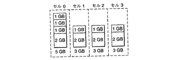
図2は、4個のセル:セル0、セル1、セル2、およびセル3にメモリが分散した分散メモリシステム200を示す。セル0は総計で8ギガバイト(GB)のメモリを含み、セル1は6GBのメモリを含み、セル2は4GBのメモリを含み、セル3は2GBのメモリを含む。一実施形態では、これら4個のセルへのインタリーブは、以下のようにして達成される。まず、インタリーブに利用可能なメモリ量が最小なのはどのセルかについて査定を行う。この場合、セル3は2GBのメモリしか含まない。したがって、インタリーブエントリ0は、セル0、1、2、および3から2GBのメモリ、総計で8GBのメモリをインタリーブする。その結果得られるインタリーブエントリを図3の行305に示す。図3中、各行は最大8個のセルメモリを識別する。行305の上には、3ビットの8つの組み合わせがあり、3ビットの各組み合わせが行305(および行310)における8つのエントリ項目の1つに関連付けられる。3ビットのこれら組み合わせを使用して特定のエントリ項目を識別するが、これについてさらに詳細に後述する。
【0018】
次に、査定を行って、利用可能な任意のセルに残っている最小のメモリ量を決定する。この場合、セル2における2GBである。セル0、セル1、およびセル2にわたるインタリーブは、図4に示す3つのインタリーブエントリを使用することによって提供される。インタリーブエントリ1、2、および3(図4中の3ビット組み合わせの下にある最初の3行それぞれ)は、セル0の二番目の2GBブロック、セル1の二番目の2GBブロック、およびセル2の一番上の2GB部分に使用される。この時点において、インタリーブエントリ0は、総計8GBの情報をアドレス指定するが、インタリーブエントリ1、2、および3はそれぞれ2GBの情報を含む。セル3のメモリリソースは、インタリーブエントリ0で完全に使用されてしまった。セル2のメモリリソースは、インタリーブエントリ3の完成を通して使い尽くされた。
【0019】
本プロセスにおける次のステップは、割り当てられずに残っている任意のセルのメモリを識別することである。この場合、セル1に2GBのメモリが残っている。インタリーブエントリ4は、通常であれば、セル0からの2GBのメモリおよびセル1からの2GBのメモリを含むことになろう。この配列により、すでにマッピングされた14GBに4GBが追加され、総計で18GBになる。しかし、一実施形態では、各テーブルエントリがグループサイズの整数倍で、すなわち16GBで始まることが好ましい。したがって、セル0およびセル1における4GBが1つのインタリーブエントリを占めることができるようにするには、次に2GBを追加する必要がある。このため、インタリーブエントリ4(図示せず)は、セル0にある一番上の2GBを表し、マッピングする。ここで、今までに定義されたインタリーブエントリ(0、1、2、3、および4)は16GBのメモリを含むことになる。インタリーブエントリ5(図示せず)は、セル1にある残りの2GBおよびセル0における残りの2GBをマッピングする。これは、これまでにエントリ0、1、2、3、および4に割り当てられた16GBが4GBの倍数であるため差し支えない。要約すると、セル0〜セル3に含まれる20GBのメモリはここで、6つのインタリーブエントリに含められる。最初のインタリーブエントリは、4個のセルそれぞれから2GBずつ、合わせて8GBの情報を含む。インタリーブエントリ1、2、3、および4は2GBを含み、インタリーブエントリ5は4GBを有する。
【0020】
インタリーブグループは、所与のメモリ範囲でのインタリーブに制限される同量のメモリを有する複数のセルのユニットとして定義される。インタリーブグループは1つまたは複数のインタリーブエントリで構成される。インタリーブグループ0は、インタリーブエントリ0内にある8GB、換言すれば4個のセルそれぞれからの2GBで構成される。インタリーブグループ1は、インタリーブエントリ1、2、および3内にある6GB、換言すればセル0からの2GB、セル1からの2GB、およびセル2からの2GBで構成される。インタリーブグループ2は、セル0の一番上の2GB(すなわち、インタリーブエントリ4)で構成される。インタリーブグループ3は、セル0およびセル1それぞれからの2GBで構成される(すなわち、インタリーブエントリ5)。
【0021】
所望の物理メモリが配置されている特定のセルを識別するには、入力メモリアドレスからの第1のアドレスビットの組を使用してセルマップの行を識別し、入力メモリアドレスからの第2のアドレスビットの組を使用して識別された行にインデックスを付け、エントリ項目を識別する。一実施形態では、44ビットメモリアドレスが使用され、アドレスビット29〜43が第1のアドレスビットの組に対応し、ビット6〜8が第2のアドレスビットの組に対応する。3ビット(たとえば、ビット6〜8)を使用して、8列すなわち8個のエントリ項目を有するエントリにインデックスを付ける。16エントリ項目を有するエントリの場合には、4ビット(たとえば、ビット6〜9)をインデックス付けに使用する。同様に、エントリサイズが倍になるごとに、追加のインデックス付けビットを1個使用する。
【0022】
インタリーブは、アクセスされた連続メモリ量が少なく保たれる場合に最も効果的である。キャッシュラインインタリーブでは、セルマップはキャッシュラインが配置されるセルを示す。このため、インタリーブエントリ0(図3における行305)を再び参照すると、キャッシュラインがセル0、1、2、および3の間でインタリーブされた場合、行305はどのようにセルがテーブル内で表されるかを示す。一実施形態では、行305の上にある複数の3ビット組み合わせでの3ビットは、入力論理メモリアドレスのアドレスビット6〜8に対応する。入力アドレスのこれら3ビットを使用して、行にインデックスを付け、エントリ項目の1つを識別する。行305における各エントリ項目は、4個のセルの1つを識別する。図3に示すように、メモリアドレスのビット6〜8が000である場合、これは、メモリの物理アドレスがセル0にあることをセルコントローラに示す。メモリアドレスのビット6〜8の値が001である場合、これはメモリの物理アドレスがセル1にあることをセルコントローラに示す。同様に、セルコントローラは、メモリアドレスのビット6〜8について可能な他の6つの値それぞれを使用して、テーブルからのセルを識別する。
【0023】
再び図1を参照して、4個のセルを有する単一ノードを示す。各セルはそれぞれのメモリデバイスを有する。しかし、システム全体が2個の4セルノードを有する場合には、それぞれメモリを有する8個のセルが利用可能である。これらセルにセル0〜セル7とラベルを付ける場合、メモリを8個すべてのセルにわたってインタリーブすることができるであろう。図3の行310は、どのようにメモリを8個すべてのセルにインタリーブすることができるかを示す。この場合、3ビット指示子(メモリアドレスのビット6〜8)は、8個のセルのうちいずれがメモリの物理アドレスを含むかを示す。したがって、行310は8ウェイインタリーブを示し、行305は4ウェイインタリーブを示す。
【0024】
システムが3セル構成を有する場合、セルマップは、3ウェイインタリーブを示す図4に示すようになる。3個のセルは、セルマップにおいて3行にわたって効率的にマッピングされる。1行目の1列目は、セル0の値を含む。1行目の2列目は、セル1の値を含む。1行目の3列目は、セル2の値を含む。このシーケンスは、最後のセルが3行目の最後の列で終わるまで繰り返される。
【0025】
セルマップの行は、マスク、コンパレータ、およびメモリアクセスデバイスからのメモリアドレスビットの組み合わせを介してセルコントローラによって識別される。マスクを使用して、適切な行の決定に関係のないアドレスのビットをマスクする。コンパレータは、マスクしたアドレス部分を整合値と比較して、セルマップの対応する行を識別する。
【0026】
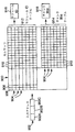
図5は、シングルキャッシュラインインタリーブの場合の64ウェイインタリーブドセルマップエントリを示すブロック図である。図5におけるセルマップエントリは64ウェイインタリーブであるため、メモリアドレスの6ビット(たとえば、ビット6〜11)をエントリへのインデックス付けに使用する。エントリイネーブルブロック510は、入力メモリアドレスのビット29〜ビット43を含むアドレス部分505を使用してセルマップの適切な行を識別する。アドレス範囲は、行選択に使用するアドレス部分505から決定される。図5に示すように、エントリイネーブルブロック510は、以下の式Iを実行する。
【0027】
【数1】
Entry_enable=((ADDR AND MASK)==cmp)式I
【0028】
式Iに示すように、エントリイネーブルブロック510は、アドレス部分505をマスクしてアドレスの最下位ビットを破棄し、マスクされたアドレスをその行の比較値または整合値である「cmp」と比較する。比較における値が等しい場合、Entry_enableに、マッチする行を示す論理的に真の値が割り当てられる。値が等しくない場合、Entry_enableに、マッチしない行であることを示す偽の論理値が割り当てられる。
【0029】
行が選択されると、メモリアドレスのビット6〜11を使用して、セルマップのその行内の64個のエントリ項目の1つを識別し、「CELL」および「Cell_Addr」が決定され、出力される。「CELL」は、セルを一意に識別するセルIDを表し、「Cell_Addr」はセルアドレスを表し、これについてさらに詳細に後述する。図5に示すように、アドレス部分515は、アドレスビット6〜11および29〜42を含み、アドレスビット6〜11および29〜42を使用して適切なセルIDおよびセルアドレスを決定する。アドレス入力520に示すように、さらなる入力によってさらなるテーブルエントリ項目を選択することができる。図5に示すように、以下の式IIに示すような比較を行うことによって列が選択される。
【0030】
【数2】
Column_Select=(ADDR[11:6]==0x0)式II
【0031】
式IIからわかるように、メモリアドレスのビット6〜11を、列に対応する16進数の値(たとえば、この場合では0x0であり、これは一列目に対応する)と比較する。比較している値が等しい場合、Column_Selectは、マッチングを示す真の論理値を含む。比較している値が等しくない場合、Column_Selectは、マッチングがないことを示す偽の論理値を含む。
【0032】
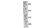
エントリイネーブルブロック510でのコンパレータおよびマスクの使用について、図6を参照してさらに詳細に述べる。図6は、十進数の0〜16を表す二進数を示す。0〜16の範囲の10進数は4つの異なるグループ:0〜3を含むグループ605、4〜7を含むグループ610、8〜11を含むグループ615、および12〜15を含むグループ620に分けられている。マスクを効果的に使用するために、種々のグループを識別する方法が必要である。この場合、最初の2ビット、すなわち最上位2ビット(最左端の2ビット)を使用して各種グループを区別することができることがわかる。グループ605に表示される4つの数はそれぞれ00で始まり、グループ610の中の数はそれぞれ01で始まり、グループ615の中の数はそれぞれ10で始まり、グループ620の中の数はそれぞれ11で始まる。したがって、1100からなるマスクが確立される。重要な各ビットには「1」を配置し、重要ではない、すなわち「無関係な」各ビットには「0」を配置する。コンパレータは、メモリブロックの開始アドレスに等しくセットされる。マスクを使用して、4つのグループ605〜620のいずれに所望のビットシーケンスが存在するかを判定する。2つの最上位ビットの比較により、セルマップ内の特定の行が決定される。
【0033】
コンパレータおよびマスクの使用をさらに説明するため、いくつかの例を考察する。図7を参照すると、ノードは4個のセルを含み、セル0は5GBのメモリを有し、セル1は3GB、セル2も3GB、またセル3も3GBのメモリを有する。16進数表記では、1GBは0X000_40000000である。図7のインタリーブエントリ0は、4個のセルそれぞれから2GB、総計8GBのメモリを含む。このメモリブロックの範囲は0GBから最大8GBである。コンパレータは、0X000_00000000に等しい。マスクの値は、メモリロケーションが8GBよりも大きいかどうかを判定するために調べる必要のあるビットを識別することによって決定される。値が8GBを越えるかどうかを判定するために調べなければならない各ビット位置に、「1」を配置する。このため、16進数表記では、マスクは0Xffe_00000000に等しい。16進数表記での最下位の8つの数で表されるビットは、メモリロケーションの値が8GBを越えているかどうかの判定に必要ないため、調べる必要はない。したがってマスクは、メモリアクセスデバイスの1つからのメモリ値が8GBを越えるか否かを判定するために調べる必要のあるビット位置のみを含む。確立されたこのマスクおよびコンパレータを使用すると、0〜8GBの範囲にあるいずれのアクセスもインタリーブエントリ0しか起動しない。対応するセルマップの適切な行内において、セル番号は0、1、2、3、0、1、2、3として識別され得る。これは、図3における行305と同様である。この構成は、セル0〜3の間での4ウェイインタリーブを達成する。インタリーブエントリ1の場合、ここでも4個すべてのセルが使用されるが、今度は各セルから1GBのメモリのみが使用される。この場合、コンパレータ値は、8GBに等しい0X002_00000000に等しい。これは、このインタリーブエントリの開始値である。この場合のマスク値は、0Xfff_00000000である。インタリーブエントリ1が確立されると、セル0に2GBが残る。
【0034】
概して、インタリーブは、まず最大のブロックにわたって行われるため、続いて次のインタリーブブロックのサイズはより小さい。セル0に残っている2GBは、通常であれば、図7に示す1GBチャンクに分けられる。しかし、この場合、インタリーブエントリ0およびインタリーブエントリ1に含まれる12GBは、セル0に残っている2GBで割り切れる。したがって、インタリーブエントリ2は、セル0に残っている2GBのメモリを含むことになり、コンパレータ値は12GBである0X003_00000000になり、マスク値は0Xfff_80000000になる。
【0035】
最後の例として、図8に示すように、ノードが3個のセルを含み、各セルが2GBのメモリを含む場合、インタリーブは以下のように行われる。インタリーブエントリ0の場合、コンパレータは0X000_00000000、すなわち0GBである。マスクは0Xfff_80000000である。これにより、セル0の最初のGBおよびセル1の最初のGBの間でインタリーブすることができるようになる。この場合の行エントリは、0の後に1が続き、行の全長にわたりこれが交互になったものからなる。これは、ここでもセル0から1GBおよびセル1から1GBというメモリの最初の2GBにわたり2ウェイでインタリーブする。
【0036】
インタリーブエントリ1の場合、コンパレータ値は0X000_80000000であり、これはすなわち2GBに等しい。この場合のマスク値は、0Xfff_80000000である。対応するセルマップ行は、行の全長にわたって1と2が交互になったものであり、これにより、セル1からの2番目のGBおよびセル2からの最初のGBにわたり2ウェイインタリーブすることができる。
【0037】
インタリーブエントリ2は、0X001_00000000のコンパレータ値を有し、これは4GBに等しい。マスク値は、0Xfff_80000000である。このインタリーブエントリのセルマップ内の対応する行は、行の全長にわたって2と0が交互になったものである。このインタリーブエントリは、セル2およびセル0にわたり2ウェイでインタリーブし、最後の2GBのメモリを含む。
【0038】
一実施形態では、セルコントローラは、セルIDだけの場合よりも、より多くの情報をセルマップエントリ項目から取得する。たとえば、セルコントローラをセル0に送る(direct)いくつかのセルマップエントリ項目がありうる。セル0に含まれるメモリは、様々なインタリーブエントリに分けられている場合がある。一実施形態では、セルマップエントリ項目は、セル0のメモリ内のどこに要求される情報が格納されているかの指示もセルコントローラに供給する。本発明の一形態では、CELL_ADDRすなわちセルアドレスを使用して、セルコントローラを特定のメモリアクセスのためにセルメモリ内の特定の512メガバイト(MB)領域に送る。セルアドレス式の一実施形態を以下の式IIIで提供する。
【0039】
【数3】
CELL_ADDR=((ADDR[42:29]&CHUNK_MASK)>>インタリーブ+CHUNK_START式III
【0040】
アドレスビット29〜42は、特定のセル内のどこからデータの読み出しを開始するかを決定する際に使用される。式IIIに含まれるCHUNK_MASKは、先に考察したマスクの逆(inverse:インバース)である。CHUNK_MASKの目的は、セルコントローラをメモリブロックの正確な部分に導くことである。マスクしたアドレス部分は右シフト(記号「>>」で表される)され、インタリーブに使用されていたビットを削除する(式IIIでは「インタリーブ」と表される)。セルマップテーブルが8列を含む場合、3つのインタリーブビットが列の識別に使用される。セルマップが16列を有する場合、列の識別に4ビットが使用される。
【0041】
CHUNK_STARTは、他のインタリーブエントリ専用の、または他のインタリーブエントリによって以前使用されていたメモリの量である。たとえば、再び図2のインタリーブエントリ1を参照すると、インタリーブエントリ1は、インタリーブエントリ0が4個のセルそれぞれから2GBを占めた後に来た。したがって、セル0の2番目の2GB部分がアドレス指定されている場合、CHUNK_STARTはインタリーブエントリ0に含まれた2GBである。あるいは、引き続き図2を参照すると、セル0における2GBおよびセル1における2GBを含むインタリーブエントリ5は、セル0およびセル1の双方における4GBのCHUNK_STARTを有する。要約すると、CELL_ADDR式は、メモリアクセスデバイスからのアドレスビットを使用し、所与のブロック内の特定のメモリロケーションに到達するようにするオフセットに等しいメモリ量を追加し、右シフトしてインタリーブにすでに使用しておりブロック内のロケーションを決定するためにもはや必要のないビットを削除し、他のインタリーブエントリ内のインタリーブにあてられていたセルメモリを追加する。
【0042】
図9は、セルマップ900の一実施形態の図である。セルマップ900は、複数のエントリ904をそれぞれ含むモジュールIDテーブル912およびチャンク開始テーブル914を含む。各エントリ904は複数のエントリ項目910を含む。代替の実施形態では、モジュールID情報およびチャンク開始情報を単一テーブルに組み込むことができる。別の代替実施形態では、セルマップ900はチャンク開始テーブル914を含まない。各エントリ904におけるエントリ項目910中の数は、インタリーブのウェイ数に基づく。たとえば、16ウェイインタリーブの場合、モジュールIDテーブル912およびチャンク開始テーブル914はそれぞれ、エントリ904毎に少なくとも16個のエントリ項目910をそれぞれ含むことになる(図9に示すように)。また、64ウェイインタリーブの場合、モジュールIDテーブル912およびチャンク開始テーブル914はそれぞれ、エントリ904毎に少なくとも64個のエントリ項目910を含むことになる。一実施形態では、モジュールIDテーブル912における各エントリ項目910は、宛先モジュール識別のために8ビットモジュールID値を含み、チャンク開始テーブル914における各エントリ項目910は、メモリロケーションの識別に使用されるチャンク開始値を含む。受信した各入力アドレス902に基づき、後述するように、適切なモジュールID値916およびチャンク開始値918が識別され、セルマップ900から出力される。
【0043】
以下の表1は、セルマップベースシステムの一実施形態を実施する擬似コードを含む。
【0044】
【表1】

上記表1の場合、以下の仮定を行う。すなわち、アドレスサイズの実施は50ビット(すなわち、ビット0〜49)である;各エントリ904は16ウェイインタリーブされる(したがって、エントリ904内でのインデックス付けのために4ビットが必要である);システムはシングルキャッシュラインインタリーブを実行している;キャッシュラインサイズは64バイトである(よって、アドレスビット6〜9がエントリ904内のインデックス付けに使用される);おおよそ32〜64のエントリ904が各プロセッサインタフェースに設けられる;かつ、最小アドレス指定可能メモリは1/2GBである(よって、アドレスマスク(Address Mask)はビット29〜49を使用する)。
【0046】
上記仮定は一例のシステムに基づき、かつ特定の実施に基づいて変更を行いうることが理解されよう。たとえば、キャッシュラインサイズが64バイトではなく128バイトである場合には、入力アドレス902のビット7〜10がエントリ904内のインデックス付けに使用される。キャッシュラインサイズが256バイトである場合は、入力アドレス902のビット8〜11がエントリ904内のインデックス付けに使用される。キャッシュラインサイズが倍になるごとに、4つのインデックス付けビットがそれぞれ左に1ビット位置分シフトする。別の例では、最小アドレス指定可能メモリが1/2GBではなく64メガバイト(MB)である場合、アドレスマスク(Address Mask)は、ビット29〜49ではなくビット24〜49を使用する。種々のキャッシュラインサイズおよび異なる最小アドレス指定可能メモリサイズの他に、種々のアドレスサイズ、シングルキャッシュラインインタリーブではなくマルチキャッシュラインインタリーブ、およびインタリーブの種々のウェイ数を含むがこれらに限定されない他の変更を行うこともできる。
【0047】
表1に列挙される最初の項目はIncoming_Address[49:0]であり、これは入力アドレス902として図9に表される。一実施形態では、入力アドレス902はプロセッサアドレスであり、0〜49の番号が付けられた50ビットを含む。入力アドレス902は、第1のアドレス部分902A、第2のアドレス部分902B、および第3のアドレス部分902Cを含む。
【0048】
表1に列挙される2番目の項目は、Address Match[49:29]である。一実施形態では、セルマップ900における各エントリ904は、Address Match[49:29]の特定の値に関連付けられる。
【0049】
表1に列挙する3番目の項目は、Address Mask[49:29]である。Address Mask[49:29]は、入力アドレス902から関連するビットを抽出するためにセルコントローラ(たとえば、セルコントローラ175)により使用される。一実施形態では、入力アドレス902のビット29〜49は第1のアドレス部分902Aと呼ばれる。セルコントローラ175は、マスクされた第1のアドレス部分902Aを、Address Match値と比較してマッチするエントリ904を識別する。
【0050】
モジュールIDテーブル912におけるエントリ904は、表1に列挙される4番目の項目で表され、この項目はModule_id_table_in_entry[エントリにおけるインタリーブのMax_ways*Bits_per_module_id]である。Module_id_table_in_entryの括弧内の値は、モジュールIDテーブル912におけるエントリ904のビットサイズを表す。各モジュールIDに8ビットを使用し(すなわち、Bits_per_module_id=8)、かつエントリ904が16ウェイインタリーブされる(すなわち、エントリにおけるインタリーブのMax_Ways=16)と仮定すると、モジュールIDテーブル912の各エントリ904に必要なビット数は128(すなわち、8×16)になる。64ウェイインタリーブエントリ904の場合、モジュールIDテーブルエントリ904のサイズは512ビット(すなわち、64×8)になる。モジュールIDにつき8ビットを使用すると、256個のモジュールを一意に識別することができる。特定の実施に応じて、モジュールIDにつき他のビット数を使用してもよい。
【0051】
チャンク開始テーブル914のエントリ904は、表1に列挙される5番目の項目で表され、この項目はChunk_start_table_in_entry[エントリにおけるインタリーブのMax_Ways*0.5GBのチャンクすべてをアドレス指定するために必要なビット数]である。Chunk_start_table_in_entryの括弧内の値は、チャンク開始テーブル914におけるエントリ904のビットサイズを表す。すべての1/2GBチャンクをアドレス指定するために8ビットが使用され、かつエントリ904が16ウェイインタリーブされる(すなわち、エントリにおけるインタリーブのMax_ways=16)と仮定すると、チャンク開始テーブル914の各エントリ904に必要なビット数は128(すなわち、8×16)になる。64ウェイインタリーブエントリ904の場合、チャンク開始テーブルエントリ904のサイズは512ビット(すなわち、64×8)になる。
【0052】
表1に列挙される6番目の項目は、Hit_for_that_entry=((Incoming_Address[49:29]]&Address Mask[49:29])==Address Match[49:29])である。一実施形態では、セルマップ900における各エントリ904は、Address Match[49:29]の特定の値に関連付けられ、表1に列挙される6番目の項目のようなヒット式が、ヒットが識別されるまで、セルマップ900における各エントリ904について実行される。変数Hit_for_that_entryは、(Incoming_Address[49:29]]&Address Mask[49:29])とAddress Match[49:29]の比較に応じて、真の論理値かあるいは偽の論理値のいずれかを含むことになる。(Incoming_Address[49:29]]&Address Mask[49:29])の値とAddress Match[49:29]の値が等しくない場合、Hit_for_that_entryは、偽の論理値になり、マッチしないエントリであることを示す。(Incoming_Address[49:29]]&Address Mask[49:29])の値とAddress Match[49:29]の値が等しい場合、Hit_for_that_entryは、真の論理値になり、マッチするエントリであることを示す。
【0053】
モジュールIDテーブル912の各エントリ904の場合、チャンク開始テーブル914に対応するエントリ904がある。ヒットがエントリ904に対して生成される場合、モジュールIDテーブルエントリからのモジュールID値916が出力され、対応するチャンク開始テーブルエントリからチャンク開始番号918が出力される。一実施形態では、チャンク開始番号918は、モジュールID値916によって識別されるメモリ内のメモリロケーションを識別するための1/2GBの倍数である。エントリ904内の適切なモジュールID値916およびチャンク開始番号918を識別するための式は、表1の7番目および8番目の項目に列挙される。
【0054】
表1に列挙される7番目の項目は、Physical_destination_module=Module_id_table_in_entry[Incoming_Address[9:6]]である。この項目が示すように、入力アドレス902のビット6〜9を使用して、モジュールIDテーブル912でマッチするエントリ904における16個のエントリ項目910の1つを識別する。一実施形態では、入力アドレス902のビット6〜9は第3のアドレス部分902Cと呼ばれる。識別されたエントリ項目910からのモジュールID値は、変数Physical_destination_moduleに格納される。64ウェイインタリーブエントリ904を有するモジュールIDテーブル912の場合、モジュールIDテーブルエントリ904にインデックスを付ける式は、Physical_destination_module=Module_id_table_in_entry[Incoming_Address[11:6]]である。この場合、第3のアドレス部分902Cはアドレスビット6〜11を含み、これらのアドレスビットを使用してモジュールIDテーブルエントリ904にインデックスを付ける。
【0055】
表1に列挙される8番目の項目は、Chunk_start=Chunk_start_table_in_entry[Incoming_Address[9:6]]である。この項目が示すように、入力アドレス902の第3のアドレス部分902Cを使用して、チャンク開始テーブル914でマッチするエントリ904における16個のエントリ項目910の1つを識別する。識別されたエントリ項目910からのチャンク開始番号が変数chunk_startに格納される。64ウェイインタリーブエントリ904を有するチャンク開始テーブル914の場合には、チャンク開始テーブルエントリ904にインデックスを付けるための式は、Chunk_start=Chunk_start_table_in_entry[Incoming_Address[11:6]]である。この場合、第3のアドレス部分902Cはアドレスビット6〜11を含み、これらのアドレスビットをチャンク開始テーブルエントリ904へのインデックス付けに使用する。上述したように、一実施形態では、特定のメモリロケーションを識別するために、チャンク開始値をセルアドレス式(たとえば、式III)で使用する。
【0056】
セルマップ900等のセルマップを使用してI/O仮想化を達成するため、メモリに使用されるエントリ904とI/Oに使用されるエントリ904とを区別する機構が設けられる。また、I/Oタイプエントリ904の場合、モジュールIDテーブル912へのインデックス付けに使用する種々のアドレスビットの組の選択に複数のオプションを提供することができる。したがって、メモリタイプエントリとI/Oタイプエントリとを区別するために、かつI/Oに追加のインデックスオプションを提供するために、追加の状態がセルマップ900に設けられる。一実施形態では、セルマップ900がチャンク開始テーブル914を含む場合、メモリタイプエントリ904のみが関連するエントリをチャンク開始テーブル914に含み、チャンク番号はI/Oタイプエントリ904で使用されない。
【0057】
一実施形態では、セルマップ900におけるエントリ904は、1ビットのエントリタイプ識別子906を含む。本発明の一形態では、エントリタイプ識別子906の値が0である場合、エントリ904はメモリタイプエントリであり、エントリタイプ識別子906の値が1の場合、エントリ904はI/Oタイプエントリである。また、一実施形態では、エントリ904は2ビットのインデックス選択識別子908を含む。インデックス選択識別子908の2ビットは、可能な4つの異なる値を提供し、これらの値を使用して、I/Oテーブルエントリ904についてモジュールIDテーブル912にインデックスを付けるためのアドレスビットの組を選択する。
【0058】
セルマップ900におけるメモリタイプエントリ904の場合、ヒットロジック、モジュールID識別、およびチャンク開始番号識別は、上述したものと同じである。具体的には、表1の6番目の項目に示すように、Hit_for_that_entry=((Incoming_Address[49:29]]&Address Mask[49:29])==Address Match[49:29])である。よって、入力アドレス902のビット29〜49(すなわち、第1のアドレス部分902A)を使用して、セルマップ900におけるマッチするエントリ904を識別する。また、表1の7番目および8番目の項目に示すように、入力アドレス902のビット6〜9(すなわち、第3のアドレス部分902C)を使用して、モジュールIDテーブル912におけるメモリタイプエントリ904およびチャンク開始テーブル914におけるチャンク開始エントリ904にインデックスを付ける。
【0059】
一実施形態では、I/Oタイプエントリ904の場合、ヒットロジックはメモリタイプエントリ904の場合に使用したものと同じであるが、より少ない数のアドレスビットが比較される。本発明の一形態では、これは、Address MatchレジスタおよびAddress Maskレジスタにおいてより多くのビットをマスクすることによって達成される。また、I/Oタイプエントリ904の場合、モジュールIDテーブル912へのインデックスは、メモリタイプエントリ904の場合とは別様に選択される。第2のアドレス部分902Bと呼ぶ、I/Oタイプエントリ904にインデックスを付けるために使用される入力アドレスビットの組は、そのエントリ904のインデックス選択識別子908に基づいて選択される。以下の表2は、本発明の一実施形態によるインデックス選択識別子908の値およびインデックス付けに使用される対応する入力アドレスビットを示す。
【0060】
【表2】
ヒットが決定された(すなわち、セルマップ900におけるエントリ904が第1のアドレス部分902に基づいて識別された)後、識別されたエントリ904内の特定のエントリ項目910がインデックス値に基づいて選択される。以下の表3は、本発明の一実施形態によるモジュールIDテーブル912におけるエントリ904にインデックスを付けるための擬似コードを含む。
【0062】
【表3】
最初の「switch」コードセグメントは、マッチするエントリ904についてインデックス選択識別子908の値に基づいてindex_module_table_ioに値を割り当てる。次に、入力アドレスのビット6〜9(すなわち、第3のアドレス部分902C)に基づいてindex_module_table_memに値を割り当てる。2番目の「switch」コードセグメントは、マッチするエントリ904のエントリタイプ906に基づいてindex_module_tableに値を割り当てる。エントリ904がメモリ(MEM)タイプエントリである場合、index_module_tableにはindex_module_table_memの値が割り当てられる。エントリがI/Oタイプエントリである場合、index_module_tableにはindex_module_table_ioの値が割り当てられる。最後に、index_module_tableに割り当てられた値を、マッチするエントリ904(すなわち、Module_id_table_in_entry)のインデックスとして使用して、エントリ904における16個のエントリ項目910の1つを識別する。識別されたエントリ項目904は、変数「Physical Destination Module」に割り当てられるモジュールを識別するための識別情報を含む。メモリタイプエントリ904の場合、対応するエントリ904からのチャンク開始値およびチャンク開始テーブル914におけるエントリ項目910もまた上述のように識別される。
【0064】
よって、セルマップエントリ904のタイプに応じて、適切なモジュール情報が抽出および使用される。代替の実施形態では、複数のエントリ904を連結して、より多数のモジュールを仮想化することができる。
【0065】
本発明の一実施形態は、セルマップ900を使用してI/Oモジュール170の仮想化およびメモリインタリーブを提供する。本発明の一形態では、I/Oモジュール170は、周辺コンポーネント相互接続(PCI)デバイス等の複数のI/Oカードまたはデバイスを制御するようにそれぞれ構成されたI/Oコントローラである。したがって、入力アドレス902が第1のI/Oモジュールに向けられ、かつセルマップ900を使用してアクセスを第2のI/Oモジュールにリダイレクトされる場合、第2のI/Oモジュール下のI/Oデバイスは、ソフトウェアからは第1のI/Oモジュール下のI/Oデバイスと同じように見えるはずである。代替の実施形態では、仮想化をI/Oカードまたはデバイスのレベルにまで拡張することができる。
【0066】
本発明の一形態は、同じセルマップインフラストラクチャをメモリインタリーブおよびI/O仮想化の双方に使用することにより、メモリインタリーブ化およびI/O仮想化に別個の構造を設計する必要性をなくす。本発明の一実施形態では、仮想化することのできるモジュールの数に制限がない。本発明の一形態は、ソフトウェア介入なしで、または最小限のサポートでI/Oモジュール170を変更可能なシステムを構築できるようにする。一実施形態では、本発明は、I/Oの仮想化において、従来提供されているシステムよりも高い柔軟性を提供する。また、本発明の一形態では、単一のセルマップエントリ904を使用して複数のI/Oモジュール170を仮想化することができ、またセルマップエントリ904をメモリ目的とI/O目的とで交換して使用することができる。この発明は、例として次のような実施形態を含む。
【0067】
(1) 連続した論理アドレス空間を使用して、複数のメモリ(130、135、140、145)にインタリーブ方式でアクセスし、複数の入出力モジュール(170)にアクセスする方法であって、
複数のエントリ(904)を含む少なくとも1つのマップテーブル(900)を設けることであって、前記エントリ(904)はそれぞれエントリタイプ識別子(906)および複数のエントリ項目(910)を含み、前記エントリ項目(910)はそれぞれモジュール識別子を含み、前記エントリ(904)はそれぞれメモリタイプエントリおよび入出力タイプエントリの一方であり、
複数のアドレスビット(902A〜902C)を含む第1の論理アドレス(902)を受信することと、
前記アドレスビットの第1の組に基づいて、前記少なくとも1つのマップテーブルにおけるエントリを識別することと、
前記識別されたエントリの前記エントリタイプ識別子に基づいて、前記識別されたエントリのタイプを決定することと、
前記エントリタイプ識別子が入出力タイプエントリを示す場合、前記アドレスビットの第2の組に基づいて前記識別されたエントリにおけるエントリ項目を識別することと、
前記エントリタイプ識別子がメモリタイプエントリを示す場合、前記アドレスビットの第3の組に基づいて前記識別されたエントリにおけるエントリ項目を識別することと、
前記識別されたエントリ項目の前記モジュール識別子によって識別されたモジュールにアクセスすることと
を含む方法。
【0068】
(2) 前記少なくとも1つのマップテーブルにおける各入出力タイプエントリは、インデックス選択識別子(908)をさらに含み、
前記識別されたエントリの前記インデックス選択識別子に基づいて、前記第2のアドレスビットの組に使用するアドレスビットを識別することをさらに含む(1)記載の方法。
【0069】
(3) 前記インデックス選択識別子はそれぞれ、複数のインデックス値の1つであり、前記インデックス値はそれぞれアドレスブロックサイズに対応する(2)記載の方法。
【0070】
(4) 前記第1のアドレスビットの組は、前記第2のアドレスビットの組よりも上位のビットを含み、前記第2のアドレスビットの組は、前記第3のアドレスビットの組よりも上位のビットを含む(1)記載の方法。
【0071】
(5) 前記少なくとも1つのマップテーブルに複数のメモリオフセット値(914)を格納することと、
前記第1の論理アドレスに基づいて前記メモリオフセット値(914)の1つを識別することとをさらに含み、
前記エントリタイプ識別子がメモリタイプエントリを示す場合、前記識別されたエントリ項目の前記モジュール識別子によって識別される前記モジュールは、前記識別されたメモリオフセット値に少なくとも部分的に基づいてメモリロケーションにおいてアクセスされる(1)記載の方法。
【0072】
(6) マルチビットマスク値を設けることと、
複数のマルチビット整合値を設けることと、
前記マルチビットマスク値を使用して前記第1の論理アドレスから前記第1のアドレスビットの組を抽出することと、
該抽出された第1のアドレスビットの組を前記複数のマルチビット整合値と比較してマッチングを識別することと
をさらに含む(1)記載の方法。
【0073】
(7) 前記メモリはそれぞれ少なくとも1つのメモリセグメントを含み、前記メモリセグメントはグループに編成され、各グループの前記メモリセグメントは均等なサイズを有し、また前記少なくとも1つのマップテーブルにおける各メモリタイプエントリは、前記メモリセグメントグループの1つに対応する(1)記載の方法。
【0074】
(8) 連続した論理アドレス空間を複数のモジュールにマッピングする方法であって、前記複数のモジュールはメモリ(130、135、140、145)および入出力モジュール(170)を含み、前記論理アドレス空間における各論理アドレス(902)は第1、第2、および第3のアドレス部分(902A〜902C)を含み、
複数のエントリ(904)を含むマップテーブル(900)を設けることであって、前記エントリ(904)はそれぞれエントリタイプ識別子(906)および複数のエントリ項目(910)を含み、前記エントリ(904)はそれぞれメモリタイプエントリおよび入出力タイプエントリの一方であり、前記各エントリ項目(910)は前記複数のモジュールの1つを識別するモジュール識別子を含み、
論理アドレスの組を前記エントリのそれぞれに関連付けることであって、個々のエントリそれぞれに関連付けられる前記論理アドレスの組は、前記第1のアドレス部分について共通する値を含み、前記第1のアドレス部分についての前記共通の値は前記エントリそれぞれごとに異なり、
前記エントリに関連する前記論理アドレスの組の前記第2および前記第3のアドレス部分に基づいて各エントリ内のエントリ項目にインデックスを付けることであって、インデックス付けに使用される前記アドレス部分の選択は、前記エントリの前記エントリタイプ識別子に基づく、
を含む方法。
【0075】
(9) 連続した論理アドレス空間を使用して複数のモジュールへのアクセスを提供するシステム(100)であって、前記モジュールはメモリ(130、135、140、145)および入出力モジュール(170)を含み、
複数のエントリ(904)を含む少なくとも1つのマップテーブル(900)であって、前記エントリ(904)はそれぞれエントリタイプ識別子(906)および複数のエントリ項目(910)を含み、前記エントリ(904)はそれぞれメモリタイプエントリおよび入出力タイプエントリの一方であり、前記エントリ項目(910)はそれぞれ複数のモジュールの1つを識別する、少なくとも1つのマップテーブル(900)と、
論理アドレスを受信するコントローラ(175)であって、受信した論理アドレス(902)の第1の部分に基づいて前記少なくとも1つのマップテーブルにおけるエントリを識別し、該識別されたエントリの前記エントリタイプ識別子および前記受信した論理アドレスの第2の部分に基づいて前記識別されたエントリにおけるエントリ項目を選択し、該選択されたエントリ項目によって識別されるモジュールに基づいてモジュール識別情報を出力するように構成されるコントローラ(175)とを備えるシステム。
【0076】
(10) 前記第2の部分のロケーションは、前記識別されたエントリのタイプに基づいて、前記受信した論理アドレス内で変化する(9)記載のシステム。
【0077】
好ましい実施形態の説明を目的として、本発明の特定の実施形態を本明細書に図示し説明したが、本発明の範囲から逸脱することなく図示し説明した特定の実施形態を多種多様な代替および/または同等の実施で置き換えてもよいことが当業者には理解されよう。化学、機械、電気機械、電気、およびコンピュータの分野における当業者は、本発明が非常に広範囲の実施形態において実施されうることをたやすく理解しよう。本願は、本明細書に述べた好ましい実施形態のあらゆる改変または変形を網羅するものである。したがって、本発明は特許請求の範囲およびその等価物によってのみ制限されるものと明らかに意図される。
【図面の簡単な説明】
【図1】4個のセルおよび1個のクロスバーを含むノードを示すブロック図である。
【図2】メモリが4個のセルに分散する分散メモリシステムを示すブロック図である。
【図3】4ウェイインタリーブおよび8ウェイインタリーブを示すテーブルである。
【図4】3ウェイインタリーブを示すテーブルである。
【図5】シングルキャッシュラインインタリーブの64ウェイインタリーブドセルマップエントリを示すブロック図である。
【図6】インタリーブグループの間での顕著な特徴を識別するチャートである。
【図7】2のべき乗ではないメモリ量を含むセルにわたるインタリーブのブロック図である。
【図8】3個のセルにわたるインタリーブのブロック図である。
【図9】本発明の一実施形態によるメモリインタリーブおよびI/O仮想化を提供するセルマップの図である。[0001]
[Technical field to which the invention pertains]
The present invention relates generally to cell maps for computer systems, and more particularly to a system and method for using a cell map to virtualize input/output modules and interleave memory.
[0002]
2. Description of the Related Art
This application is related to U.S. Patent Application No. 2000/0133664, filed April 29, 2000, entitled "MEMORY ADDRESS INTERLEAVING AND OFFSET BITS FOR CELL INTERLEAVING OF MEMORY."
[0003]
Historically, main memory has been physically located on a central bus. In this type of system, a memory request consisting of a complete physical address is forwarded to the memory subsystem and the data is returned. In a distributed memory system, main memory is physically distributed across many different cells. A cell may consist of several processors, input/output (I/O) devices, cell controllers, and memory.
[0004]
In a distributed system, memory may or may not be interleaved. Prior art memory interleaving systems and methods are described and illustrated, for example, in U.S. Patent No. 5,399,313, issued to Williams et al. on June 25, 1996, entitled "METHODS AND APPARATUS FOR INTERLEAVING MEMORY TRANSACTIONS INTO AN ARBITRARY NUMBER OF BANKS," and U.S. Patent No. 5,399,313, issued to Brockmann et al. on March 8, 1994, entitled "FLEXIBLE N-WAY MEMORY INTERLEAVING," both of which are assigned to the owner of the present invention. In a non-interleaved access method, where memory is divided into or across multiple physical cells, the contiguous memory space is addressed as a cohesive block by first sequentially accessing all memory in the first cell, then sequentially accessing all available memory in the second cell, and so on. If each cell were configured with the maximum amount of memory possible, the memory would appear to the system as one contiguous block of memory and would be addressed as one contiguous block of memory. However, if not all cells are configured with maximum memory capacity, this non-interleaving scheme may result in holes in the memory space corresponding to lost memory blocks in the cells. Non-interleaved memory also tends to use both instructions and data sequentially, necessitating multiple sequential accesses to a particular cell. A processor that continuously or frequently accesses remote memory in another cell, while benefiting from local storage, consumes significant overhead, including processing and communication resources in both the local and remote cells, as well as the connecting network. Over time, these resources may become unavailable for other processes, causing degradation of system performance.
[0005]
Alternatively, memory in a distributed memory system can be accessed via an interleaving protocol. Interleaving memory across several cells allows for more even access to memory. For example, if a system includes two cells connected together via a bus system, with each cell including a memory and four separate processors, interleaving memory in
[0006]
As an example of interleaving, assume that the memory contained in a system is distributed among four cells labeled 0, 1, 2, and 3. Assume further that
[0007]
Large computer systems use cell maps to distribute processor accesses to avoid hot spots. Cell maps are used to find destination modules for cell/node based systems. Cell maps are used to interleave memory into cells to provide a more even access pattern to the memory. Cell map entries have been used to provide 1, 2, 4, 8, 16, 32, and 64 way interleaving. The size of the cell map entry determines the number of ways the memory is interleaved.
[0008]
Some of the conventional systems mentioned above use cell maps to implement virtualization and memory interleaving. The memory interleaving is generally fine-grained, with two addresses to adjacent cache lines going to different modules. Such fine-grained access is typically not needed for input/output (I/O) virtualization.
[0009]
In conventional systems, separate resources are used for memory mapping and I/O mapping. Depending on the system's topology and architecture, and depending on the system's current needs, the system "flips-flops" to provide the desired memory or I/O operations. Also, the programming models for interleaved memory and mapping I/O modules are quite different.
[0010]
[Patent Document 1]
U.S. Patent Application No. 09/563,018
U.S. Patent No. 5,530,837
U.S. Patent No. 5,293,607
[Problem to be solved by the invention]
It would be desirable to provide memory interleaving and I/O module virtualization using a single cell map structure.
[0012]
[Means for solving the problem]
One aspect of the present invention provides a method for accessing interleaved memories and I/O modules using a contiguous logical address space. At least one map table is provided. The at least one map table includes a plurality of entries. Each entry includes an entry type identifier and a plurality of entry items. Each entry item includes a module identifier. Each entry is one of a memory type entry and an I/O type entry. A first logical address is received. The first logical address includes a plurality of address bits. An entry in the at least one map table is identified based on a first set of address bits. A type of the identified entry is determined based on an entry type identifier of the identified entry. If the entry type identifier indicates an I/O type entry, an entry item of the identified entry is identified based on a second set of address bits. If the entry type identifier indicates a memory type entry, an entry item of the identified entry is identified based on a third set of address bits. A module identified by the module identifier of the identified entry item is accessed.
[0013]
[0023]
In the following detailed description of the preferred embodiment, reference is made to the accompanying drawings which form a part hereof, and which show, by way of illustration, specific embodiments in which the invention may be practiced. It is to be understood that other embodiments may be utilized and structural or logical changes may be made without departing from the scope of the present invention. Therefore, the following detailed description is not to be taken in a limiting sense, and the scope of the present invention is defined by the appended claims.
[0014]
1 is a block diagram illustrating a processing system or
[0015]
Each of the four processors 150-165 and the I/
[0016]
One embodiment of a cell map is a table having multiple rows and multiple columns, where each row corresponds to an interleave entry and each column in a row corresponds to an entry item that identifies one of the cells in the system.
[0017]
FIG. 2 illustrates a distributed
[0018]
An assessment is then made to determine the minimum amount of memory remaining in any available cell, in this
[0019]
The next step in the process is to identify any cell memory remaining unallocated. In this case, there is 2 GB of memory remaining in
[0020]
An interleave group is defined as a unit of cells with the same amount of memory that is restricted to interleaving in a given memory range. An interleave group is composed of one or more interleave entries.
[0021]
To identify the particular cell in which the desired physical memory is located, a first set of address bits from the input memory address is used to identify a row of the cell map, and a second set of address bits from the input memory address is used to index the identified row and identify an entry item. In one embodiment, a 44-bit memory address is used, with address bits 29-43 corresponding to the first set of address bits and bits 6-8 corresponding to the second set of address bits. Three bits (e.g., bits 6-8) are used to index an entry with eight columns or eight entry items. For an entry with 16 entry items, four bits (e.g., bits 6-9) are used for indexing. Similarly, an additional indexing bit is used for each doubling of the entry size.
[0022]
Interleaving is most effective when the amount of contiguous memory accessed is kept small. In cache line interleaving, the cell map indicates the cells in which the cache lines are located. Thus, referring back to interleave entry 0 (
[0023]
Referring again to FIG. 1, a single node is shown with four cells. Each cell has its own memory device. However, if the entire system has two four-cell nodes, then eight cells, each with a memory, are available. If we label the
[0024]
If the system has a three-cell configuration, the cell map will look as shown in Figure 4, which illustrates a three-way interleave. The three cells are effectively mapped across three rows in the cell map. The first column of
[0025]
A row of the cell map is identified by the cell controller through a combination of a mask, a comparator, and memory address bits from the memory access device. The mask is used to mask bits of the address that are not relevant to determining the appropriate row. The comparator compares the masked address portion with a match value to identify the corresponding row of the cell map.
[0026]
Figure 5 is a block diagram illustrating a 64-way interleaved cell map entry for single cache line interleaving. Because the cell map entries in Figure 5 are 64-way interleaved, six bits of the memory address (e.g., bits 6-11) are used to index into the entry. An entry enable
[0027]
##EQU00011##
Entry_enable=((ADDR AND MASK)==cmp)Formula I
[0028]
As shown in equation I, entry enable
[0029]
Once a row is selected, bits 6-11 of the memory address are used to identify one of 64 entry items within that row of the cell map, and "CELL" and "Cell_Addr" are determined and output. "CELL" represents a cell ID that uniquely identifies a cell, and "Cell_Addr" represents a cell address, which will be described in more detail below. As shown in FIG. 5,
[0030]
##EQU00022##
Column_Select=(ADDR[11:6]==0x0) Formula II
[0031]
As can be seen from Equation II, bits 6-11 of the memory address are compared to the hexadecimal value corresponding to the column (e.g., 0x0 in this case, which corresponds to the first column). If the compared values are equal, Column_Select contains a true logical value indicating a match. If the compared values are not equal, Column_Select contains a false logical value indicating no match.
[0032]
The use of comparators and masks in entry enable
[0033]
To further illustrate the use of the comparator and mask, consider some examples. With reference to FIG. 7, a node contains four cells, with
[0034]
Typically, interleaving occurs over the largest blocks first, so that the next interleaved block is smaller in size. The 2 GB remaining in
[0035]
As a final example, as shown in Figure 8, if a node contains 3 cells, each containing 2 GB of memory, interleaving would be done as follows: For
[0036]
For
[0037]
[0038]
In one embodiment, the cell controller obtains more information from the cell map entry item than just the cell ID. For example, there may be several cell map entry items that direct the cell controller to
[0039]
##EQU00033##
CELL_ADDR=((ADDR[42:29] &CHUNK_MASK)>>INTERLEAVE+CHUNK_START Equation III
[0040]
Address bits 29-42 are used in determining where to start reading data within a particular cell. CHUNK_MASK, contained in Equation III, is the inverse of the mask discussed above. The purpose of CHUNK_MASK is to direct the cell controller to the correct portion of the memory block. The masked address portion is right shifted (represented by the symbol >>) to remove the bits used for interleaving (represented as "interleave" in Equation III). If the cell map table contains 8 columns, then 3 interleave bits are used to identify the columns. If the cell map has 16 columns, then 4 bits are used to identify the columns.
[0041]
CHUNK_START is the amount of memory dedicated to or previously used by other interleave entries. For example, referring again to interleave
[0042]
FIG. 9 is a diagram of one embodiment of a
[0043]
Table 1 below contains pseudocode for implementing one embodiment of a cell map based system.
[0044]
Table 1
For Table 1 above, the following assumptions are made: the implementation address size is 50 bits (i.e., bits 0-49); each
[0046]
It will be appreciated that the above assumptions are based on an example system and may be modified based on the particular implementation. For example, if the cache line size is 128 bytes instead of 64 bytes, then bits 7-10 of the
[0047]
The first item listed in Table 1 is Incoming_Address[49:0], which is represented in Figure 9 as
[0048]
The second item listed in Table 1 is Address Match[49:29]. In one embodiment, each
[0049]
The third item listed in Table 1 is Address Mask[49:29]. Address Mask[49:29] is used by a cell controller (e.g., cell controller 175) to extract relevant bits from
[0050]
An
[0051]
An
[0052]
The sixth item listed in Table 1 is Hit_for_that_entry=((Incoming_Address[49:29]] & Address Mask[49:29]) == Address Match[49:29]). In one embodiment, each
[0053]
For each
[0054]
The seventh item listed in Table 1 is Physical_destination_module=Module_id_table_in_entry[Incoming_Address[9:6]]. As this item indicates, bits 6-9 of the
[0055]
The eighth entry listed in Table 1 is Chunk_start=Chunk_start_table_in_entry[Incoming_Address[9:6]]. As this entry indicates, the
[0056]
To achieve I/O virtualization using a cell map such as
[0057]
In one embodiment, the
[0058]
For a
[0059]
In one embodiment, for I/
[0060]
Table 2
After a hit is determined (i.e., an
[0062]
Table 3
The first "switch" code segment assigns a value to index_module_table_io based on the value of the
[0064]
Thus, the appropriate module information is extracted and used depending on the type of
[0065]
One embodiment of the present invention uses
[0066]
One aspect of the present invention uses the same cell map infrastructure for both memory interleaving and I/O virtualization, eliminating the need to design separate structures for memory interleaving and I/O virtualization. In one embodiment of the present invention, there is no limit to the number of modules that can be virtualized. One aspect of the present invention allows for the creation of a system in which I/
[0067]
(1) A method for accessing a plurality of memories (130, 135, 140, 145) in an interleaved manner and for accessing a plurality of input/output modules (170) using a continuous logical address space, comprising:
providing at least one map table (900) including a plurality of entries (904), each of said entries (904) including an entry type identifier (906) and a plurality of entry items (910), each of said entry items (910) including a module identifier, each of said entries (904) being one of a memory type entry and an I/O type entry;
Receiving a first logical address (902) including a plurality of address bits (902A-902C);
identifying an entry in the at least one map table based on the first set of address bits;
determining a type of the identified entry based on the entry type identifier of the identified entry;
if the entry type identifier indicates an I/O type entry, identifying an entry item in the identified entry based on a second set of address bits;
if the entry type identifier indicates a memory type entry, identifying an entry item in the identified entry based on a third set of address bits;
and accessing a module identified by the module identifier of the identified entry item.
[0068]
(2) each I/O type entry in the at least one map table further includes an index selection identifier (908);
2. The method of
[0069]
(3) The method of (2), wherein each of the index selection identifiers is one of a plurality of index values, each of the index values corresponding to an address block size.
[0070]
(4) The method of (1), wherein the first set of address bits includes more significant bits than the second set of address bits, and the second set of address bits includes more significant bits than the third set of address bits.
[0071]
(5) storing a plurality of memory offset values (914) in the at least one map table; and
and identifying one of the memory offset values (914) based on the first logical address;
2. The method of
[0072]
(6) providing a multi-bit mask value;
providing a plurality of multi-bit match values;
extracting the first set of address bits from the first logical address using the multi-bit mask value;
2. The method of
[0073]
(7) The method of (1), wherein each of the memories includes at least one memory segment, the memory segments being organized into groups, the memory segments of each group having equal sizes, and each memory type entry in the at least one map table corresponds to one of the memory segment groups.
[0074]
(8) A method of mapping a contiguous logical address space onto a plurality of modules, the plurality of modules including a memory (130, 135, 140, 145) and an input/output module (170), each logical address (902) in the logical address space including first, second, and third address portions (902A-902C);
providing a map table (900) including a plurality of entries (904), each of the entries (904) including an entry type identifier (906) and a plurality of entry items (910), each of the entries (904) being one of a memory type entry and an I/O type entry, each of the entry items (910) including a module identifier that identifies one of the plurality of modules;
associating a set of logical addresses with each of the entries, the set of logical addresses associated with each respective entry including a common value for the first address portion, the common value for the first address portion being different for each of the entries;
indexing entry items within each entry based on the second and third address portions of the set of logical addresses associated with the entry, wherein selection of the address portions used for indexing is based on the entry type identifier of the entry;
The method includes:
[0075]
(9) A system (100) for providing access to a plurality of modules using a contiguous logical address space, the modules including a memory (130, 135, 140, 145) and an input/output module (170);
at least one map table (900) including a plurality of entries (904), each of the entries (904) including an entry type identifier (906) and a plurality of entry items (910), each of the entries (904) being one of a memory type entry and an I/O type entry, each of the entry items (910) identifying one of a plurality of modules;
a controller (175) configured to receive a logical address, identify an entry in the at least one map table based on a first portion of the received logical address (902), select an entry item in the identified entry based on the entry type identifier of the identified entry and a second portion of the received logical address, and output module identification information based on a module identified by the selected entry item.
[0076]
10. The system of claim 9, wherein the location of the second portion varies within the received logical address based on the type of the identified entry.
[0077]
Although specific embodiments of the invention have been shown and described herein for purposes of illustrating the preferred embodiments, those skilled in the art will appreciate that a wide variety of alternative and/or equivalent implementations may be substituted for the specific embodiments shown and described without departing from the scope of the invention. Those skilled in the chemical, mechanical, electromechanical, electrical, and computer arts will readily appreciate that the invention may be implemented in a very wide variety of embodiments. This application is intended to cover any and all modifications or variations of the preferred embodiments described herein. It is manifestly intended, therefore, that the invention be limited only by the claims and the equivalents thereof.
[Brief description of the drawings]
FIG. 1 is a block diagram showing a node including four cells and a crossbar.
FIG. 2 is a block diagram showing a distributed memory system in which memory is distributed across four cells.
FIG. 3 is a table showing 4-way interleaving and 8-way interleaving.
FIG. 4 is a table showing three-way interleaving.
FIG. 5 is a block diagram illustrating a 64-way interleaved cell map entry with single cache line interleave.
FIG. 6 is a chart identifying salient features among interleave groups.
FIG. 7 is a block diagram of interleaving across cells containing memory amounts that are not powers of two.
FIG. 8 is a block diagram of interleaving across three cells.
FIG. 9 is a diagram of a cell map providing memory interleaving and I/O virtualization according to one embodiment of the present invention.
Claims (3)
前記複数のモジュールを複数のインタリーブエントリに分け、該複数のインタリーブエントリに対応する複数のエントリを含む少なくとも1つのマップテーブルを設けることであって、前記複数のエントリのそれぞれは、メモリタイプエントリか入出力タイプエントリかを示すエントリタイプ識別子を含むと共に、該インタリーブエントリに含まれるモジュールのうちの1つを特定するためのモジュール識別子を含むエントリ項目を複数含み、さらに、前記入出力タイプエントリのそれぞれは、インデックス選択識別子を含んでおり、該インデックス選択識別子は、予め決められた複数の値のうちの1つを取り、該複数の値は、異なるアドレスサイズに対応づけられている、ことと、
複数のアドレスビットからなる論理アドレスを受信することと、
前記複数のアドレスビットのうちの第1アドレス部分に基づいて、前記少なくとも1つのマップテーブルにおけるエントリを識別することと、
前記識別されたエントリの前記エントリタイプ識別子に基づいて、前記識別されたエントリのタイプを決定することと、
前記エントリタイプ識別子が入出力タイプエントリを示す場合、前記複数のアドレスビットのうちの第2アドレス部分に基づいて、前記識別されたエントリにおけるエントリ項目を識別することであって、該第2アドレス部分に使用するアドレスビットは、前記識別されたエントリの前記インデックス選択識別子の値に基づいて、前記論理アドレスの前記複数のアドレスビットから特定される、ことと、
前記エントリタイプ識別子がメモリタイプエントリを示す場合、前記複数のアドレスビットのうちの第3アドレス部分に基づいて、前記識別されたエントリにおけるエントリ項目を識別することと、
前記識別されたエントリ項目の前記モジュール識別子によって識別されたモジュールにアクセスすることと、
を含む方法。 1. A method for accessing a plurality of modules using a contiguous logical address space, the plurality of modules including a plurality of memories and a plurality of input/output modules;
dividing the plurality of modules into a plurality of interleave entries, and providing at least one map table including a plurality of entries corresponding to the plurality of interleave entries , each of the plurality of entries including an entry type identifier indicating whether the entry is a memory type entry or an I/O type entry, and including a plurality of entry items including a module identifier for identifying one of the modules included in the interleave entry, each of the I/O type entries including an index selection identifier, the index selection identifier taking one of a plurality of predetermined values, the plurality of values corresponding to different address sizes;
receiving a logical address comprising a plurality of address bits;
identifying an entry in the at least one map table based on a first address portion of the plurality of address bits;
determining a type of the identified entry based on the entry type identifier of the identified entry;
if the entry type identifier indicates an I/O type entry, identifying an entry item in the identified entry based on a second address portion of the plurality of address bits , where address bits to be used for the second address portion are determined from the plurality of address bits of the logical address based on a value of the index selection identifier of the identified entry;
if the entry type identifier indicates a memory type entry, identifying an entry item in the identified entry based on a third address portion of the plurality of address bits;
accessing a module identified by the module identifier of the identified entry item;
The method includes:
前記複数のモジュールを複数のインタリーブエントリに分け、該複数のインタリーブエントリに対応する複数のエントリを含むマップテーブルを設けることであって、前記複数のエントリのそれぞれは、メモリタイプエントリか入出力タイプエントリかを示すエントリタイプ識別子を含むと共に、該インタリーブエントリに含まれるモジュールのうちの1つを特定するためのモジュール識別子を含むエントリ項目を複数含み、前記入出力タイプエントリは、さらに、インデックス選択識別子を含んでおり、該インデックス選択識別子は、予め決められた複数の値のうちの1つを取り、該複数の値は、異なるアドレスサイズに対応づけられている、ことと、
一組の前記論理アドレスを、対応する前記エントリに関連付けることであって、或るエントリに関連づけられる該一組の論理アドレスは、前記第1のアドレス部分において共通する値を含み、前記第1のアドレス部分についての前記共通の値は、エントリ間で異なっている、ことと、
前記関連づけられたエントリの前記エントリタイプ識別子が前記入出力タイプエントリを示す場合、前記一組の論理アドレスの前記第2のアドレス部分に基づいて、該エントリの各エントリ項目を特定することであって、該第2のアドレス部分に使用されるアドレスビットは、該エントリの前記インデックス選択識別子の値に基づいて、該論理アドレスを構成するアドレスビットから特定され、
前記関連づけられたエントリの前記エントリタイプ識別子が前記メモリタイプエントリを示す場合、前記一組の論理アドレスの前記第3のアドレス部分に基づいて、該エントリの各エントリ項目を特定することと、
を含む方法。 1. A method of mapping a contiguous logical address space onto a plurality of modules, the plurality of modules including a plurality of memories and a plurality of input/output modules, each logical address in the logical address space including a first address portion, a second address portion, and a third address portion;
dividing the plurality of modules into a plurality of interleave entries, and providing a map table including a plurality of entries corresponding to the plurality of interleave entries , each of the plurality of entries including an entry type identifier indicating whether it is a memory type entry or an I/O type entry, and including a plurality of entry items including a module identifier for identifying one of the modules included in the interleave entry, the I/O type entry further including an index selection identifier, the index selection identifier taking one of a plurality of predetermined values, the plurality of values corresponding to different address sizes;
Associating a set of the logical addresses with corresponding entries, the set of logical addresses associated with an entry including a common value in the first address portion, the common value for the first address portion being different between entries;
if the entry type identifier of the associated entry indicates the I/O type entry, identifying each entry item of the entry based on the second address portion of the set of logical addresses, where address bits used for the second address portion are identified from address bits constituting the logical address based on a value of the index selection identifier of the entry;
identifying each entry item of the associated entry based on the third address portion of the set of logical addresses if the entry type identifier of the associated entry indicates the memory type entry;
The method includes:
前記複数のモジュールを複数のインタリーブエントリに分け、該複数のインタリーブエントリに対応する複数のエントリを含む少なくとも1つのマップテーブルであって、前記複数のエントリのそれぞれは、メモリタイプエントリか入出力タイプエントリかを示すエントリタイプ識別子を含むと共に、該インタリーブエントリに含まれるモジュールのうちの1つを特定するためのエントリ項目を複数含み、前記入出力タイプエントリは、さらに、インデックス選択識別子を含んでおり、該インデックス選択識別子は、予め決められた複数の値のうちの1つを取り、該複数の値は、異なるアドレスサイズに対応づけられている、少なくとも1つのマップテーブルと、
論理アドレスを受信するコントローラであって、受信した論理アドレスの第1の部分に基づいて、前記少なくとも1つのマップテーブルにおけるエントリを識別し、該識別されたエントリの前記エントリタイプ識別子が前記入出力エントリタイプを示す場合には、前記識別されたエントリの前記インデックス選択識別子の値に基づいて、前記論理アドレスの第2の部分に用いるアドレスビットを、該論理アドレスを構成するアドレスビットから特定し、該第2の部分に基づいて、前記識別されたエントリにおけるエントリ項目を選択し、該識別されたエントリの前記エントリタイプ識別子がメモリエントリタイプを示す場合には、前記論理アドレスの第3の部分に基づいて、前記識別されたエントリにおけるエントリ項目を選択し、該選択されたエントリ項目によって識別されるモジュールに基づいてモジュール識別情報を出力するように構成されるコントローラと、
を備えるシステム。 1. A system for providing access to a plurality of modules using a contiguous logical address space, the plurality of modules including a plurality of memories and a plurality of input/output modules;
at least one map table dividing the plurality of modules into a plurality of interleave entries and including a plurality of entries corresponding to the plurality of interleave entries , each of the plurality of entries including an entry type identifier indicating whether it is a memory type entry or an I/O type entry, and including a plurality of entry items for identifying one of the modules included in the interleave entry, the I/O type entry further including an index selection identifier, the index selection identifier taking one of a plurality of predetermined values, the plurality of values corresponding to different address sizes;
a controller configured to receive a logical address, identify an entry in the at least one map table based on a first portion of the received logical address, determine address bits to be used for a second portion of the logical address from address bits constituting the logical address based on a value of the index selection identifier of the identified entry if the entry type identifier of the identified entry indicates the I/O entry type, select an entry item in the identified entry based on the second portion, and if the entry type identifier of the identified entry indicates a memory entry type, select an entry item in the identified entry based on a third portion of the logical address, and output module identification information based on a module identified by the selected entry item;
A system comprising:
Applications Claiming Priority (2)
| Application Number | Priority Date | Filing Date | Title |
|---|---|---|---|
| US10/080,739 US6807603B2 (en) | 2002-02-22 | 2002-02-22 | System and method for input/output module virtualization and memory interleaving using cell map |
| US10/080,739 | 2002-02-22 |
Publications (3)
| Publication Number | Publication Date |
|---|---|
| JP2003280984A JP2003280984A (en) | 2003-10-03 |
| JP2003280984A5 JP2003280984A5 (en) | 2006-04-06 |
| JP4445708B2 true JP4445708B2 (en) | 2010-04-07 |
Family
ID=27752849
Family Applications (1)
| Application Number | Title | Priority Date | Filing Date |
|---|---|---|---|
| JP2003043570A Expired - Fee Related JP4445708B2 (en) | 2002-02-22 | 2003-02-21 | How to access I/O modules using map tables |
Country Status (2)
| Country | Link |
|---|---|
| US (1) | US6807603B2 (en) |
| JP (1) | JP4445708B2 (en) |
Families Citing this family (7)
| Publication number | Priority date | Publication date | Assignee | Title |
|---|---|---|---|---|
| US20060015589A1 (en) * | 2004-07-16 | 2006-01-19 | Ang Boon S | Generating a service configuration |
| US20060015772A1 (en) * | 2004-07-16 | 2006-01-19 | Ang Boon S | Reconfigurable memory system |
| US8190809B2 (en) * | 2004-11-23 | 2012-05-29 | Efficient Memory Technology | Shunted interleave for accessing plural memory banks, particularly those having partially accessed cells containing data for cache lines |
| EP1825433A4 (en) * | 2004-11-23 | 2010-01-06 | Efficient Memory Technology | Method and apparatus of multiple abbreviations of interleaved addressing of paged memories and intelligent memory banks therefor |
| US20130232304A1 (en) * | 2012-03-05 | 2013-09-05 | Qualcomm Incorporated | Accelerated interleaved memory data transfers in microprocessor-based systems, and related devices, methods, and computer-readable media |
| US10140223B2 (en) * | 2016-06-27 | 2018-11-27 | Qualcomm Incorporated | System and method for odd modulus memory channel interleaving |
| US11562101B2 (en) * | 2017-11-13 | 2023-01-24 | Intel Corporation | On-device bitstream validation |
Family Cites Families (7)
| Publication number | Priority date | Publication date | Assignee | Title |
|---|---|---|---|---|
| US5293607A (en) | 1991-04-03 | 1994-03-08 | Hewlett-Packard Company | Flexible N-way memory interleaving |
| US5530837A (en) | 1994-03-28 | 1996-06-25 | Hewlett-Packard Co. | Methods and apparatus for interleaving memory transactions into an arbitrary number of banks |
| US5655113A (en) * | 1994-07-05 | 1997-08-05 | Monolithic System Technology, Inc. | Resynchronization circuit for a memory system and method of operating same |
| WO1998043168A1 (en) | 1997-03-21 | 1998-10-01 | International Business Machines Corporation | Address mapping for system memory |
| EP1050819A1 (en) | 1999-05-03 | 2000-11-08 | Sgs Thomson Microelectronics Sa | Computer memory access |
| US6526459B1 (en) * | 1999-11-10 | 2003-02-25 | Ati International Srl | Allocation of input/output bus address space to native input/output devices |
| US6480943B1 (en) | 2000-04-29 | 2002-11-12 | Hewlett-Packard Company | Memory address interleaving and offset bits for cell interleaving of memory |
-
2002
- 2002-02-22 US US10/080,739 patent/US6807603B2/en not_active Expired - Fee Related
-
2003
- 2003-02-21 JP JP2003043570A patent/JP4445708B2/en not_active Expired - Fee Related
Also Published As
| Publication number | Publication date |
|---|---|
| US6807603B2 (en) | 2004-10-19 |
| US20030163657A1 (en) | 2003-08-28 |
| JP2003280984A (en) | 2003-10-03 |
Similar Documents
| Publication | Publication Date | Title |
|---|---|---|
| JP4348093B2 (en) | Accessing memory in an interleaved manner using a map table | |
| US6185654B1 (en) | Phantom resource memory address mapping system | |
| US6968440B2 (en) | Systems and methods for processor memory allocation | |
| KR101190403B1 (en) | Cache sector allocation | |
| US4980822A (en) | Multiprocessing system having nodes containing a processor and an associated memory module with dynamically allocated local/global storage in the memory modules | |
| US6381668B1 (en) | Address mapping for system memory | |
| US6754776B2 (en) | Method and system for logical partitioning of cache memory structures in a partitoned computer system | |
| JP3599352B2 (en) | Flexible N-way memory interleave scheme | |
| JP3169155B2 (en) | Circuit for caching information | |
| US6480943B1 (en) | Memory address interleaving and offset bits for cell interleaving of memory | |
| US6430672B1 (en) | Method for performing address mapping using two lookup tables | |
| KR102391602B1 (en) | Method and system for reconfigurable parallel lookups using multiple shared memories | |
| US4254463A (en) | Data processing system with address translation | |
| JPH08227380A (en) | Data-processing system | |
| JP4445708B2 (en) | How to access I/O modules using map tables | |
| JP2561261B2 (en) | Buffer storage access method | |
| US6625673B1 (en) | Method for assigning addresses to input/output devices | |
| JP4240610B2 (en) | Computer system | |
| JP4343377B2 (en) | Associative memory | |
| CN119829479A (en) | Interconnection topology expansion method, electronic equipment and storage medium | |
| TWI895615B (en) | Method, system and apparatus for memory allocation | |
| JP2001243115A (en) | Computer system | |
| JPH07152710A (en) | Multi-processor system | |
| CN113986780A (en) | Free mapping method, device, storage medium and electronic equipment | |
| JPS62138940A (en) | Register access control system |
Legal Events
| Date | Code | Title | Description |
|---|---|---|---|
| A521 | Request for written amendment filed |
Free format text: JAPANESE INTERMEDIATE CODE: A523 Effective date: 20060203 |
|
| A621 | Written request for application examination |
Free format text: JAPANESE INTERMEDIATE CODE: A621 Effective date: 20060203 |
|
| A977 | Report on retrieval |
Free format text: JAPANESE INTERMEDIATE CODE: A971007 Effective date: 20081212 |
|
| A131 | Notification of reasons for refusal |
Free format text: JAPANESE INTERMEDIATE CODE: A131 Effective date: 20090106 |
|
| A521 | Request for written amendment filed |
Free format text: JAPANESE INTERMEDIATE CODE: A523 Effective date: 20090402 |
|
| TRDD | Decision of grant or rejection written | ||
| A01 | Written decision to grant a patent or to grant a registration (utility model) |
Free format text: JAPANESE INTERMEDIATE CODE: A01 Effective date: 20100105 |
|
| A01 | Written decision to grant a patent or to grant a registration (utility model) |
Free format text: JAPANESE INTERMEDIATE CODE: A01 |
|
| A61 | First payment of annual fees (during grant procedure) |
Free format text: JAPANESE INTERMEDIATE CODE: A61 Effective date: 20100118 |
|
| R150 | Certificate of patent or registration of utility model |
Free format text: JAPANESE INTERMEDIATE CODE: R150 |
|
| FPAY | Renewal fee payment (event date is renewal date of database) |
Free format text: PAYMENT UNTIL: 20130122 Year of fee payment: 3 |
|
| FPAY | Renewal fee payment (event date is renewal date of database) |
Free format text: PAYMENT UNTIL: 20130122 Year of fee payment: 3 |
|
| S111 | Request for change of ownership or part of ownership |
Free format text: JAPANESE INTERMEDIATE CODE: R313113 |
|
| FPAY | Renewal fee payment (event date is renewal date of database) |
Free format text: PAYMENT UNTIL: 20130122 Year of fee payment: 3 |
|
| R360 | Written notification for declining of transfer of rights |
Free format text: JAPANESE INTERMEDIATE CODE: R360 |
|
| FPAY | Renewal fee payment (event date is renewal date of database) |
Free format text: PAYMENT UNTIL: 20130122 Year of fee payment: 3 |
|
| R360 | Written notification for declining of transfer of rights |
Free format text: JAPANESE INTERMEDIATE CODE: R360 |
|
| R371 | Transfer withdrawn |
Free format text: JAPANESE INTERMEDIATE CODE: R371 |
|
| LAPS | Cancellation because of no payment of annual fees | ||
| S111 | Request for change of ownership or part of ownership |
Free format text: JAPANESE INTERMEDIATE CODE: R313113 |
|
| R350 | Written notification of registration of transfer |
Free format text: JAPANESE INTERMEDIATE CODE: R350 |