EP1516428B1 - Millimeterwellensender unter verwendung von einem optischen mischer , und verfahren dazu - Google Patents
Millimeterwellensender unter verwendung von einem optischen mischer , und verfahren dazu Download PDFInfo
- Publication number
- EP1516428B1 EP1516428B1 EP02772802A EP02772802A EP1516428B1 EP 1516428 B1 EP1516428 B1 EP 1516428B1 EP 02772802 A EP02772802 A EP 02772802A EP 02772802 A EP02772802 A EP 02772802A EP 1516428 B1 EP1516428 B1 EP 1516428B1
- Authority
- EP
- European Patent Office
- Prior art keywords
- circuit
- photodiode
- laser
- integrated device
- millimetre
- Prior art date
- Legal status (The legal status is an assumption and is not a legal conclusion. Google has not performed a legal analysis and makes no representation as to the accuracy of the status listed.)
- Expired - Lifetime
Links
- 230000003287 optical effect Effects 0.000 title claims abstract description 33
- 238000000605 extraction Methods 0.000 claims abstract 2
- 239000000758 substrate Substances 0.000 claims description 8
- 239000000463 material Substances 0.000 claims description 4
- 239000004065 semiconductor Substances 0.000 claims description 3
- JBRZTFJDHDCESZ-UHFFFAOYSA-N AsGa Chemical compound [As]#[Ga] JBRZTFJDHDCESZ-UHFFFAOYSA-N 0.000 claims description 2
- GPXJNWSHGFTCBW-UHFFFAOYSA-N Indium phosphide Chemical compound [In]#P GPXJNWSHGFTCBW-UHFFFAOYSA-N 0.000 claims description 2
- 229910001218 Gallium arsenide Inorganic materials 0.000 claims 1
- 230000005693 optoelectronics Effects 0.000 abstract description 3
- 230000009977 dual effect Effects 0.000 abstract 1
- 230000014509 gene expression Effects 0.000 description 7
- 230000005540 biological transmission Effects 0.000 description 6
- 238000000034 method Methods 0.000 description 4
- 239000006096 absorbing agent Substances 0.000 description 2
- 238000010586 diagram Methods 0.000 description 2
- 230000000694 effects Effects 0.000 description 2
- 239000000835 fiber Substances 0.000 description 2
- 238000010521 absorption reaction Methods 0.000 description 1
- 230000003321 amplification Effects 0.000 description 1
- 239000000969 carrier Substances 0.000 description 1
- 239000002131 composite material Substances 0.000 description 1
- 238000010276 construction Methods 0.000 description 1
- 230000003247 decreasing effect Effects 0.000 description 1
- 238000009792 diffusion process Methods 0.000 description 1
- 239000011810 insulating material Substances 0.000 description 1
- 238000012986 modification Methods 0.000 description 1
- 230000004048 modification Effects 0.000 description 1
- 238000003199 nucleic acid amplification method Methods 0.000 description 1
- 230000003071 parasitic effect Effects 0.000 description 1
Images



Classifications
-
- H—ELECTRICITY
- H03—ELECTRONIC CIRCUITRY
- H03C—MODULATION
- H03C7/00—Modulating electromagnetic waves
- H03C7/02—Modulating electromagnetic waves in transmission lines, waveguides, cavity resonators or radiation fields of antennas
- H03C7/025—Modulating electromagnetic waves in transmission lines, waveguides, cavity resonators or radiation fields of antennas using semiconductor devices
Definitions
- the present invention relates to a device for information reception and a device for information transmission and reception by means of millimetre waves, i.e. electromagnetic waves corresponding to frequencies of 30 to 300 GHz.
- the present invention relates to a device constituted by an opto-electronic circuit and the corresponding module that uses the device.
- Devices able to generate millimetre waves are known in the art. For instance, negative resistance devices such as Gunn diodes and Trapatt and Impatt devices are known. In such devices, as the usage frequency increases, the generated electromagnetic signal has progressively decreasing power and progressively broadened frequency band or emission line, so that such devices are unusable for millimetre waves corresponding to frequencies equal to or greater than 60 GHz.
- US Patent 5,998,781 discloses an opto-electronic integrated circuit or OEIC for generating and transmitting millimetre waves, comprising a ring laser circuit able to generate optical pulses and a photo-diode able to convert the optical pulses into electromagnetic waves whose frequency corresponds to millimetre waves.
- the known OEIC device is only an oscillator device and therefore it cannot be used to transmit information.
- the known device cannot modulate the optical carrier with information constituted, for instance, by voice and/or data, and transmit the corresponding modulated electromagnetic signal.
- the aforementioned patent does not provide any indication for making OEIC devices able to receive the modulated electromagnetic signal and to extract, by demodulation, the information contained therein.
- US Patent 5,710,651 discloses a microwave and millimetre-wave receiving and transmission system, including a millimetre-wave or microwave transmitter or receiver station optically coupled to a remote antenna station by fiber optic links.
- the fiber optic link carries microwave or millimetre-wave signals on an optical carrier between the transmitter or receiver and the remote antenna.
- An aim of the present invention is to obtain a device able to receive and a device able to transmit and receive modulated electromagnetic signals in the frequency range of 30 to 300 GHz without encountering the typical problems of Gunn diodes or of equivalent devices.
- An aim of the present invention is also to obtain an integrated OEIC device able both to transmit and to receive electromagnetic signals modulated on millimetre waves.
- the aims are achieved by the device for receiving (and possibly transmitting) information by means of millimetre waves as claimed.
- the OEIC device comprises means able to modulate and demodulate respectively signals transmitted and received on carriers at high frequency (30-300 GHz).
- the millimetre wave transmission and reception functions are integrated in a single transceiver device.
- a transmitter device (transmitter) 1 comprises a known antenna 30, and an integrated circuit having a substrate 18 ( Fig. 1 , Fig. 1a, Fig. 1b ), preferably made of semiconductor material, for instance Gallium Arsenide (GaAs) or Indium Phosphide (InP) whereon are obtained, by known techniques of growing epitaxial layers, a laser circuit or element (laser) 13 incorporating a saturable absorber 12a, an amplifier circuit or modulating element 15 and a photodiode circuit or element (photodiode) 17, as shall be described in detail hereafter.
- the substrate 18 Fig. 1 , Fig. 1a, Fig.
- the guide 20 is constituted by GaAlAs-GaAs-GaAlAs or InP-InGaAsP-InP composition material which, appropriately doped, are able to allow the realisation of p or n layers and p-n or n-p junctions.
- active p guides 20 and 23 are created, able to constitute, in known fashion, optical guides. Between the active guides 20 and 23 are obtained, in known fashion, one or more quantum wells 22 able to improve the performance of the active guides 20 and 23, increasing the photo-emission efficiency.
- the guide 20 is shaped as a channel or rib in order to act as a wave guide.
- the structure of the integrated circuit is completed with contacts 19 and 21 for the photodiode 17, contacts 16a and 10a for the amplifier 15, contacts 10 and 10a for the laser 13 and contacts 11 and 10a for the saturable absorber 12a; in particular, the contact 10a is in common with the laser 13 and the amplifier 15.
- the laser 13 for example of the ring type, as shown in Figure 1 or, alternatively, of the linear type, for instance Fabry-Perot (FP) or Distributed Bragg Reflector (DBR), is obtained, in known fashion, in the substrate 18 and it is able to generate and transmit optical signals (optical carrier).
- the laser 13 comprises a guide (laser guide) 12, a first contact 10 able to constitute the anode of the laser 13, a second contact 10a able to constitute the cathode of the laser and situated under the substrate 18 ( Fig.
- a saturable absorption area 12a of a known type, having an associated contact 11, separate from the first contact 10 in order to assure that the laser 13 operates in passive mode-locking, as is readily apparent for a person versed in the art.
- the laser 13 is coupled, in known fashion, to a wave guide 14, whose geometry is identical to that of the laser guide 12 and able to serve the function as output coupler, i.e. to extract part of the power from the laser 13.
- the amplifier circuit 15 is associated to a part of the wave guide 14, and comprises an amplification section 16, the contact 16a and the contact 10a, in common with the laser 13, able to bias the amplifier and to insert the modulation signal.
- the amplifier circuit 15, thus obtained, is able to serve the function of modulator: applying between the contact 16a and the contact 10a (modulation elements) a current I e proportional to a modulation signal, for example a modulating signal in a frequency range around 100 MHz, it is possible to vary in corresponding fashion the optical signals generated by the laser 13.
- a modulation signal for example a modulating signal in a frequency range around 100 MHz
- the current I e if positive, is able, for example, to allow the passage of the optical signals and, if negative, is able to prevent their passage. Therefore, by adjusting the intensity of the current I e , according to useful information to be transmitted, it is possible to modulate in amplitude the optical carrier generated by the laser 13.
- the modulating signal can be both analogue and digital, without thereby departing from the characteristics of the present invention.
- the photo-diode 17 (Fig. la), of a known kind, comprises the contacts 19 and 21, able to constitute respectively the anode and the cathode of the photodiode. They are insulated from each other through a layer of insulating material 24 and are connected to respective terminals 30a and 30b of the antenna 30.
- the guides 20 and 23 are separated from the substrate 18 by means of a diffusion area 26 of the n + type able to lower the series resistance of the photodiode.
- the photodiode 17 is able to convert the modulated signal into electromagnetic signals whose frequency corresponds to the millimetre waves.
- the photodiode 27 is able, as is well known, to convert the optical modes generated by the laser 13 into millimetre waves at a frequency of c/np in which c is the speed of light, n is an indicative parameter of the index of refraction of the optical guide and p is the perimeter (in this case of the ring laser) or twice the length (in the case of linear FP or DBR laser) of the laser 13.
- the antenna 30, of a known type, is able to transmit, by means of the terminals 30a and 30b, the millimetre electromagnetic waves generated by photo-diode 17.
- the device constitutes a receiver device (receiver) 2 ( Fig.2 ) and comprises an antenna 40, a laser circuit 13, whose shape and characteristics are equivalent to those described for the transmitter 1 ( Fig.1 , Fig.2 ) and a photodiode circuit (photodiode) 27, connected to the laser 13 by means of a wave guide 20.
- the antenna 40 of a known type, has two terminals 40a and 40b equivalent to those described for the transmitter 1, and is able to receive modulated millimetre waves transmitted, for instance, by the transmitter 1.
- an amplifier in case the power emitted by the laser is not sufficient to bring the photodiode to work in non-linearity area.
- a continuous bias is applied between the contacts of the amplifier.
- the laser 13 is able to generate, in known fashion, longitudinal optical modes, for instance two optical modes, respectively E1 and E2, and to transmit them, by means of the guide 20, to the photodiode 27.
- the two optical modes are subject to optical beat generating an electrical signal at the desired frequency (30-300 GHz).
- the photodiode (receiving signal) 27 comprises an anode 19 and a cathode 21 connected to the antenna terminals 40a and 40b and equivalent to those described for the photodiode 17, but it is associated through the anode 19 and the cathode 21 to a biasing system or bias elements able to make the photodiode itself 27 operate both as a photodiode and as a diode, as will be described in detail hereafter, in such a way as to reveal or detect information corresponding to the modulation component of the received signal and allow to receive and process useful information transmitted by means of millimetre waves.
- the photodiode 27 is able, as is well known, to convert the optical modes generated by the laser 13 into millimetre waves at a frequency of c/np in which c is the speed of light, n is an indicative parameter of the index of refraction of the optical guide and p is the perimeter (in the case of ring laser) or twice the length (in the case of linear laser FP or DBR) of the laser 13.
- E 1 E 10 ⁇ exp i ⁇ 2 ⁇ ⁇ f 1 ⁇ t + ⁇ 1
- the first two terms of the expression (4) represent continuous components
- the voltage at the ends (19, 21) of the photodiode 27 contains the demodulated component of the received signal.
- a voltage that, appropriately processed by means of an electronic circuit 70 ( Fig.4 ) associated, for instance, to the contacts of the receiver 2 ( Fig.2 ), allows to reconstruct or demodulate the modulation component of the received signal, i.e. the useful information of the received signal.
- the non linearity of the characteristic of the photodiode is maximised, for instance, appropriately selecting the working point of the photodiode by means of a bias voltage V bias applied thereto.
- V bias applied thereto.
- the maximum of the demodulated signal is obtained experimentally using a V bias of +200 ⁇ +300 mV, i.e. such as to bring the photodiode into slight direct bias.
- This voltage is applied to the photodiode by means of a series resistance, in a manner that is obvious to a person versed in the art.
- the receiver device 2 can also be configured solely to receive non modulated millimetre waves.
- the photodiode 27, biased in conditions of non linearity is able to detect the millimetre waves received by means of the antenna terminals 40a and 40b.
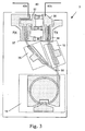
- the device constitutes a transceiver device (transceiver) 3 ( Fig.3 ), resulting from the combination of the devices 1 and 2 ( Fig.1 , Fig.2 ), as described, and comprises an antenna 40, a laser 13, a first photodiode 17 connected to the antenna 40 and used to transmit the modulated signal and a second photodiode 27 connected to the same antenna and used to receive the modulated millimetre wave signal.
- the first photodiode 17 and the second photodiode 27 are connected to the laser 13, respectively, by means of a first amplifier circuit 15 and a second amplifier 25 and a coupler 50 that allows to insert the signal generated by the laser 13 both in the first photodiode 17 and in the second photodiode 27.
- a photo-generated current is generated at a frequency corresponding to the selected millimetre wavelength, with superposed the modulating signal obtained by varying the gain of the amplifier 15. Said current is used as the driving current of the antenna.
- the photo-generated at the frequency of the millimetre wave carrier is used to move to the base band the signal received through the antenna through an electrical beat obtained by means of the non linear characteristic of the photodiode made to operate simultaneously also as a mixer diode, by means of appropriate bias applied through the contacts 38 and 39 as described previously for the receiver of Figure 2 .
- a device having a resistor bridge electrical arrangement ( Fig.4 ) is proposed herein as a preferred embodiment.
- couplers or circulators for millimetre waves.
- the first photodiode 17 ( Fig.3 , Fig. 4 ) and the second photodiode 27 are positioned on opposite diagonals of the resistor bridge comprising respective resistors 32, 34, 36, each having characteristic impedance equal to that of the antenna 40.
- the photodiodes 17 and 27 are connected to the same antenna 40 (which operates both in transmission and reception), but the exchange of the signals between the first photodiode (transmission photodiode) 17 and the second photodiode (reception photodiode) 27 is nil, as will be readily apparent to a person versed in the art.
- the transceiver 3 comprises, in addition to the circuit elements described above, for the transmitter 1 and the receiver 2, the resistors 32, 34, 36 in which the resistor 32 is connected between the anode of the photodiode 17 and the anode of the photodiode 27, the resistor 34 is connected between the anode of the photodiode 17 and the cathode of the photodiode 27 and the resistor 36 is connected between the cathode of the photodiode 17 and the cathode of the photodiode 28.
- the disposition of the resistors is optimised to reduce the distance between the contacts to be connected in order to reduce the effect of parasitic capacities.
- the transceiver 3 is, therefore, able both to transmit and to receive useful information and, therefore, it can be used, for example, as a basic circuit element for a transceiver electronic module (module) 5 ( Fig. 5 ) in a wireless millimetre wave local area network (local area network), as described in detail hereafter.
- the transceiver device 3 can be used alternatively to transmit and receive non modulated millimetre waves, simply not applying modulation signals to the first amplifier 15 and revealing only the millimetre waves at the ends of the second photodiode 27.
- the module 5 comprises a first electronic circuitry 60, of a known type, connected in input, to the contacts 16a and 10a of the amplifier 15 of the transceiver 3 and able to generate, on the basis of useful information to be transmitted, a modulating signal I e (IN-MOD) to be transmitted superposed to the millimetric carrier.
- the module 5 comprise a second electronic circuitry 70, of known fashion, connected in output, to the contacts 31 and 37 of the receiving photodiode of the transceiver 3 and able to process the output signal (OUT-MOD) implementing the function of extracting the useful information based on the expression [10]; in other words, the electronic circuitry 70 is able to reconstruct or demodulate the useful information, based on the output signal (OUT-MOD) from the transceiver 3.
- OUT-MOD output signal
- the transmitter 1 and the receiver 2 can be used to obtain a wireless local area network, as is readily apparent to a person versed in the art.
- the devices and modules according to the present invention have been described taking as a reference millimetric waves in the frequency range between 30 and 300 GHz, but nothing prevents the extension of their use both to lower frequencies, range in which said solution could be uneconomical, and to higher frequencies, range in which current technological limitations and the lack of adequate measuring instrumentation prevent a punctual certification.
Landscapes
- Physics & Mathematics (AREA)
- Electromagnetism (AREA)
- Optical Communication System (AREA)
- Radar Systems Or Details Thereof (AREA)
- Transceivers (AREA)
- Processing And Handling Of Plastics And Other Materials For Molding In General (AREA)
- Transmitters (AREA)
Claims (17)
- Zum Empfang von Millimeterwellen geeignete integrierte Einrichtung, mit:- einer zur Erzeugung optischer Signale geeigneten Laserschaltung (13);- einer mit der Laserschaltung (13) mittels eines Wellenleiters (20) verbundenen Fotodiodenschaltung (27), wobei die optischen Signale in der Fotodiodenschaltung einem optischen Takt unterworfen sind, wodurch erste Millimeterwellensignale erzeugt werden;- zum Empfang von zweiten Millimeterwellensignalen geeigneten Antennenanschlüssen (40a, 40b);wobei- die Laserschaltung, die Fotodiodenschaltung und der Wellenleiter auf einem Substrat (18) integriert sind;- die Antennenanschlüsse mit der Fotodiodenschaltung durch Kontaktelemente (19, 21) der Fotodiodenschaltung verbunden sind, so dass die zweiten Millimeterwellensignale der Fotodiodenschaltung über die Kontaktelemente zugeführt und mit den ersten Millimeterwellensignalen gemischt werden, um einen elektrischen Takt zwischen dem ersten und dem zweiten Millimeterwellensignal in der Fotodiodenschaltung zu verursachen.
- Integrierte Einrichtung nach Anspruch 1, dadurch gekennzeichnet, dass das Substrat aus einem Halbleitermaterial hergestellt ist.
- Integrierte Einrichtung nach Anspruch 2, dadurch gekennzeichnet, dass das Halbleitermaterial Gallium-Arsenid oder Indium-Phosphit enthält.
- Integrierte Einrichtung nach einem der Ansprüche 1 bis 3, dadurch gekennzeichnet, dass
die Laserschaltung einen Laserleiter (12) vom Ring-Typ enthält. - Integrierte Einrichtung nach Anspruch 4, dadurch gekennzeichnet, dass
die Laserschaltung geeignet ist, in passiver Modenverriegelung zu arbeiten. - Integrierte Einrichtung nach Anspruch 5, dadurch gekennzeichnet, dass
die Laserschaltung einen sättigbaren Absorptionsbereich (12a) enthält. - Integrierte Einrichtung nach einem der Ansprüche 1 bis 6, dadurch gekennzeichnet, dass
die zweiten Millimeterwellensignale eine modulierende Komponente enthalten und die Kontaktelemente (19, 21) geeignet sind, als eine Folge des elektrischen Takts zwischen dem ersten und zweiten Millimeterwellensignal in der Fotodiodenschaltung eine Extraktion der modulierenden Komponente zu erlauben. - Integrierte Einrichtung nach einem der Ansprüche 1 bis 7, wobei die integrierte Einrichtung weiterhin zum Senden von Millimeterwellen geeignet ist, dadurch gekennzeichnet, dass
sie eine weitere Fotodiodenschaltung (27) enthält, die mit den Antennenelementen verbunden ist. - Integrierte Einrichtung nach Anspruch 8, dadurch gekennzeichnet, dass
die weitere Fotodiodenschaltung mit der Laserschaltung mittels eines weiteren Wellenleiters verbunden ist. - Integrierte Einrichtung nach Anspruch 9, dadurch gekennzeichnet, dass
der weitere Wellenleiter mit einer ersten Verstärkerschaltung (15) verbunden ist. - Integrierte Einrichtung nach Anspruch 10, dadurch gekennzeichnet, dass
der Wellenleiter mit einer zweiten Verstärkerschaltung (25) verbunden ist. - Integrierte Einrichtung nach einem der Ansprüche 8 bis 11, dadurch gekennzeichnet, dass
die Laserschaltung einen Koppler (50) enthält, der die Laserschaltung jeweils mit dem Wellenleiter und dem weiteren Wellenleiter verbinden kann. - Modul zum Empfang von Millimeterwellen, mit:- einer integrierten Einrichtung nach Anspruch 7;- einer mit den Kontaktelementen verbundenen elektronischen Schaltung (70), die die modulierende Komponente erfassen kann.
- Modul zum Senden und Empfang von Millimeterwellen, mit:- einer integrierten Einrichtung nach Anspruch 10 oder 11;- einer mit der ersten Verstärkerschaltung (15) verbundenen ersten elektronischen Schaltung, die ein modulierendes Signal erzeugen kann, das den zu sendenden Millimeterwellen überlagert wird;- einer mit den Kontaktelementen verbundenen zweiten elektronischen Schaltung (70), die die den empfangenen Millimeterwellen überlagerte modulierende Komponente erfassen kann.
- Modul nach Anspruch 13 oder 14, dadurch gekennzeichnet, dass
es weiterhin ein mit den Kontaktelementen verbundenes Vorspannungselement enthält, das geeignet ist, eine Vorspannung an die Fotodiodenschaltung anzulegen. - Modul nach Anspruch 14, dadurch gekennzeichnet, dass
das den zu sendenden Millimeterwellen zu überlagernde modulierende Signal ein analoges Signal ist. - Modul nach Anspruch 14, dadurch gekennzeichnet, dass
das den zu sendenden Millimeterwellen zu überlagernde modulierende Signal ein digitales Signal ist.
Applications Claiming Priority (1)
| Application Number | Priority Date | Filing Date | Title |
|---|---|---|---|
| PCT/IT2002/000414 WO2004001955A1 (en) | 2002-06-21 | 2002-06-21 | Millimeter wave transmitter using optrical heterodyning |
Publications (2)
| Publication Number | Publication Date |
|---|---|
| EP1516428A1 EP1516428A1 (de) | 2005-03-23 |
| EP1516428B1 true EP1516428B1 (de) | 2008-03-12 |
Family
ID=29798527
Family Applications (1)
| Application Number | Title | Priority Date | Filing Date |
|---|---|---|---|
| EP02772802A Expired - Lifetime EP1516428B1 (de) | 2002-06-21 | 2002-06-21 | Millimeterwellensender unter verwendung von einem optischen mischer , und verfahren dazu |
Country Status (7)
| Country | Link |
|---|---|
| US (1) | US7542682B2 (de) |
| EP (1) | EP1516428B1 (de) |
| JP (1) | JP4444103B2 (de) |
| AT (1) | ATE389260T1 (de) |
| AU (1) | AU2002337609A1 (de) |
| DE (1) | DE60225601T2 (de) |
| WO (1) | WO2004001955A1 (de) |
Families Citing this family (8)
| Publication number | Priority date | Publication date | Assignee | Title |
|---|---|---|---|---|
| RU2382507C2 (ru) | 2004-04-14 | 2010-02-20 | Телеком Италия С.П.А. | Способ и система для распределения мультимедийного содержимого посредством сети беспроводной связи, в частности сети мобильной телефонной связи |
| DE102006058395B4 (de) * | 2006-12-07 | 2012-05-16 | Fraunhofer-Gesellschaft zur Förderung der angewandten Forschung e.V. | Anordnung zur elektrischen Ansteuerung und schnellen Modulation von THz-Sendern und THz-Messsystemen |
| KR101385108B1 (ko) * | 2009-12-17 | 2014-04-29 | 한국전자통신연구원 | 포토믹서 모듈 및 그것의 테라헤르츠파 발생 방법 |
| EP2523369A1 (de) * | 2011-05-12 | 2012-11-14 | Mikko Väänänen | Breitbandbasisstation mit Vorrichtung zur optischen Freiraum-Kommunikation |
| US9146133B2 (en) | 2011-06-06 | 2015-09-29 | Honeywell International Inc. | Methods and systems for displaying procedure information on an aircraft display |
| JP2013162149A (ja) * | 2012-02-01 | 2013-08-19 | Sony Corp | 伝送方法、及び、伝送システム |
| US10291286B2 (en) * | 2017-09-06 | 2019-05-14 | At&T Intellectual Property I, L.P. | Method and apparatus for guiding an electromagnetic wave to a transmission medium |
| US12615066B2 (en) * | 2022-04-07 | 2026-04-28 | Apple Inc. | Electronic devices with power boosting for high frequency communication |
Family Cites Families (12)
| Publication number | Priority date | Publication date | Assignee | Title |
|---|---|---|---|---|
| US4156135A (en) * | 1976-11-11 | 1979-05-22 | The United States Of America As Represented By The Secretary Of The Army | Electronic heterodyning in an optical detector |
| US4759081A (en) * | 1984-04-26 | 1988-07-19 | Alcatel N.V. | Optical receiver |
| US5029306A (en) * | 1989-08-10 | 1991-07-02 | The Boeing Company | Optically fed module for phased-array antennas |
| US5307073A (en) | 1992-11-13 | 1994-04-26 | General Electric Co. | Optically controlled phased array radar |
| US5379309A (en) * | 1993-08-16 | 1995-01-03 | California Institute Of Technology | High frequency source having heterodyned laser oscillators injection-locked to a mode-locked laser |
| JP2870632B2 (ja) * | 1995-07-13 | 1999-03-17 | 日本電気株式会社 | 半導体光集積回路およびその製造方法 |
| US5710651A (en) * | 1995-12-13 | 1998-01-20 | California Institute Of Technology | Remote millimeter-wave antenna fiber optic communication system using dual optical signal with millimeter-wave beat frequency |
| DE19710033C1 (de) * | 1997-03-12 | 1998-04-23 | Univ Dresden Tech | Verfahren zur Umsetzung der Signalmodulation der Kanäle eines optischen Multiplex-Systems auf Subcarrierfrequenzen |
| US5998781A (en) * | 1997-04-30 | 1999-12-07 | Sandia Corporation | Apparatus for millimeter-wave signal generation |
| US6348683B1 (en) * | 1998-05-04 | 2002-02-19 | Massachusetts Institute Of Technology | Quasi-optical transceiver having an antenna with time varying voltage |
| US6211996B1 (en) * | 1999-05-19 | 2001-04-03 | Matsushita Electric Industrial Co., Ltd. | Angle modulator |
| US6175672B1 (en) | 1999-06-18 | 2001-01-16 | Raytheon Company | RF wide bandwidth lossless high performance low noise transmissive link |
-
2002
- 2002-06-21 WO PCT/IT2002/000414 patent/WO2004001955A1/en not_active Ceased
- 2002-06-21 DE DE60225601T patent/DE60225601T2/de not_active Expired - Lifetime
- 2002-06-21 JP JP2004515422A patent/JP4444103B2/ja not_active Expired - Fee Related
- 2002-06-21 EP EP02772802A patent/EP1516428B1/de not_active Expired - Lifetime
- 2002-06-21 AT AT02772802T patent/ATE389260T1/de not_active IP Right Cessation
- 2002-06-21 AU AU2002337609A patent/AU2002337609A1/en not_active Abandoned
- 2002-06-21 US US10/519,771 patent/US7542682B2/en not_active Expired - Fee Related
Also Published As
| Publication number | Publication date |
|---|---|
| DE60225601T2 (de) | 2009-04-02 |
| JP4444103B2 (ja) | 2010-03-31 |
| AU2002337609A1 (en) | 2004-01-06 |
| EP1516428A1 (de) | 2005-03-23 |
| DE60225601D1 (de) | 2008-04-24 |
| ATE389260T1 (de) | 2008-03-15 |
| WO2004001955A1 (en) | 2003-12-31 |
| US20050259908A1 (en) | 2005-11-24 |
| JP2005530452A (ja) | 2005-10-06 |
| US7542682B2 (en) | 2009-06-02 |
Similar Documents
| Publication | Publication Date | Title |
|---|---|---|
| Nagatsuma et al. | Recent progress and future prospect of photonics-enabled terahertz communications research | |
| Gliese et al. | Multifunctional fiber-optic microwave links based on remote heterodyne detection | |
| Stöhr et al. | Millimeter-wave photonic components for broadband wireless systems | |
| US5917636A (en) | Generation of radio frequency modulated optical radiation | |
| Braun et al. | Optical microwave generation and transmission experiments in the 12-and 60-GHz region for wireless communications | |
| Tsuchiya et al. | Nonlinear photodetection scheme and its system applications to fiber-optic millimeter-wave wireless down-links | |
| Ito et al. | Rectangular waveguide output unitraveling-carrier photodiode module for high-power photonic millimeter-wave generation in the F-band | |
| EP1516428B1 (de) | Millimeterwellensender unter verwendung von einem optischen mischer , und verfahren dazu | |
| Nagatsuma et al. | 600-GHz-band waveguide-output uni-traveling-carrier photodiodes and their applications to wireless communication | |
| CN101674136B (zh) | OFDM调制方式的光学倍频毫米波RoF信号生成系统及方法 | |
| Liu et al. | Two-terminal edge-coupled InP/InGaAs heterojunction phototransistor optoelectronic mixer | |
| Ogawa et al. | Fiber optic microwave links using balanced laser harmonic generation, and balanced/image cancellation laser mixing | |
| CN114124235B (zh) | 模拟光子链路 | |
| Lacombe et al. | 300 GHz OOK transmitter integrated in advanced silicon photonics technology and achieving 20 Gb/s | |
| Wake et al. | Optoelectronics for millimetre-wave radio over fibre systems | |
| Nagatsuma et al. | Photonics-Based Transmitters and Receivers | |
| JPH05206987A (ja) | モードロックダイオードレーザ及びそれを用いた光通信システム | |
| Daryoush et al. | Efficient optoelectronic mixing at Ka-band using a mode-locked laser | |
| Liu et al. | Fiber-optic microwave link with monolithic integrated optoelectronic up-converter | |
| Kang et al. | CMOS-compatible 60 GHz harmonic optoelectronic mixer | |
| Wenke et al. | Stabilised PSK transmitter with negative electrical feedback to a semiconductor laser | |
| Seeds | Microwave opto-electronics: principles, applications and future prospects | |
| Piotrowski et al. | Investigation of InGaAs pin photodiode for optical-microwave mixing process | |
| Wun et al. | THz Photonic Transmitters with Type-II Hybrid Absorber UTC-PDs and Dual-Ridged Horn Antennas for High-Power and Extremely wide Fractional Bandwidth Performances | |
| Johnson et al. | CW operation of folded-cavity semiconductor lasers with etched turning mirrors |
Legal Events
| Date | Code | Title | Description |
|---|---|---|---|
| PUAI | Public reference made under article 153(3) epc to a published international application that has entered the european phase |
Free format text: ORIGINAL CODE: 0009012 |
|
| 17P | Request for examination filed |
Effective date: 20041214 |
|
| AK | Designated contracting states |
Kind code of ref document: A1 Designated state(s): AT BE CH CY DE DK ES FI FR GB GR IE IT LI LU MC NL PT SE TR |
|
| AX | Request for extension of the european patent |
Extension state: AL LT LV MK RO SI |
|
| DAX | Request for extension of the european patent (deleted) | ||
| GRAP | Despatch of communication of intention to grant a patent |
Free format text: ORIGINAL CODE: EPIDOSNIGR1 |
|
| RTI1 | Title (correction) |
Free format text: MILLIMETER WAVE TRANSMITTER USING OPTICAL HETERODYNING |
|
| GRAS | Grant fee paid |
Free format text: ORIGINAL CODE: EPIDOSNIGR3 |
|
| GRAA | (expected) grant |
Free format text: ORIGINAL CODE: 0009210 |
|
| AK | Designated contracting states |
Kind code of ref document: B1 Designated state(s): AT BE CH CY DE DK ES FI FR GB GR IE IT LI LU MC NL PT SE TR |
|
| REG | Reference to a national code |
Ref country code: GB Ref legal event code: FG4D |
|
| REG | Reference to a national code |
Ref country code: CH Ref legal event code: EP |
|
| REG | Reference to a national code |
Ref country code: IE Ref legal event code: FG4D |
|
| REF | Corresponds to: |
Ref document number: 60225601 Country of ref document: DE Date of ref document: 20080424 Kind code of ref document: P |
|
| RAP2 | Party data changed (patent owner data changed or rights of a patent transferred) |
Owner name: TELECOM ITALIA S.P.A. |
|
| PG25 | Lapsed in a contracting state [announced via postgrant information from national office to epo] |
Ref country code: FI Free format text: LAPSE BECAUSE OF FAILURE TO SUBMIT A TRANSLATION OF THE DESCRIPTION OR TO PAY THE FEE WITHIN THE PRESCRIBED TIME-LIMIT Effective date: 20080312 |
|
| PG25 | Lapsed in a contracting state [announced via postgrant information from national office to epo] |
Ref country code: AT Free format text: LAPSE BECAUSE OF FAILURE TO SUBMIT A TRANSLATION OF THE DESCRIPTION OR TO PAY THE FEE WITHIN THE PRESCRIBED TIME-LIMIT Effective date: 20080312 |
|
| NLV1 | Nl: lapsed or annulled due to failure to fulfill the requirements of art. 29p and 29m of the patents act | ||
| PG25 | Lapsed in a contracting state [announced via postgrant information from national office to epo] |
Ref country code: BE Free format text: LAPSE BECAUSE OF FAILURE TO SUBMIT A TRANSLATION OF THE DESCRIPTION OR TO PAY THE FEE WITHIN THE PRESCRIBED TIME-LIMIT Effective date: 20080312 |
|
| PG25 | Lapsed in a contracting state [announced via postgrant information from national office to epo] |
Ref country code: ES Free format text: LAPSE BECAUSE OF FAILURE TO SUBMIT A TRANSLATION OF THE DESCRIPTION OR TO PAY THE FEE WITHIN THE PRESCRIBED TIME-LIMIT Effective date: 20080623 Ref country code: SE Free format text: LAPSE BECAUSE OF FAILURE TO SUBMIT A TRANSLATION OF THE DESCRIPTION OR TO PAY THE FEE WITHIN THE PRESCRIBED TIME-LIMIT Effective date: 20080612 Ref country code: PT Free format text: LAPSE BECAUSE OF FAILURE TO SUBMIT A TRANSLATION OF THE DESCRIPTION OR TO PAY THE FEE WITHIN THE PRESCRIBED TIME-LIMIT Effective date: 20080818 |
|
| PG25 | Lapsed in a contracting state [announced via postgrant information from national office to epo] |
Ref country code: NL Free format text: LAPSE BECAUSE OF FAILURE TO SUBMIT A TRANSLATION OF THE DESCRIPTION OR TO PAY THE FEE WITHIN THE PRESCRIBED TIME-LIMIT Effective date: 20080312 |
|
| ET | Fr: translation filed | ||
| PLBE | No opposition filed within time limit |
Free format text: ORIGINAL CODE: 0009261 |
|
| STAA | Information on the status of an ep patent application or granted ep patent |
Free format text: STATUS: NO OPPOSITION FILED WITHIN TIME LIMIT |
|
| PG25 | Lapsed in a contracting state [announced via postgrant information from national office to epo] |
Ref country code: MC Free format text: LAPSE BECAUSE OF NON-PAYMENT OF DUE FEES Effective date: 20080630 Ref country code: DK Free format text: LAPSE BECAUSE OF FAILURE TO SUBMIT A TRANSLATION OF THE DESCRIPTION OR TO PAY THE FEE WITHIN THE PRESCRIBED TIME-LIMIT Effective date: 20080312 |
|
| REG | Reference to a national code |
Ref country code: CH Ref legal event code: PL |
|
| 26N | No opposition filed |
Effective date: 20081215 |
|
| PG25 | Lapsed in a contracting state [announced via postgrant information from national office to epo] |
Ref country code: IE Free format text: LAPSE BECAUSE OF NON-PAYMENT OF DUE FEES Effective date: 20080623 |
|
| PG25 | Lapsed in a contracting state [announced via postgrant information from national office to epo] |
Ref country code: CH Free format text: LAPSE BECAUSE OF NON-PAYMENT OF DUE FEES Effective date: 20080630 Ref country code: LI Free format text: LAPSE BECAUSE OF NON-PAYMENT OF DUE FEES Effective date: 20080630 |
|
| PG25 | Lapsed in a contracting state [announced via postgrant information from national office to epo] |
Ref country code: CY Free format text: LAPSE BECAUSE OF FAILURE TO SUBMIT A TRANSLATION OF THE DESCRIPTION OR TO PAY THE FEE WITHIN THE PRESCRIBED TIME-LIMIT Effective date: 20080312 |
|
| PG25 | Lapsed in a contracting state [announced via postgrant information from national office to epo] |
Ref country code: LU Free format text: LAPSE BECAUSE OF NON-PAYMENT OF DUE FEES Effective date: 20080621 |
|
| PG25 | Lapsed in a contracting state [announced via postgrant information from national office to epo] |
Ref country code: TR Free format text: LAPSE BECAUSE OF FAILURE TO SUBMIT A TRANSLATION OF THE DESCRIPTION OR TO PAY THE FEE WITHIN THE PRESCRIBED TIME-LIMIT Effective date: 20080312 |
|
| PG25 | Lapsed in a contracting state [announced via postgrant information from national office to epo] |
Ref country code: GR Free format text: LAPSE BECAUSE OF FAILURE TO SUBMIT A TRANSLATION OF THE DESCRIPTION OR TO PAY THE FEE WITHIN THE PRESCRIBED TIME-LIMIT Effective date: 20080613 |
|
| REG | Reference to a national code |
Ref country code: FR Ref legal event code: PLFP Year of fee payment: 15 |
|
| REG | Reference to a national code |
Ref country code: FR Ref legal event code: PLFP Year of fee payment: 16 |
|
| REG | Reference to a national code |
Ref country code: FR Ref legal event code: PLFP Year of fee payment: 17 |
|
| PGFP | Annual fee paid to national office [announced via postgrant information from national office to epo] |
Ref country code: IT Payment date: 20190621 Year of fee payment: 18 |
|
| PGFP | Annual fee paid to national office [announced via postgrant information from national office to epo] |
Ref country code: FR Payment date: 20190625 Year of fee payment: 18 |
|
| PGFP | Annual fee paid to national office [announced via postgrant information from national office to epo] |
Ref country code: DE Payment date: 20190627 Year of fee payment: 18 Ref country code: GB Payment date: 20190627 Year of fee payment: 18 |
|
| REG | Reference to a national code |
Ref country code: DE Ref legal event code: R119 Ref document number: 60225601 Country of ref document: DE |
|
| GBPC | Gb: european patent ceased through non-payment of renewal fee |
Effective date: 20200621 |
|
| PG25 | Lapsed in a contracting state [announced via postgrant information from national office to epo] |
Ref country code: FR Free format text: LAPSE BECAUSE OF NON-PAYMENT OF DUE FEES Effective date: 20200630 Ref country code: GB Free format text: LAPSE BECAUSE OF NON-PAYMENT OF DUE FEES Effective date: 20200621 |
|
| PG25 | Lapsed in a contracting state [announced via postgrant information from national office to epo] |
Ref country code: DE Free format text: LAPSE BECAUSE OF NON-PAYMENT OF DUE FEES Effective date: 20210101 |
|
| PG25 | Lapsed in a contracting state [announced via postgrant information from national office to epo] |
Ref country code: IT Free format text: LAPSE BECAUSE OF NON-PAYMENT OF DUE FEES Effective date: 20200621 |