BACKGROUND OF THE INVENTION
[Field of the Invention]
-
The present invention relates to an organic
electroluminescence device whose luminous region is
substantially rectangular.
[Description of the Related Art]
-
Electrodes of an organic electroluminescence device have
various restrictions such as a restriction that at least one
electrode must have optical transparency, and a restriction
that electrodes must be constituted by a material and
production method which do not deteriorate an organic layer,
and the like. Therefore, the material adoptable as electrodes
of an organic electroluminescence device is limited extremely.
-
In addition, since an apparatus (for example, personal
digital assistant etc.) equipped with an organic
electroluminescence device has a limit in its size, the size
of the device concerned also has restrictions. In
consequence, the size and located positions of terminal
sections of electrodes are also limited.
-
As a result, in plenty of respective current paths in
which currents in the organic electroluminescence device flow,
those resistances may largely differ. For this reason, for
example, the following problems have occurred.
• Occurrence of brightness unevenness
-
Since locations where rich currents flow and locations
where poor currents flow exist, brightness unevenness occurs
as the entire device. This is because, since the luminance of
the organic electroluminescence device becomes high as a
flowing current becomes large, the difference of luminance
occurs between both to become brightness unevenness, when a
location where a rich current flows and a location where a
poor current flows exist.
• Occurrence of lifetime difference in device
-
The lifetimes in a device differ in a location through
which a rich current flows, and a location through which a
poor current flows. Generally, a lifetime of a portion
through which a rich current flows becomes short. For this
reason, a location, which has a short lifetime in comparison
with a device where a uniform current flows, exists, and
hence, a lifetime as the organic electroluminescence device
becomes short. In addition, when an organic
electroluminescence device is used for a long time, a location
not shining arises or a location whose luminance is lower than
that of other locations arises.
• Problems such as deterioration
-
Since a location through which a rich current flows and a
location through which a poor current flows exist, a location
being deteriorated may arise.
• Occurrence of chromaticity unevenness
-
Since there are a location through which a rich current
flows and a location through which a poor current flows, in a
device, an S-S annihilation phenomenon arises in the case of
an organic electroluminescence device using a fluorescent
material, or a T-T annihilation phenomenon arises in the case
of an organic electroluminescence device using a
phosphorescence material. Hence, in an organic
electroluminescence device which contains a plurality of
luminescent materials in its luminescent layer, and in which
each luminescent material emits a color with a wavelength
different from at least one other luminescent material, it may
arise that the luminance of each layer differs from others at
a location where a current is easy to flow and a location
where a current is hard to flow. As a result, the
chromaticity unevenness may arise.
-
As for these problems, their advantages could be made
small if, for example, it were possible to produce an organic
electroluminescence device only with materials having small
volume resistivity values, or a terminal section over the
entire circumference of the device could be provided. But,
since there are various restrictions as described above, they
have actually arisen.
-
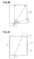
Hereinafter, resistance difference between respective
paths, in which currents flow, in an organic
electroluminescence device will be explained in detail by
using FIG. 26.
-
In the organic electroluminescence device used for
explanation here, an electrode provided in an optical output
side rather than an organic layer is an anode formed of ITO,
and a cathode, which faces the anode, is formed of aluminum.
In this structure, since the volume resistivity of aluminum is
very small in comparison with that of ITO, its volume
resistivity can be disregarded substantially. Hence, only the
anode which poses a problem (which is an electrode with high
volume resistivity) at the time of considering the resistance
difference between respective paths is shown in FIG. 26.
-
An anode 100 includes a terminal section 110 to which an
external drive circuit is connected, and a region (electrode
region) 130, which contacts an organic layer. A region
adjacent to the electrode region 130 in the organic layer
becomes a region (luminous region) which a current is flowed
in and emits light.
-
In order to eliminate problems such as brightness
unevenness in the luminous region of the organic
electroluminescence device with this structure, resistances
from a point P0, at which the terminal section 110 contacts to
the electrode region 130, on an electrode region 130 to
respective points on the electrode region 130, for example, P1
to P6 must be equal.
-
Nevertheless, the volume resistivity of ITO is not such a
small value that it can be ignored when the resistances of
respective current paths in the organic electroluminescence
device is considered. Hence, a resistance is small in a path,
in which the distance of passing through ITO is short, such as
the current path between P0 and P1, P2, or P3, and a
resistance becomes large in a path, in which the distance of
passing through ITO is long, such as the current path between
P0 and P4, P5, or P6. Hence, the magnitude of a current which
flows through the organic layer differs by a path, that is, a
position in the luminous region, and as a result, brightness
unevenness and the like arise.
-
FIG. 27 shows an organic electroluminescence device in
which an anode and a cathode are formed of ITO. In this
figure, a continuous line shows the anode, and a doted line
shows the cathode. A cathode 300 includes a terminal section
310 to which an external drive circuit is connected, and a
region (electrode region) 330, which contacts an organic
layer.
-
In this organic electroluminescence device, since both
electrodes are formed of ITO, both of the resistivity of the
anode and the resistivity of the cathode cannot be ignored
when the resistance difference between the above-mentioned
respective paths is considered.
-
In this structure, the resistance of the path of passing
through a path (minimum distance) L1 connecting the terminal
sections 110 and 310 with a straight line becomes the
smallest. Hence, the current, which flows in the organic
layer on the path L1, becomes the largest and the current,
which flows in the organic layer, becomes small as a path is
apart from the path L1. As a result, brightness unevenness
and the like arise.
-
Various types of prior art are proposed as prior art,
which cancels brightness unevenness. For example, an
electroluminescence device is also proposed, the device which
includes a luminescent layer which is provided between first
and second electrodes, and has a luminous region which emits
light in the luminance corresponding to a voltage between the
above-described first and second electrodes and its thickness,
the above-mentioned luminescent layer which has the thickness
of differing in a layer thickness direction so that the
luminance of the luminous region may become uniform (for
example, see Japanese Patent Laid-Open No. 11-40362
publication). The above-mentioned first electrode has a first
terminal for applying a voltage, and the second electrode is
provided with facing the first electrode, has a second
terminal for applying a voltage, and exhibits a sheet
resistance lower than that of the above-mentioned first
electrode.
SUMMARY OF THE INVENTION
-
An object of the present invention is to lessen the
difference of magnitude between currents flowing at respective
positions in a luminous region in an organic
electroluminescence device. Thus, it is to lessen the
difference of resistances between respective current paths,
which exist in the organic electroluminescence device
innumerably.
-
To achieve the above-mentioned objective, the present
invention provides an organic electroluminescent device. The
device includes a first electrode, a second electrode that is
formed of a material the volume resistivity of which is equal
to or higher than the volume resistivity of the first
electrode, and an organic layer between the first electrode
and the second electrode. The second electrode includes a
substantially rectangular electrode region that contacts the
organic layer, a terminal section to which an external drive
circuit is connected, wherein the terminal section is located
in a predetermined position along the outer periphery of the
electrode region, and a conductive section that electrically
connects the terminal section to the electrode region. The
conductive section includes a first joint connected to the
terminal section, a second joint connected to the outer
periphery of the electrode region, and a conductive section
main body that extends between the first joint and the second
joint to electrically connect the first joint to the second
joint.
-
Other aspects and advantages of the invention will become
apparent from the following description, taken in conjunction
with the accompanying drawings, illustrating by way of example
the principles of the invention.
BRIEF DESCRIPTION OF THE DRAWINGS
-
The invention, together with objects and advantages
thereof, may best be understood by reference to the following
description of the presently preferred embodiments together
with the accompanying drawings in which:
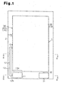
- FIG. 1 is a top view of a first organic EL device, which
embodied the present invention;
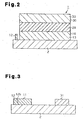
- FIG. 2 is a sectional view taken on line A-A' in FIG. 1;
- FIG. 3 is a sectional view taken on line B-B' in FIG. 1;
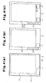
- FIGS. 4(a) to 4(c) are top views for explaining a
production method of the organic EL device shown in FIG. 1;
- FIG. 5(a) is a top view of an anode of the organic EL
device shown in FIG. 1;
- FIG. 5(b) is a top view of an anode of a conventional
organic EL device;
- FIGS. 6(a) and 6(b) each is a schematic top view of an
anode of a modified example where a conductive section
differs;
- FIGS. 7(a) and 7(b) each is a schematic top view of an
anode of a modified example where a conduction section
differs;
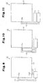
- FIG. 8 is a schematic top view of an anode of a modified
example where a conductive section differs;
- FIG. 9 is a top view of an anode of another modified
example;
- FIG. 10 is a schematic top view of an anode of a modified
example having a highly resistive section;
- FIG. 11 is a schematic top view of an anode of a modified
example having a highly resistive section;
- FIGS. 12(a) to 12(c) each is a schematic top view of an
anode of a modified example where a conductive section
differs;
- FIG. 13 is a schematic top view of an anode of a modified
example where a position of a terminal section differs;
- FIGS. 14(a) and 14(b) each is a top view of a modified
example of an electrode region of an anode;
- FIG. 15 is a schematic top view of an anode of a modified
example where a position of a terminal section differs;
- FIG. 16 is a top view of an anode of another modified
example;
- FIG. 17 is a schematic exploded perspective view of an.
organic EL device having an insulated section;
- FIG. 18 is a schematic sectional view of the organic EL
device having the insulated section;
- FIG. 19 is a schematic top view showing the arrangement
of an electrode region, a terminal section, etc. of an anode
on a substrate;
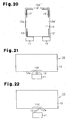
- FIG. 20 is a schematic top view of an anode of a second
organic EL device, which embodied the present invention;
- FIG. 21 is a schematic top view of an anode of a modified
example where a position of a terminal section differs;
- FIG. 22 is a schematic top view of an anode of a modified
example where a position of a terminal area differs;
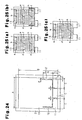
- FIGS. 23(a) and 23(b) each is a top view of an anode
formed by combining the first and second organic EL devices;
- FIG. 24 is a schematic top view showing dimensions of an
electrode region, a terminal section, etc. of an anode;
- FIG. 25(a) is a schematic diagram showing luminance
measurement points of an example 1;
- FIG. 25(b) is a schematic diagram showing luminance
measurement points of an example 2;
- FIG. 25(c) is a schematic diagram showing luminance
measurement points of a comparative example;
- FIG. 26 is a schematic diagram for explaining resistance
difference between respective paths, in which currents flow,
in an organic electroluminescence device; and
- FIG. 27 is a schematic diagram for explaining resistance
difference between respective paths, in which currents flow,
in the organic electroluminescence device shown in FIG. 26.
-
DETAILED DESCRIPTION OF THE PREFERRED EMBODIMENTS
-
Hereinafter, an organic electroluminescence device
(hereinafter, this is described as an organic EL device),
which embodied the present invention will be explained in
detail. First, a first organic EL device will be explained.
The first organic EL device, which relates to the present
invention has the following features.
- One electrode (in this example, an anode) is formed of a
material whose volume resistivity is higher than that of
another electrode (in this example, a cathode). In other
words, when the cathode is a first electrode and the anode is
a second electrode, the second electrode is formed of a
material the volume resistivity of which is higher than the
volume resistivity of the first electrode.
- An organic layer exists between the anode and cathode.
- The anode has at least an electrode region, which contacts
an organic layer, a terminal section to which an external
drive circuit is connected, and a conductive section.
- The electrode region of the anode is substantially
rectangular.
- The terminal section is located in a position along the
outer periphery of the electrode region of the anode, and
electrically connected to the electrode region of the anode
through the conductive section of the anode.
- The conductive section of the anode includes a joint
connected to the terminal section of the anode, a joint
connected to the electrode region of the anode, and a main
body of the conductive section which electrically connects
both joints and does not electrically connect the electrode
region and terminal section of the anode.
- The joint connected to the electrode region of the anode is
connected to the electrode region of the anode in a portion
other than a portion, which faces the terminal section in the
outer periphery of the electrode region of the anode.
-
Hereinafter, the structure, a production example,
actions, and advantages of the first organic EL device will be
explained in detail with referring to figures.
<Structure>
-
As shown in FIGS. 1 to 3, the first organic EL device 1
is formed on a substrate 2. As shown in FIG. 2, the first
organic EL device 1 has an anode 10 as one electrode, an
organic layer 20, and a cathode 30 as another electrode.
Hereinafter, each component, which constitutes the first
organic EL device 1, will be explained.
(Anode 10)
-
The anode 10 has a terminal section 11 of the anode, a
conductive section 12 of the anode, and an electrode region 13
of the anode, and each is formed on the substrate 2. The
terminal section 11 of the anode, the conductive section 12 of
the anode, and the electrode region 13 of the anode are formed
in one piece with a material whose volume resistivity is
higher than that of the cathode 30 (at least electrode region
33 of the cathode). That is, the cathode 30 functions as a
first electrode and the anode 10 functions as a second
electrode that is formed of a material the volume resistivity
of which is higher than the volume resistivity of the first
electrode.
-
The terminal section 11 of the anode is provided in a
position along the outer periphery of the electrode region 13
of the anode as shown in FIG. 1, and is connected to an
external drive circuit which is not shown. It is not
necessary to connect with the external drive circuit over the
entire terminal section 11 of the anode, but a part of the
section may be also connected to the external drive circuit.
The terminal section 11 of the anode is not directly connected
to the electrode region 13 of the anode. That is, the
electrode region 13 of the anode and the terminal section 11
of the anode are separately located on the substrate 2 lest a
current should directly flow into the electrode region 13 of
the anode from the terminal section 11 of the anode.
-
The conductive section 12 of the anode electrically
connects the terminal section 11 of the anode, and the
electrode region 13 of the anode. More specifically, as shown
in FIG. 1, a first joint 12b, which is one end of the
conductive section 12, connects with the terminal section 11
of the anode, and a second joint 12a, which is another end of
the conductive section 12, connects with the electrode region
13 of the anode. Portions of the conductive section 12 except
joints 12a and 12b do not connect with the terminal section 11
of the anode, and the electrode region 13 of the anode. A
portion between both the joints 12a and 12b of the anode
becomes a main body 12c of the conductive section 12. That
is, the main body 12c of the conductive section 12 does not
connect electrically with the electrode region 13 and terminal
section 11 of the anode.
-
A position where the conductive section 12 of the anode,
and the electrode region 13 of the anode connect, that is, a
position of the second joint 12a is a position 13a along the
outer periphery of the electrode region 13 of the anode, and a
position other than a portion 13x where the electrode region
13 of the anode faces the terminal section 11 of the anode.
In other words, the portion 13x is a "facing portion". The
second joint 12a is connected to the electrode region 13 at
the "non-facing portion".
-
The electrode region 13 of the anode is a region of
contacting the organic layer 20 as shown in FIG. 2. When
making the device emit light, positive holes are transported
from the external drive circuit connected to the terminal
section 11 of the anode through the conductive section 12 of
the anode, and the electrode region 13 injects these positive
holes into the organic layer 20.
-
What is necessary as a material for forming the anode 10
is just a material which gives the above-mentioned property to
the anode 10, and generally, a known material such as metal,
an alloy, an electrically conductive compound, or a mixture of
those is selected, which is produced so that a work function
of a face (surface) which contacts with the organic layer 20
of the electrode region 13 of the anode may become 4 eV or
more.
-
As the material for forming the anode 10, the followings
can be cited, for example. They are metal oxides and metal
nitrides such as ITO (indium-tin-oxide), IZO (indium-zinc-oxide),
a tin oxide, a zinc oxide, a zinc aluminum oxide, and
a titanium nitride; metals such as gold, platinum, silver,
copper, aluminum, nickel, cobalt, lead, chromium, molybdenum,
tungsten, tantalum, and niobium; alloys of these metals and
alloys of copper iodide; conductive polymers such as poly
aniline, poly thiophene, pyrrole, polyphenylene vinylene; poly
(3-methylthiophene), andpolyphenylene sulfide.
-
When provided in an optical output side rather than the
organic layer 20, the anode 10 is set so that a transmittance
to the light to be outputted may generally become larger than
10%. When the light in a visible light region is outputted,
ITO with a high transmittance in the visible light region is
suitably used.
-
When the anode 10 is used as a reflective electrode, a
material, having the capacity of reflecting the light
outputted to the external, among the above-mentioned materials
is selected suitably, and, generally, metal, an alloy, or a
metallic compound is selected.
-
The anode 10 may be formed of only one kind of material,
which is described above, or may be formed by mixing a
plurality of materials. In addition, it may be also multiple
layer structure, which consists of two or more layers of the
same kind of composition or different kinds of composition.
-
When a resistance of the anode 10 is high, it is good to
provide a supporting electrode to lower the resistance. The
supporting electrode is an electrode formed of metal, such as
copper, chromium, aluminum, titanium, or an aluminum alloy, or
a laminated material of these being partially attached
adjacently to the anode 10.
-
Depending also on a material to be used, the film
thickness of the anode 10 is selected generally in a range of
about 5 nm to 1 µm, preferably in a range of about 10 nm to 1
µm, more preferably in a range of about 10 nm to 500 nm,
especially preferably in a range of about 10 nm to 300 nm, and
desirably in a range of 10 nm to 200 nm.
-
The anode 10 is formed by a publicly known thin-film
forming method, such as a sputtering method, an ion plating
method, a vacuum deposition method, a spin coating method, or
an electron beam evaporation method, by using such materials
as are described above.
-
In addition, it is also good to perform the UV ozone
clearing or plasma clearing of its surface.
-
In order to suppress the occurrence of a short circuit or
a defect of an organic EL device, it is good to control
surface roughness to 20 nm or less as a mean squared value by
a method of micrifying particle size, or a method of grinding
after deposition.
(Organic layer 20)
-
The organic layer 20 can be produced by a publicly known
production method since it is sufficient to adopt publicly
known layer structure and layers made of publicly known
materials in a publicly known organic electroluminescence
device.
-
That is, it is sufficient that the organic layer 20 just
achieves at least the following functions. It is also good to
make the layer laminated structure, and to make each layer
bear one of functions, or it is also good to achieve the
following functions by a single layer.
• Electron injection function
-
A function of electrons beings injected from an electrode
(cathode). Electron injection property.
• Positive hole injection function
-
A function of positive holes being injected from an
electrode (anode). Positive hole injection property.
• Carrier transport function
-
A function of carrying at least either electrons or
positive holes. Carrier transportability.
-
The function of carrying electrons is called an
electronic transport function (electronic transportability),
and the function of carrying positive holes is called a
positive hole transport function (positive hole
transportability).
• Luminescence function
-
A function of generating excitons (being in an excitation
state) by recombining electrons and carriers, which are
injected and transported, and emitting light when returning to
a ground state.
-
Hence, in the organic layer 20, a region (luminous
region) sandwiched with a face adjacent to the electrode
region 13 of the anode and a face adjacent to the electrode
region 33 of the cathode emits light by the above-mentioned
function.
-
The organic layer 20 may be constituted by providing
layers, for example, a positive hole transportation layer, a
luminescent layer, and an electron transportation layer in
order from the anode side.
-
The positive hole transportation layer is a layer, which
transports positive holes to the luminescent layer from the
anode. As a material for forming the positive hole
transportation layer, it is possible to select one from among,
for example, metal phthalocyanines such as copper
phthalocyanine and tetra (t-butyl) copper phthalocyanine, and
non-metal phthalocyanines, low molecule materials such as
aromatic amines such as a quinacridone compound, 1, 1-bis (4-di-p-tolyl
amino phenyl) cyclohexane, N, N'-diphenyl-N, N'-bis
(3-methyl phenyl)-1, 1'-biphenyl-4, 4'-diamine, N, N'-di (1-naphthyl)-N,
N'-diphenyl-1, 1'-biphenyl-4, 4'-diamine,
polymeric materials such as poly thiophene and poly aniline, a
poly thiophene oligomer material, and other existing hole
transportation materials.
-
The luminescent layer is a layer which becomes in an
excitation state by making positive holes, transported from an
anode side, and electrons transported from a cathode side
recombined, and which emits light when returning from the
excitation state to a ground state. As a material of the
luminescent layer, a fluorescent material and a
phosphorescence material are adoptable. In addition, a dopant
(a fluorescent material or a phosphorescence material) may be
contained in a host material.
-
As a material for forming the luminescent layer, it is
possible to use one from among, for example, low molecule
materials such as a 9, 10-diarylanthracene derivative, a
pyrene derivative, a coronene derivative, a perylene
derivative, a rubrene derivative, 1, 1, 4, 4-tetra-phenyl
butadiene, a tris (8-quinolate) aluminum complex, a tris (4-methyl-8-quinolate)
aluminum complex, a bis (8-quinolate) zinc
complex, a tris (4-methyl-5-trifluoro methyl-8-quinolate)
aluminum complex, a tris (4-methyl-5-cyano-8-quinolate)
aluminum complex, a bis (2-methyl-5-trifluoro methyl-8-quinolate)
[4-(4-cyanophenyl) phenolate] aluminum complex, a
bis (2-methyl-5-cyano-8-quinolate) [4-(4-cyanophenyl)
phenolate] aluminum complex, a tris (8-quinolate) scandium
complex, a bis (8-(para-tosyl) amino quinoline] zinc complex
or cadmium complex, 1, 2, 3, 4-tetraphenyl cyclopentadiene,
pentaphenyl cyclopentadiene, polly-2, 5-diheptyloxy-paraphenylene
vinylene, a coumarin system fluorescent substance, a
perylene system fluorescent substance, a pyran system
fluorescent substance, an anthrone system fluorescent
substance, a porphyrin system fluorescent substance, a
quinacridone system fluorescent substance, an N, N'-dialkyl-substituted-quinacridone
system fluorescent substance, a
naphthalimido system fluorescent substance, and an N, N'-diaryl-substituted-pyrrolopyrrole
system fluorescent
substance, polymeric materials such as polyfluorene,
polyparaphenylenevinylene, and polythiophene, and other
existing luminescent materials. When host/guest type
structure is adopted, what is necessary is just to select a
host and a guest (dopant) suitably from these materials.
-
The electron transportation layer is a layer, which
transports electrons to the luminescent layer from the
cathode. What are cited as material for forming the electron
transportation layer includes, for example, 2-(4-biphenylyl)-5-(4-t-butyl
phenyl)-1, 3, 4-oxadiazole, 2 and 5-bis (1-naphthyl)-1,
3, 4-oxadiazole, an oxadiazole derivative, a bis
(10-hydroxybenzo [h] quinolate) beryllium complex, a triazole
compound, and the like.
-
Naturally, it is also possible to provide layers, which
are adopted as a publicly known organic electroluminescence
layer, such as a buffer layer, a positive hole block layer, an
electron injection layer, and a positive hole injection layer,
in the organic layer 20. It is also possible to provide these
layers by a publicly known production method by using a
publicly known material.
(Cathode 30)
-
As shown in FIGS. 1 to 3, the cathode 30 has a terminal
section 31 of the cathode, a conductive section 32 of the
cathode, and an electrode region 33 of the cathode, and these
components are integrally formed.
-
The terminal section 31 of the cathode is provided in a
position along the outer periphery of the electrode region 33
of the cathode, and is connected to an external drive circuit,
which is not shown. It is not necessary to connect with the
external drive circuit over the entire terminal section 31 of
the cathode, but a part of the section may be also connected
to the external drive circuit. As shown in FIG. 3, the
terminal section 31 of the cathode may be also provided on the
substrate 2.
-
The conductive section 32 of the cathode is a conductive
path, which connects electrically the terminal section 31 of
the cathode; and the electrode region 33 of the cathode.
-
The electrode region 33 of the cathode is stacked on a
face of the organic layer 20 which is oppose to a face which
contacts to the electrode region 13 of the anode. When a
device is made to emit light, electrons are transported from
the external drive circuit connected to the terminal section
31 of the cathode through the conductive section 32 of the
cathode, and these electrons are injected into the organic
layer 20.
-
Since the cathode 30 has volume resistivity smaller than
the anode 10, a connecting location of the conductive section
32 and the electrode region 33 of the cathode is not limited
especially. In addition, the conductive section 32 of the
cathode may not be provided, but the terminal section 31 of
the cathode and the electrode region 33 of the cathode may be
also connected directly.
-
The cathode 30 is an electrode, which injects electrons
into the organic layer 20 (in the above-mentioned layer
structure, the electron transportation layer). In order to
make electron injection efficiency high, metal, an alloy,
electrically conductive compounds, and mixtures of these each
of which has a work function which is for example, less than
4.5 eV, generally is 4.0 eV or less, or typically is 3.7 eV or
less can be adopted as an electrode material.
-
What are cited as the above-mentioned electrode materials
are, for example, lithium, sodium, magnesium, gold, silver,
copper, aluminum, indium, calcium, tin, ruthenium, titanium,
manganese, chromium, yttrium, an aluminum-calcium alloy, an
aluminum-lithium alloy, an aluminum magnesium alloy, a
magnesium-silver alloy, a magnesium-indium alloy, a lithium-indium
alloy, a sodium-potassium alloy, a magnesium/copper
mixture, an aluminum/aluminum oxide mixture, and the like. In
addition, it is possible to use the materials adoptable as
materials used for the anode.
-
When provided in the optical output side rather than the
luminescent layer, the cathode 30 is set so that the
transmittance to light to be outputted may generally become
larger than 10%. For example, an electrode or the like which
is formed by stacking a transparent conductive oxide on a
super-thin magnesium-silver alloy film is adopted.
Furthermore, in this cathode, so as to prevent the luminescent
layer etc. from damaging by plasma at the time of the
sputtering of conductive oxide, it is good to provide a buffer
layer, to which copper phthalocyanine or the like are added,
between the cathode 30 and organic layer 20.
-
When the cathode 30 is used as a reflective electrode, a
material, having the capacity of reflecting the light
outputted to the external, among the above-mentioned materials
is selected suitably, and, generally, metal, an alloy, or a
metallic compound is selected.
-
The cathode 30 may be formed with the above-mentioned
material independently, or may be formed with a plurality of
materials. For example, when adding 5% to 10% of silver and
copper to magnesium, it is possible to prevent the oxidation
of the cathode 30, and also to enhance adhesiveness with the
organic layer 20 of the cathode 30.
-
In addition, the cathode 30 may have also multiple layer
structure, which consists of two or more layers of the same
kind of composition or different kinds of composition. For
example, the following structure may be also adopted.
- In order to prevent the oxidation of the cathode 30, a
protective layer made of corrosive resistant metal is provided
in a portion, which does not contact to the organic layer 20
of the cathode 30.
-
As a material for forming this protection layer, silver,
aluminum, or the like is used preferably.
- In order to make a work function of the cathode 30 small,
oxide, fluoride, a metallic compound, or the like which has a
small work function is inserted into an interface portion
between the cathode 30 and organic layer 20.
-
For example, it may be also usable structure to make a
material of the cathode 30 aluminum and to insert lithium
fluoride or lithium oxide in its interface portion.
-
The cathode 30 can be formed by a publicly known thin
film forming method such as a vacuum deposition method, a
sputtering method, ionization vacuum deposition, an ion
plating method, or an electron beam evaporation method.
(Substrate 2)
-
A substrate 2 is a mainly plate-like member supporting
the organic EL device 1. The organic EL device 1 is generally
produced as an organic EL device supported by the substrate 2
since each layer to constitute the device 1 is very thin.
-
Since the substrate 2 is a member on which the organic EL
device 1 is stacked, it is preferable to have plane
smoothness.
-
In addition, the substrate 2 is made transparent to the
light to be outputted when being in the optical output side
rather than the organic layer 20.
-
A publicly known object can be used so long as it.has the
above-mentioned performance as the substrate 2. Generally, a
glass substrate, a silicon substrate, a ceramic board such as
a quartz substrate, or a plastic substrate is selected. In
addition, a substrate made by a metallic foil formed on a
metal substrate or a supporting member is also used.
Furthermore, it is also possible to use a substrate comprising
a compound sheet made by combining two or more substrates,
which are the same kind or different kinds.
<Production examples>
-
A first organic EL device 1 is producible by suitably
combining publicly known organic EL device production methods
such as the above-mentioned production methods, and, for
example, it can be also produced as shown in FIG. 4.
(Production example 1)
-
On one face of the substrate 2, an ITO layer 40 as a
material for forming the anode 10 is provided. At this time,
as shown in FIG. 4(a), the ITO layer 40 is provided so as to
include a range where at least the terminal section 11 of the
anode, and the conductive section 12 and electrode region 13
of the anode are arranged. As a method of providing the ITO
layer 40 on the substrate 2, it is possible to suitably adopt
a method from among the publicly known methods, which are
described above. For example, it is possible to adopt the
sputtering method, the vacuum deposition method, sol-gel
process, cluster beam vacuum deposition, a PLD method, or the
like.
-
Next, as shown in FIG. 4(b), a portion of the ITO layer
40 which is other than the terminal section 11 of the anode,
and the conductive section 12 and electrode region 13 of the
anode is removed from the substrate 2 on which the ITO layer
40 is provided. What are cited as removal methods are a
physically removing method such as grinding, a method of
masking a portion which is not removed and removing portions,
which are removed, by dry etching or wet etching.
-
The organic layer 20 is stacked on the electrode region
13, which is produced as described above. What is necessary
as this stacking method is just to stack an adequate material
according to the layer structure, which is adopted, by using
one of the publicly-known thin forming methods which are
described above.
-
As shown in FIG. 4(c), the electrode region 33 of the
cathode is provided on the organic layer 20, the terminal
section 31 of the cathode is provided on the substrate, and
the electrode region 33 of the cathode and the terminal
section 31 of the cathode are provided so as to be connected
by the conductive section 32 of the cathode. What is
necessary for providing this cathode 30 is to suitably adopt
one of the publicly known cathode production methods, which
are mentioned above.
-
In addition, the first organic EL device 1 is also
producible as follows.
(Production example 2)
-
First, a portion, where the anode 10 is not formed on one
face of the substrate 2 is masked. Then, the ITO layer 40 is
provided on this face of the substrate, and, subsequently the
mask is removed. Thus, after producing then anode 10, the
organic layer 20 and cathode 30 are formed similarly as
described above.
-
Next, actions of the first organic EL device 1 will be
explained.
<Actions>
-
When the external drive circuit is connected to the
terminal section 11 of the anode and the terminal section 31
of the cathode of the first organic EL device 1, positive
holes are transported to the electrode region 13 of the anode
through the conductive section 12 of the anode from the
terminal section 11 of the anode. On the other hand,
electrons are transported to the electrode region 33 of the
cathode through the conductive section 32 of the cathode from
the terminal section 31 of the cathode.
-
The positive holes are injected into the organic layer 20
from the electrode region 13 of the anode, and the electrons
are injected into it from the electrode region 33 of the
cathode. Then, at least either of the positive holes or the
electrons are transported, both are recombined, an excitation
state is generated, and a luminescent material is made an
excitation state. When the luminescent material returns to
the ground state, it emits light.
-
Next, advantages of the first organic EL device 1 will be
explained.
<Advantages>
-
The first organic EL device 1 can make the difference of
the magnitude between currents flowing in respective positions
in a luminous region of the organic layer small. Thus, it is
possible to lessen the maximum difference between resistances
of respective current paths, which innumerably exist in the
organic EL device 1.
-
Since it is possible to ignore the cathode 30 with small
volume resistivity when this advantage is considered, the
above-mentioned advantages will be explained in detail by
using FIG. 5(a) having shown only the substrate 2 and anode
10.
-
FIG. 5(a) shows the anode 10 of the first organic EL
device 1, and FIG. 5(b) shows an anode 100 of a conventional
organic EL device. As for the conventional organic EL device,
the terminal section 110 of the anode and the electrode region
130 of the anode is directly connected electrically. The
electrode region 13 of the anode shown in FIG. 5(a) and the
electrode region 130 of the anode shown in FIG. 5(b) are made
of a material with the same volume resistivity, and have the
same film thickness, and the same dimensions (surface area).
-
A path with the largest resistance in the first organic
EL device 1 is a path arriving at a point 13t1 in the edge of
the electrode region 13 of the anode from a second joint 12a
of the anode, as shown in FIG. 5(a). The point 13t1 is a
point that is the most distant from the second joint 12a.
-
On the other hand, a path with the smallest resistance in
the first organic EL device 1 is a path, which is shown in
FIG. 5(a) and arrives at a point 13t2 near the second joint
12a from the second joint 12a of the anode.
-
The difference between resistances of both paths becomes
large as the differences between distances from the second
joint 12a to the points 13t1 and 13t2 becomes large. Here,
since the distance from the second joint 12a to the point 13t2
is zero mostly, it is conceivable that the latter's resistance
is mostly zero.
-
That is, the maximum difference among resistances in the
first organic EL device 1 is determined by the length of a
straight line P-1 that connects the second joint 12a and point
13t1.
-
A path with the largest resistance in the conventional
organic EL device is a path arriving at a point 130t2 at a
position, which is the most distant from the contact point
130t1, from the contact point 130t1 of the terminal section
110 of the anode and the electrode region 130 of the anode, as
shown in FIG. 5(b). In addition, a path with the smallest
resistance in the conventional organic EL device is a path,
which is shown in FIG. 5(b) and arrives at a point 130t3 near
the contact point 130t1 from the contact point 130t1.
-
The difference between resistances of both paths becomes
large as the differences between distances from the contact
point 130t1 to the points 130t2 and 130t3 becomes large.
Here, since the distance from the contact point 130t1 to the
contact point 130t3 is zero mostly, it is conceivable that the
latter's resistance is mostly zero.
-
That is, the maximum difference among resistances in the
conventional organic EL device is determined by the length of
a straight line P-2 that connects the contact point 130t1 and
contact point 130t2.
-
As described above, since the electrode region 13 of the
anode in the first organic EL device 1, and the electrode
region 130 of the anode in the conventional organic EL device
are produced in the same conditions as described above, the
difference between the maximum differences of both resistances
becomes large as the difference between the lengths of the
straight line P-1 and straight line P-2 becomes large.
-
Here, the straight line P-2 is almost a diagonal line of
the electrode region 130 of the rectangular anode. Hence, it
can be said that the straight line P-1 is shorter than the
straight line P-2.
-
Clearly from the above explanation, the maximum
difference between the resistances in the first organic EL
device 1 can be made smaller than the maximum difference
between the resistances in the conventional organic EL device.
-
In addition, in the first organic EL device 1, when
setting suitably a position, which the conductive section 12
connects with the electrode region 13 of the anode, it also
becomes possible to make the maximum difference between
resistances smaller.
-
Since the first organic EL device 1 exhibits the above
advantages, it also becomes possible to obtain the following
advantages.
(Advantage a) Suppression of brightness unevenness
-
In the first organic EL device 1, the difference between
the resistances of current paths can be made smaller than the
conventional, as described above. Hence, in the organic layer
20, it is possible to make the difference of the current value
between a location through which a rich current flows and a
location through which a poor current flows smaller than the
conventional. Therefore, it becomes possible to make
brightness unevenness small as the entire device.
-
The width of the conductive section 12 is less than the
width of the terminal section 11. In comparison to this, the
terminal section of the prior art is connected to an entire
portion in the outer periphery of the electrode region that
faces the terminal section. That is, unlike the prior art, a
portion of the electrode region 13 that is close to the
terminal section 11 in the current path from the terminal
section 11 to the electrode region 13, or a portion of the
electrode region 13 that first receives the current from the
terminal section 11, is limited to a portion of the electrode
region 13 that is connected to the second joint 12a in this
embodiment. Therefore, since a more uniform current is
supplied to most part of the electrode region 13, brightness
unevenness of the organic EL device is suppressed.
(Advantage b) Achievement of long lifetime of device
-
As described above, the first organic EL device 1 can
make the difference of the current value between a location
through which a rich current flows and a location through
which a poor current flows smaller than the conventional in
the organic layer 20. Therefore, it also becomes possible to
lessen the lifetime difference between the location where the
lifetime of the device becomes long, and the location where
the lifetime becomes short, the lifetime difference, which is
caused by amounts of currents.
(Advantage c) Prevention of deterioration of device
-
As described above, the first organic EL device 1 can
make the difference of the current value between a location
through which a rich current flows and a location through
which a poor current flows smaller than the conventional in
the organic layer 20. Therefore, it also becomes possible to
lessen the difference of deterioration between the location
where the device is easy to deteriorate, and the location
where the device is hard to deteriorate, the difference of
deterioration, which is caused by amounts of currents.
(Advantage d) Suppression of chromaticity unevenness
-
For example, it is possible to suppress the chromaticity
unevenness in an organic EL device which emits the light with
a plurality of wavelengths by making an organic layer contain
a plurality of luminescent materials, the organic layer which
expresses white by stacking a layer (red light layer) which
emits red light, a layer (blue light layer) which emits blue
light, and a layer (green luminescent layer) which emits green
light. In such an organic EL device, when the amplitude of
the current, which flows into an organic layer, changes,
luminance changes for every luminescent material. Thus, the
luminescent color (chromaticity) as a device changes (the S-S
annihilation phenomenon, and T-T annihilation phenomenon).
-
Nevertheless, as described above, the first organic EL
device 1 can make the difference of the current value between
a location through which a rich current flows and a location
through which a poor current flows smaller than the
conventional in the organic layer 20. Hence, it becomes
possible to suppress the above phenomena. Thus, it becomes
possible to suppress the chromaticity unevenness.
<Modified examples>
-
In addition, the first organic EL device 1 can be also
modified as follows. In addition, it is also possible to
embody the combination of respective modified examples within
limits where they are not mutually contradictory.
(Modified example 1)
-
The conductive section 12 of the anode may not be
arranged along one side of the electrode region 13 of the
anode as shown in FIG. 1 and the like, but may be arranged
along a plurality of sides.
-
For example, it may be arranged along three sides as
shown in FIG. 6(a).
-
In addition, it is not necessary to provide the
conductive section 12 of the anode along with the outer
periphery of the electrode region 13 of the anode. For
example, as shown in FIG. 6(b), even if the conductive section
12 of the anode does not go along the outer periphery of the
electrode region 13 of the anode, it is possible to obtain the
above-mentioned actions and advantages.
-
That is, in regard to the conductive section 12 of the
anode in the first organic EL device 1, what is necessary is
that at least one joint 12a connects with the electrode region
13 of the anode, and another joint 12b connects with the
terminal section 11 of the anode.
(Modified example 2)
-
The number of joints of the conductive section 12 of the
anode is not limited to two.
-
For example, as shown in FIG. 7(a), it is also good to
provide two joints (second joint 12a and one more second joint
12a') connected to the electrode region 13 of the anode. In
addition, as shown in 7(b), it is also good to provide two
joints (first joint 12b and one more first joint 12b')
connected to the terminal section 11 of the anode. Naturally,
it is also good to provide three or more joints.
(Modified example 3)
-
It is also good to provide two or more conductive
sections 12 of the anode. For example, as shown in FIG. 8, it
is also good to provide two conductive sections (conductive
section 12 and conductive section 12') of the anode. Thus, it
is also good to provide the conductive sections 12 of the
anode whose number is beyond the number of the terminal
sections 11 of the anode.
-
In the modified example 2 or modified example 3, when two
or more first joints 12b connected to the electrode region 13
of the anode are provided, at least one of them may be also
provided in a part of portion where the electrode region 13 of
the anode and the terminal section 11 of the anode face.
-
For example, as shown in FIG. 9, it is also good to
provide two conductive sections of the anode. In this
structure, as described above, a first conductive section 12
connects with the electrode region 13 in a portion except a
portion where the first conductive section 12 faces the
terminal section 11 of the anode in the outer periphery of the
electrode region 13 of the anode. A second conductive section
12' connects with the electrode region 13 in a part of a
portion where the second conductive section 12 faces the
terminal section 11 of the anode in the outer periphery of the
electrode region 13 of the anode.
-
When the above structure is adopted, the amount of
currents, which flow through positions near the terminal
section 11 of the anode in the organic layer 20, also
increases.
(Modified example 4)
-
When the position, which the
conductive section 12 of the
anode connects with the
electrode region 13 of the anode, is
set so that the following condition (i) may be satisfied, the
above-mentioned advantages are obtained in a better extent.
When it is set so that the following condition (ii) may be
satisfied, the above-mentioned advantages are obtained in a
further extent.
- (i) Any position of outer periphery of electrode region
13 of anode. And a position where the difference between the
maximum value and the minimum value of resistances between the
above-mentioned position and respective points on the outer
periphery of the electrode region is smaller than the
difference between the maximum and the minimum of resistances
between respective points of the concerned portion to be
connected, and respective points on the outer periphery of the
electrode region in the case that the electrode region and
terminal section are directly connected electrically in the
minimum distance.
That is, when the electrode region 13 of the anode is
produced in uniform film thickness, uniform density, etc., it
is good to set the above-mentioned connecting position so that
the straight line P-1 shown in FIG. 5(a) may become shorter
than the straight line P-2 shown in FIG. 5(b).
- (ii) Any position of outer peripheries of electrode
region 13 of anode. And a position where the maximum of the
difference between resistances of current paths, which pass
through the inside of the electrode region 13 of the anode and
connect the position concerned and the periphery of the
electrode region 13 of the anode in a straight line becomes
the smallest. Or, the vicinity of this position.
-
-
That is, when the electrode region 13 of the anode is
produced in uniform film thickness, uniform density, etc., it
is good to calculate a position where the length of the
straight line which connects the second joint 12a of the
conductive section 12 of the anode and the periphery of the
electrode region 13 of the anode becomes the shortest, as
showed in FIG. 5(a), and to make this position or the vicinity
of this position the connecting position of both.
-
When this is designed like the above-mentioned modified
example 2 or modified example 3 so that the conductive section
12 of the anode may connect with the electrode region 13 of
the anode in a plurality of positions, it is good to actually
connect all connecting points and to design this so that the
difference of the maximum value and minimum value of
resistances between one connecting point and the electrode
region 13 of the anode may become small, preferably, the
smallest. When this position or the vicinity of this position
is made each second joint 12a, the above-mentioned advantages
can be obtained in a better extent.
-
In addition, in regard to the connecting position of the
conductive section 12 of the anode and the electrode region 13
of the anode, it is also good to find out and determine a
position, which the brightness unevenness becomes the smallest
by, for example, suitably changing this position.
(Modified example 5)
-
As shown in FIG. 10, it is also good to provide a high
resistance section 14, which is formed of a material whose
volume resistivity is higher than that of the electrode region
13 of the anode, in a region between the electrode region 13
of the anode, and the conductive section 12 of the anode.
-
In this way, by providing the high resistance section 14,
it becomes possible to make a possibility extremely small, the
possibility that currents flow into the electrode region 13 of
the anode in positions other than the second joint 12a of the
conductive section 12 of the anode from the conductive section
12 of the anode to the electrode region 13 of the anode.
Therefore, it becomes possible to obtain the above-mentioned
advantages in a better extent.
-
It is also not necessary to provide the high resistance
section 14 in the entire region between the electrode region
13 of the anode and the conductive section 12 of the anode,
but it is also good to provide it only in a part.
-
In addition, it is also good not to provide the high
resistance section 14 along with the outer periphery of the
electrode region 13 of the anode, but to provide it aslant
against the outer periphery, or to provide it so as to have a
curve. That is, what is necessary is just to provide it so
that the above-mentioned advantages may be obtained.
-
As described above, as for the high resistance section
14, any member may be arranged as long as it is a material
whose volume resistivity is higher than that of the electrode
region 13 of the anode, and this member may be arranged
freely. As a specific example of the high resistance section
14, the following can be cited, for example.
- Like the above-mentioned production example, the high
resistance section 14 is producible by removing an electrode
material between the electrode region 13 of the anode, and the
terminal section 11 of the anode after applying the electrode
material. Thus, it is also good to produce the high
resistance section 14 by removing a material by using
publicly-known removal methods such as polishing and a
chemical etching method after applying the material for
forming the terminal section 11 of the anode, the conductive
section 12 of the anode, and/or the electrode region 13 of the
anode in a region in which the high resistance section 14 will
be provided.
-
Since the high resistance section 14 produced in this way
becomes a groove (a cavity, a portion where air is located),
it becomes a region whose volume resistivity is higher than
that of the conductive section 12 of the anode.
-
In order to prevent the deterioration of the organic
layer 20 etc., it is also good to arrange a gas or a material
inactive for the organic layer 20 etc., into the groove
produced in this way. However, this gas or material needs to
be a material whose volume resistivity is higher than that of
the electrode region 13 of the anode. In addition, it is
preferable that this gas or material does not deteriorate an
organic EL device, or that it is a gas or a material, which is
hard to deteriorate the organic EL device. Generally, it is
possible to adopt a publicly known insulating material used
for an organic EL device as shown later in a modified example
11(see FIGS. 17 to 19). In addition, it is also good to
produce an organic EL device so that an insulating layer 4 in
the modified example 11 may go into the above-mentioned
groove.
- It is also good to increase volume resistivity higher than
that of the electrode region 13 of the anode by oxidizing an
electrode material at a position after applying the electrode
material in the position where the high resistance section 14
will be arranged. For example, it is also good to produce the
high resistance section 14 by performing the plasma oxidation
of this region. In this case, what is necessary is just to
oxidize at least a face of the high resistance section 14
facing the terminal section 11 of the anode, and a face facing
the electrode region 13 of the anode.
- It is also good to arrange the high resistance section 14
made of a material whose volume resistivity is higher than
that of the electrode region 13 of the anode beforehand in a
position where the high resistance section 14 will be
arranged, and to form the anode 10 thereafter.
(Modified example 6)
-
As shown in FIG. 11, it is good to provide a high
resistance section (second high resistance section) 15, which
is formed of a material whose volume resistivity is higher
than that of the conductive section 12 of the anode, in a
region between the terminal section 11 of the anode, and the
electrode region 13 of the anode.
-
By providing the high resistance section 15, it becomes
possible to make a possibility extremely small, the
possibility that currents directly flow into the electrode
region 13 of the anode from the terminal section 11 of the
anode, and hence, it becomes possible to obtain the above-mentioned
advantages in a better extent.
-
As a production method of the high resistance section 15,
it is possible to adopt a method similar to the production
method of the high resistance section 14 shown in the modified
example 5. Hence, for example, it is also possible to produce
the high resistance section 15 by removing an electrode
material after providing the electrode material, which is the
same as that of the conductive section 12 of the anode, or the
electrode region 13 of the anode in a position in which the
high resistance section 15 will be provided.
(Modified example 7)
-
The number of the terminal sections 11 of the anode is
not limited to one, but may be two or more.
-
For example, as shown in FIG. 12(a), it is also good to
provide two terminal sections (a terminal section 11 and a
terminal section 11') of the anode in the outside of one side
of the electrode region 13 of the anode, and as shown in FIG.
13, it is also good to provide terminal sections 11 and 11' of
the anode respectively in outsides of sides of the electrode
region 13 of the anode where face each other. When providing
the plurality of terminal sections 11 and 11' of the anode in
this way, it is also good to provide conductive sections 12
and 12' of the anode in respective terminal sections 11 and
11' of the anode, and to connect the respective conductive
sections 12 and 12' of the anode with the electrode region 13
of the anode in positions which are different.
-
As shown in FIG. 12(a), that is, when the anode 10 is
provided so as to satisfy the following conditions, it becomes
possible to arrange the terminals of the anode in a lump
nearby one side of the electrode region 13 of the anode.
Hence, it becomes easy to perform the connection and wiring
with the external drive circuit. As a result, it also becomes
possible to downsize equipment (for example, personal digital
assistant etc.) using this organic EL device, or to lessen an
area and volume, which the organic EL device in this equipment
occupies.
- The anode 10 has at least the one electrode region 13 of the
anode which contacts to an organic layer, the two terminal
sections 11 and 11' of the anode to which an external drive
circuit is connected, and the two conductive sections 12 and
12' of the anode.
- Respective terminal sections 11 and 11 are connected with
the electrode region 13 of the anode electrically through the
conductive sections 12 and 12' of the anode, respectively.
- The electrode region 13 of the anode is substantially
rectangular.
- As shown in FIG. 12(a), the respective terminal sections 11
and 11' of the anode are arranged in the vicinities of the
both ends of one short side 13-1 of the outer periphery of the
electrode region 13 of the anode.
- As shown in FIG. 12(a), the respective conductive sections
12 and 12' of the anode are connected with the electrode
region 13 of the anode in different long sides in the outer
periphery of the electrode region 13 of the anode,
respectively. That is, the conductive section 12 of the anode
is electrically connected in the long side 13-2, and the
conductive section 12' of the anode is electrically connected
in the long side 13-4.
-
In addition, as shown in FIG. 12(b), when the material,
thickness, and film thickness of respective conductive
sections 12 and 12' are made substantially the same, it is
good to make a position of the second joint 12a, where the
conductive section 12 and the electrode region 13 of the anode
are connected, and a position of the second joint 12a', where
the conductive section 12' and the electrode region 13 of the
anode are connected, in the long sides 13-2, 13-4 of the
electrode region 13 of the anode substantially the same. That
is, it is good to make a distance L from the short side 13-1
to the second joint 12a and a distance L' from the short side
13-1 to the second joint 12a' substantially the same. Owing
to this, it is possible to obtain the above-mentioned
advantages in a better extent, and to extremely lower a
possibility that problems such as brightness unevenness arise.
-
When this is designed so that at least one of the
material, thickness, and film thickness of respective
conductive sections 12 and 12' may be different, it is good to
make the above-mentioned distance L and distance L' differ.
As shown in FIG. 12(c), when the material and film thickness
are the same, and the conductive section 12' is made thicker
than the conductive section 12, it is good to make the
distance L' longer than the distance L.
-
As shown in FIGS. 12(a) to 12(c), when the terminal
sections 11 and 11' of the anode are arranged in the
vicinities of the both ends of the one short side 13-1 of the
outer periphery of the electrode region 13 of the anode, as
shown in FIG. 17 and FIG. 19, it is good to arrange the
terminal section 31 of the cathode between the terminal
sections 11 and 11' of the anode. Thereby, since it is
possible to provide all terminals nearby one side (preferably
nearby the short side 13-1) of the electrode region 13 of the
anode, wiring with the external drive circuit becomes easy.
In addition, since terminals exist only nearby one side to an
electrode region, it is possible to perform miniaturization
rather than the conventional organic EL device where terminals
exist nearby a plurality of sides. When a space where an
organic EL device can be arranged is limited like a personal
digital assistant, it also becomes possible to enlarge the
size of an electrode region 13, that is, a luminous region
rather than that of a conventional organic EL device.
-
Naturally, when the joints 12a and 12b where the
respective conductive sections 12 and 12' of the anode connect
with the electrode region 13 of the anode are suitably set as
explained in the modified example 4, it also become possible
to obtain the above-mentioned advantages in a better extent.
(Modified example 8)
-
The shape of the electrode region 13 of the anode is not
limited to a rectangle. For example, as shown in FIG. 14(a),
it may be also a corner-cut (chamfered) shape, or, as shown in
FIG. 14(b), it may be also a corner-rounded shape. It is not
necessary that each side is a strict straight line, but, for
example, a shape is adoptable so long as the shape is a shape
equivalent to a rectangle in practice even if the shape has a
curvilinear section partially or one side is a curve as a
whole. That is, the electrode region 13 of the anode having
such a shape is also included in the "substantially
rectangular" electrode region 13 of the anode in the present
invention.
-
Since it becomes possible to relax a phenomenon that
electric power concentrates on a corner when the corner of the
electrode region 13 of the anode is cut or rounded, it becomes
possible to obtain the above-mentioned advantage in a better
extent.
-
In addition, although the example that the terminal
section 11 of the anode is provided in a position which faces
a short side of the electrode region 13 of the anode is shown
in each example mentioned above, it is also good to provide
the terminal section 11 of the anode in a position, which
faces a long side, as shown in FIG. 15.
(Modified example 9)
-
Naturally, it is also possible to provide a supporting
electrode. The supporting electrode can be provided in at
least one among the terminal section 11 of the anode, the
conductive section 12 of the anode, and the electrode regions
13 of the anode. Thereby, it becomes possible to lower the
volume resistivity of the anode 10.
(Modified example 10)
-
As shown in FIG. 16, it is also good to provide in the
anode 10 a portion 16 other than the terminal section 11 of
the anode, the conductive section 12 of the anode, and the
electrode region 13 of the anode. When the difference between
electric potential in a joint of the conductive section 12 of
the anode, and the electrode region 13 of the anode, and
electric potential in each joint of the portion 16 and the
electrode region 13 of the anode is made small by providing a
auxiliary electrode in this portion 16, it becomes also
possible to obtain the above-mentioned advantages in better
extent. That is, it becomes possible to obtain the advantages
substantially equivalent to extremely increasing the number of
the second joints 12a between the conductive section 12 of the
anode, and the electrode region 13 of the anode.
(Modified example 11)
-
In order to keep the anode 10 and cathode 30 from short-circuiting,
it is good to provide an insulated section in the
periphery of the organic layer 20, and in particular, between
the conductive section 12 of the anode, and the cathode 30.
Thus, as shown in FIGS. 17 to 19, it is also good to provide
the anode 10 and the terminal section 31 of the cathode on the
substrate 2, to provide the insulating layer 4 on the
conductive sections 12 and 12' of the anode, to provide the
organic layer 20 on the electrode region 13 of the anode, and
to provide the electrode region 33 of the cathode on the
organic layer 20.
-
As a material for forming the insulated section, it is
possible to suitably adopt a material for forming the
insulated section, which is adopted in a publicly known
organic EL device. For example, what can be cited are SiO2,
SiON, Al2O3, Si3N4, SiAlON, Y2O3, BaTiO3, Sm2O3, BaTa2O6, Ta2O5,
ATO, Al2O3-TiO2, SrTiO3, and PbTiO3. It is possible to adopt a
publicly-known formation method as its formation method, and,
for example, it is possible to adopt a sputtering method,
electron ray vacuum deposition, CVD, or the like.
(Modified example 12)
-
In order to protect the organic layer 20 and the like
from the open air, it is also good to protect the first
organic EL device 1 with a passivation film or a sealing can.
In this case, it is necessary to protect the terminal section
11 of the anode, and the terminal section 31 of the cathode so
as to be exposed to the outside of the device.
-
The passivation film is a protective layer (sealing
layer) provided in the opposite side of the substrate in order
to prevent the organic EL device 1 from contacting to oxygen
and moisture. As a material used for the passivation film,
for example, an organic polymer material, an inorganic
material, and a photoresist can be cited. The material used
for the protective layer may be used independently, or a
plurality of materials may be used together. The protective
layer may be also single structure, or, may be also stacked
structure.
-
What are cited as examples of the organic polymer
materials are fluorine system resins such as a
chlorotrifluoroethylene polymer, a
dichlorodifluorofluoroethylene polymer, and a copolymer of a
chlorotrifluoroethylene polymer and a dichlorodifluoroethylene
polymer, acrylic system resins such as polymethylmethacrylate
and polyacrylate, an epoxy resin, a silicone resin, an epoxy
silicone resin, a polystyrene resin, a polyester resin, a
polycarbonate resin, a polyamide resin, a polyimide resin, a
polyamidoimide resin, a polyparaxylene resin, a polyethylene
resin, a polyphenylene oxide resin.
-
What can be cited as the inorganic materials are
polysilazane, a diamond membrane, amorphous silica, electric
insulation glass, metal oxides, metal nitrides, metal
carbonized materials, metal sulfides.
-
Generally, the sealing can is a member constituted by
sealing members, provided in the opposite side to the
substrate 2, such as a sealing plate or a sealing container in
order to shut out moisture and oxygen from the outside. The
sealing can be installed only in the electrode side in the
back face side (opposite side to the substrate 2), or may
cover the entire organic EL device 1. In regard to the
thickness of the sealing member, so long as it can seal the
organic EL device 1 and can shut out the external air, the
shape, size, and thickness of the sealing member are not
limited especially. Materials used for the sealing member are
glass, stainless steel, metal (aluminum etc.), plastics
(polychlorotrifluoroethylene, polyester, polycarbonate, etc.),
ceramics, etc.
-
When installing the sealing member in the organic EL
device 1, it is also good to use an encapsulant (adhesive)
suitably. When the entire organic EL device 1 is covered with
the sealing member, it is also good to heat-seal the sealing
members without using the encapsulant. As the encapsulant, an
ultraviolet cure resin, a thermosetting resin, two-liquid
cured resin, etc. are available.
-
It is also good to insert a moisture absorbent in a space
between the passivation film or a sealing can, and the organic
EL device 1. The moisture absorbent is not limited
especially, but what are cited as specific examples are barium
oxide, sodium oxide, potassium oxide, calcium oxide, sodium
sulfate, calcium sulfate, magnesium sulfate, phosphorus
pentaoxide, calcium chloride, magnesium chloride, copper
chloride, cesium fluoride, niobium fluoride, calcium bromide,
barium bromide, a molecular sieve, zeolite, magnesium oxide,
and the like.
-
In addition, it is also good to enclose a gas inactive to
the passivation film or sealing can. The inactive gas means a
gas, which does not react with the organic EL device 1, for
example, rare gases such as a helium gas and an argon gas, and
a nitrogen gas can be adopted.
(Modified example 13)
-
Although the example that the anode 10 is integrally
produced is shown in each example mentioned above, it is also
good to produce each component of the anode 10 separately, and
to form the anode 10 by combining them.
-
For example, it is also good to connect both with copper
wires and the like after forming the terminal section 11 of
the anode, and the electrode region 13 of the anode by ITO on
the substrate 2. In this structure, the copper wires become
the conductive section 12 of the anode.
(Modified example 14)
-
It is also good not to adopt the structure of emitting
light from the entire organic EL device, but to arrange a
plurality of devices in a matrix form. In this case, it is
also good to make it possible to display an image by using an
organic EL device by using a passive matrix control method, an
active matrix controlling method, etc.
(Modified example 15)
-
Although the example that the anode is constituted with
the material whose volume resistivity is higher than that of
the cathode is shown in the above-mentioned example, it is
sufficient to just perform the above-described processing for
the cathode when the volume resistivity of the cathode is
higher than that of the anode.
-
Although the example that the electrode in the substrate
side is constituted with the material whose volume resistivity
is higher than that of the electrode in another side is shown
in the above-mentioned example, it is sufficient to just
perform the above-described processing for the other electrode
when the volume resistivity of the other electrode is higher
than that of the electrode in the substrate side.
(Modified example 16)
-
It is also possible to provide a high resistance section
(third high resistance section) except the above-mentioned
position.
-
For example, as shown in FIG. 20, it is also good to
provide the third high resistance sections 17, 17' in a
position, which is different from those of the high resistance
section 14 and second high resistance section 15. Also owing
to this, since it becomes possible that a plurality of second
joints (the joint 12a, joint 12a', and joint 12a") between the
conductive section 12 of the anode, and the electrode region
13 of the anode is provided substantially, there is a
possibility of obtaining the above-mentioned advantages in a
better extent.
-
Next, a second organic EL device, which relates to the
present invention, will be explained. FIGS. 21 and 22 show
the structure of the anode 10 for explaining the structure of
the second organic EL device. The following structure is used
for the second organic EL device.
- An organic layer is sandwiched by a pair of electrodes and
one electrode (anode) is formed of a material whose volume
resistivity is higher than that of another electrode
(cathode).
- The anode has at least one electrode region of the anode
which contacts to the organic layer, a terminal section of the
anode to which an external drive circuit is connected, and a
conductive section of the anode.
- The electrode region of the anode is substantially
rectangular.
- The terminal section of the anode is located in a position
along the outer periphery of the electrode region of the
anode, and electrically connected to the electrode region of
the anode through the conductive section of the anode.
- The conductive section of the anode includes a joint
connected to the terminal section of the anode, a joint
connected to the electrode region of the anode, and a main
body of the conductive section which electrically connects
both joints and does not electrically connect the electrode
region and terminal section.
- The joint connected to the electrode region of the anode is
connected to the electrode region of the anode in a part of a
portion, which faces the terminal section in the outer
periphery of the electrode region of the anode.
-
That is, as shown in FIGS. 21 and 22, in the second
organic EL device, a position of the second joint 12a of the
conductive section 12 of the anode connected to the electrode
region 13 of the anode is provided in a part of portion 13X
which faces the terminal section 11 in the outer periphery of
the electrode region 13 of the anode.
-
The second organic EL device can be also modified
similarly to the organic EL device 1 within a range of being
not contradictory to the above-mentioned structure. In
particular, it is good to determine a position of the second
joint 12a of the conductive section 12 of the anode, which
connects with the electrode region 13 of the anode, like the
above-mentioned modified example 4.
-
For example, as shown in FIGS. 21 and 22, it is good to
set the position of the second joint 12a in a position where
slant distance to the outer periphery of the electrode region
13 of the anode is short in the portion 13X which faces the
terminal section 11 in the outer periphery of the electrode
region 13, or nearby this position. Owing to this setting, it
is possible to obtain the advantages equivalent to the above-mentioned
ones because of the same reasons (actions) as those
of the first organic EL device.
-
In addition, naturally, it is also possible to combine
the second organic EL device and first organic EL device.
-
For example, as shown in FIG. 23(a), two conductive
sections 12 and 12' of the anode are provided, the conductive
section 12 is made in the structure of the second organic EL
device, that is, the second conductive section, and the
conductive section 12' is made in the structure of the first
organic EL device, that is, the first conductive section.
Specifically, these are performed as follows.
- The conductive section 12 connects with the electrode region
13 of the anode in a part of the portion 13X, which faces the
terminal section 11 in its outer periphery.
- The conductive section 12' connects with the electrode
region 13 of the anode in a portion different from the portion
13X, which faces the terminal section 11 in its outer
periphery.
-
In addition, naturally, it is also possible to provide
plenty of respective joints extremely, that is, to provide
them in a perforation form.
-
In these cases, it is preferable to perform such design
that the difference between amounts of currents flowing
through respective positions of the organic layer becomes
small by adjusting the length of portions contacting to the
joints and electrode region.
-
Furthermore, as shown in FIG. 23(b), naturally, it is
also possible to provide plenty of terminal sections in the
outer periphery of the electrode region 13 of the anode, that
is, locations electrically connected to the external drive
circuit. That is, it is also good to perform constitution so
as to satisfy the following requirements.
- The device has the electrode region 13 of the anode, two
terminal sections 11 and 11', two first conductive sections
12'-1 and 12'-2, which are connected respectively to terminal
sections mutually different, and two second conductive
sections 12-1 and 12-2, which is connected, respectively to
terminal sections mutually different.
- The terminal section 11 is connected to the electrode region
13 of the anode electrically through the conductive sections
12'-1 and 12-1. The terminal section 11' is connected to the
electrode region 13 of the anode electrically through the
conductive sections 12'-2 and 12-2.
- The electrode region 13 of the anode is made substantially
rectangular.
- As shown in the figure, the respective terminal sections 11
and 11' are arranged in the vicinities of the both ends of one
short side of the outer periphery of the electrode region 13
of the anode.
- The conductive sections 12'-1 and 12'-2 are connected to the
electrode region 13 in different long sides in the outer
periphery of the electrode region 13 of the anode,
respectively. In this example, second joints 12a'1 to 12a'6
every three locations are provided.
- The conductive sections 12-1 and 12-2 are connected to the
electrode region 13 at a part of the portions 13X and 13X'
which face the terminal section in the electrode region 13 of
the anode. In this example, second joints 12a1 and 12a2 every
one location are provided.
-
In this case, it becomes very easy to design the amounts
of currents, which flow through respective positions of the
organic layer 20, substantially uniformly.
-
Next, a third organic EL device, which relates to the
present invention, will be explained. The third organic EL
device is characterized in that an organic layer is sandwiched
by a pair of electrodes, that any electrodes are formed of
materials with substantially the same volume resistivity, and
that at least one electrode has the structure of the anodes in
the first and second organic EL devices, or the structure of
modifying the anodes. Since this structure is adopted, it is
possible to obtain the advantages equivalent to the above-mentioned
ones because of the same reasons as described above.
-
Preferably, it is more effective when both of electrodes
have the structure of the first and second organic EL devices.
In this case, it is also good to constitute an anode and a
cathode as follows, for example.
Anode: cathode
-
Structure equivalent to that of the anode in the first
organic EL device: Structure equivalent to that of the anode
in the first organic EL device
-
Structure equivalent to that of the anode in the first
organic EL device: Structure equivalent to that of the anode
in the second organic EL device
-
Structure equivalent to that of the anode in the second
organic EL device: Structure equivalent to that of the anode
in the first organic EL device
<
-
Structure equivalent to that of the anode in the second
organic EL device: Structure equivalent to that of the anode
in the second organic EL device
[Examples]
-
Hereinafter, although an organic EL device, which relates
to the present invention, will be explained in further detail
according to examples, it is natural that the present
invention should not be interpreted with limiting to the
following examples.
<<Example 1>>
-
As shown in FIG. 24, a substrate that an ITO layer with
30 mm of lateral length A, 40 mm of vertical length B, and 220
nm of film thickness was formed on the
transparent glass
substrate 2 with 40 mm of lateral length, and 50 mm of
vertical length was prepared. The
terminal section 11 of the
anode, the
conductive section 12 of the anode, and the
electrode region 13 of the anode were formed by removing ITO
from this substrate partially by a laser repair apparatus.
The dimensions of respective parts in FIG. 24 are as follows.
- Length C = 10 mm,
- Length D = 3 mm
- Width E = 10 µm to 20 µm
- Distance F = 3 mm
- Gap H = 10 µm to 20 µm
(Notch G explained later is zero.)-
-
Substrate clearing of the substrate 2 where the anode 10
was formed as described above was performed. As the substrate
clearing, alkali cleaning and deionized water cleaning were
performed by turns, and after drying, ultraviolet ray ozone
clearing was performed.
-
After substrate clearing, the insulating layer 4 made of
SiO2 by an RF sputtering method was provided in the outer
periphery of the electrode region 13 of the anode, which
includes at least the conductive section 12 of the anode.
-
After the insulating layer formation, an organic layer,
which includes a hole transportation layer, a luminescent
layer, and an electron transportation layer was formed on the
electrode region 13 of the anode.
-
First, on the electrode region 13 of the anode, a 30-nm-thick
TPTE layer was produced by a vacuum evaporation system
(carbon crucible, deposition rate: 0.1 nm/s, degree of vacuum:
about 5.0 × 10⁻⁵ Pa), and this layer was made the hole
transportation layer.
-
On the hole transportation layer, a layer formed by
codepositing 30-nm-thick DPVBi (93.0 % of the weight, host
material) and BCzVBi (7.0 % of the weight, guest material) by
a vacuum evaporation system (carbon crucible, deposition rate:
0.1 nm/s, degree of vacuum: about 5.0 × 10⁻⁵ Pa) was produced,
and this layer was made the luminescent layer.
-
On the luminescent layer, a layer of 20-nm-thick 2, 5-bis
(6'- (2', 2"-bipyridyl))-1, 1-dimethyl-3, 4-diphenylsilole was
produced by the vacuum evaporation system (carbon crucible,
deposition rate: 0.1 nm/s, degree of vacuum: about 5.0 × 10⁻⁵
Pa), and this layer was made the electron transportation
layer.
-
On the electron transportation layer, a layer of 150-nm-thick
aluminum was formed on a tungsten board (deposition
rate: 1 nm/s, degree of vacuum: about 5.0 × 10⁻⁵ Pa), and this
layer was made the electrode region 33 of the cathode. In
addition, the terminal section 31 of the cathode was formed by
the same method on the substrate 2, and the conductive section
32 of the cathode was formed by the same method between the
terminal section 31 of the cathode, and the electrode region
33 of the cathode for the cathode 30 to be formed, and further
for the organic EL device to be produced.
-
In the opposite side of the substrate 2, film sealing was
performed to the produced organic EL device with a passivation
film made of SiO2 so that the terminal section 11 of the anode
and the terminal section 31 of the cathode might be exposed to
the outside.
-
Then, the terminal section 11 of the anode and the
terminal section 31 of the cathode, and external electrodes
were connected, a 150-mA constant current is flowed, and after
5 minutes since the current had been flowed, the luminance of
the film-sealed organic EL device was measured.
-
As shown in FIG. 25(a), the measurement points of the
luminance was determined to be intersection points obtained by
dividing respective sides of a luminous region of the organic
EL device 1 by 10 equally, and drawing straight lines which
divided respective sides in the ratio of 1:4:4:1. Each
intersection point was named a, b, and c from the upper left,
d, e, and f from the middle left, and g, h, and i from the
lower left. Measurement of the luminance was performed by
using a luminance-measuring instrument (made by TOPCON, trade
name: BM7). The measurement is shown in Table 1. Table 1
shows luminance ratios, each of which is obtained by dividing
the luminance measured in each measurement point by the
luminance of a point whose luminance was the smallest.
<<Example 2>>
-
An organic EL device, which relates to an example 2,
adopted the anode 10 with a shape shown in FIG. 25(b). The
organic EL device was produced similarly to the example 1
except a point of having provided a 10-mm long notch G, and
measured luminance similarly to the example 1. The
measurement is shown in Table 1. Table 1 shows luminance
ratios, each of which is obtained by dividing the luminance
measured in each measurement point in the example 2 by the
luminance of a point whose luminance was the smallest.
<<Example 3>>
-
An organic EL device, which relates to an example 3 was
produced similarly to the example 2 except a point of having
provided a 20-mm long notch G, and measured luminance
similarly to the example 1. The measurement is shown in Table
1. Table 1 shows luminance ratios, each of which is obtained
by dividing the luminance measured in each measurement point
in the example 3 by the luminance of a point whose luminance
was the smallest.
<<Comparative example>>
-
In the comparative example, as shown in FIG. 25(c), the
organic EL device was produced similarly to the example 1
except the points of omitting the
conductive section 12 of the
anode and directly connecting the
terminal section 11 of the
anode, and the
electrode region 13 of the anode, and luminance
was measured similarly to the example 1. The measurement is
shown in Table 1. Table 1 shows luminance ratios, each of
which is obtained by dividing the luminance measured in each
measurement point in the comparative example by the luminance
of a point whose luminance was the smallest.
| Measurement Point | Example 1 | Example 2 | Example 3 | Comparative Example 1 |
| a | 1.00 | 1.00 | 1.13 | 1.07 |
| b | 1.12 | 1.10 | 1.28 | 1.12 |
| c | 1.02 | 1.03 | 1.18 | 1.00 |
| d | 1.44 | 1.55 | 1.60 | 1.56 |
| e | 1.69 | 1.58 | 1.47 | 1.74 |
| f | 1.46 | 1.40 | 1.39 | 1.44 |
| g | 1.79 | 1.54 | 1.13 | 2.08 |
| h | 2.05 | 1.45 | 1.11 | 2.68 |
| i | 2.16 | 1.38 | 1.00 | 2.42 |
| Average Luminance | 1.70 | 1.34 | 1.15 | 1.90 |
<<Evaluation>>
-
The luminance ratio of a measurement point having the
largest luminance to a measurement point having the smallest
luminance was 2.68 in the comparative example. On the other
hand, in the organic EL device in the example 1 where the
terminal section 11 of the anode and the electrode region 13
of the anode were separated (space was 3 mm), the above-mentioned
luminance ratio was 2.16.
-
In addition, the above-mentioned luminance ratio was 1.58
in the example 2 where the 10-mm long notch G was provided,
and the above-mentioned luminance ratio was 1.60 in the
example 3 where the 20-mm long notch G was provided.
-
Thus, the organic EL devices in the examples 1 to 3 had
each luminance ratio of a measure point having the largest
luminance to a measure point having the smallest luminance,
which was smaller than that of the organic EL device in the
comparative example.
-
In addition, in the comparative example, the luminance in
the measure point, which was the smallest in luminance to
average luminance, was 54%, and the luminance in the measure
point, which was the largest in luminance, was 141%. On the
other hand, in the example 1, the luminance in the measure
point, which was the smallest in luminance to average
luminance, was 59%, and the luminance in the measure point,
which was the largest in luminance, was 127%. In the example
2, the luminance in the measure point, which was the smallest
in luminance to average luminance, was 85%, and the luminance
in the measure point, which was the largest in luminance, was
118%. In the example 3, the luminance in the measure point,
which was the smallest in luminance to average luminance, was
87%, and the luminance in the measure point, which was the
largest in luminance, was 139%.
-
That is, the organic EL devices in the examples 1 to 3
had a luminance ratio of each measurement point with the
largest luminance to average luminance, which was smaller than
a luminance ratio of each measurement point with the largest
luminance to the average luminance in the organic EL device in
the comparative example.
-
In addition, the organic EL devices in the examples 1 to
3 had a luminance ratio of each measurement point with the
smallest luminance to average luminance, which was larger than
a luminance ratio of each measurement point with the smallest
luminance to the average luminance in the organic EL device in
the comparative example.
-
Clearly also from the above evaluation, it was understood
that the organic EL devices in the examples 1 to 3 had
brightness unevenness less than the organic EL device in the
comparative example. In addition, from this fact, it was
understood that the organic EL device, which relates to the
present invention had the difference between values of
currents, which flow through respective points in a display
area, the difference that was smaller than that in the organic
EL device in the comparative example.
-
An electrode of the,organic EL device includes a
substantially rectangular electrode region that contacts an
organic layer, a terminal section to which an external drive
circuit is connected, and a conductive section that
electrically connects the terminal section to the electrode
region. The conductive section includes a first joint
connected to the terminal section, a second joint connected to
the outer periphery of the electrode region, and a conductive
section main body that extends between the first joint and the
second joint to electrically connect the first joint to the
second joint. Therefore, the difference of magnitude between
currents flowing at respective positions in a luminous region
in the organic EL device is lessened.