EP1515371A2 - Semiconductor device comprising a MOS transistor and method of making the same - Google Patents
Semiconductor device comprising a MOS transistor and method of making the same Download PDFInfo
- Publication number
- EP1515371A2 EP1515371A2 EP04021508A EP04021508A EP1515371A2 EP 1515371 A2 EP1515371 A2 EP 1515371A2 EP 04021508 A EP04021508 A EP 04021508A EP 04021508 A EP04021508 A EP 04021508A EP 1515371 A2 EP1515371 A2 EP 1515371A2
- Authority
- EP
- European Patent Office
- Prior art keywords
- region
- ring
- drain region
- active area
- source
- Prior art date
- Legal status (The legal status is an assumption and is not a legal conclusion. Google has not performed a legal analysis and makes no representation as to the accuracy of the status listed.)
- Granted
Links
Images


Classifications
-
- H—ELECTRICITY
- H10—SEMICONDUCTOR DEVICES; ELECTRIC SOLID-STATE DEVICES NOT OTHERWISE PROVIDED FOR
- H10D—INORGANIC ELECTRIC SEMICONDUCTOR DEVICES
- H10D30/00—Field-effect transistors [FET]
- H10D30/60—Insulated-gate field-effect transistors [IGFET]
- H10D30/601—Insulated-gate field-effect transistors [IGFET] having lightly-doped drain or source extensions, e.g. LDD IGFETs or DDD IGFETs
- H10D30/603—Insulated-gate field-effect transistors [IGFET] having lightly-doped drain or source extensions, e.g. LDD IGFETs or DDD IGFETs having asymmetry in the channel direction, e.g. lateral high-voltage MISFETs having drain offset region or extended drain IGFETs [EDMOS]
-
- H—ELECTRICITY
- H10—SEMICONDUCTOR DEVICES; ELECTRIC SOLID-STATE DEVICES NOT OTHERWISE PROVIDED FOR
- H10D—INORGANIC ELECTRIC SEMICONDUCTOR DEVICES
- H10D62/00—Semiconductor bodies, or regions thereof, of devices having potential barriers
- H10D62/10—Shapes, relative sizes or dispositions of the regions of the semiconductor bodies; Shapes of the semiconductor bodies
- H10D62/102—Constructional design considerations for preventing surface leakage or controlling electric field concentration
- H10D62/112—Constructional design considerations for preventing surface leakage or controlling electric field concentration for preventing surface leakage due to surface inversion layers, e.g. by using channel stoppers
-
- H—ELECTRICITY
- H10—SEMICONDUCTOR DEVICES; ELECTRIC SOLID-STATE DEVICES NOT OTHERWISE PROVIDED FOR
- H10D—INORGANIC ELECTRIC SEMICONDUCTOR DEVICES
- H10D62/00—Semiconductor bodies, or regions thereof, of devices having potential barriers
- H10D62/10—Shapes, relative sizes or dispositions of the regions of the semiconductor bodies; Shapes of the semiconductor bodies
- H10D62/17—Semiconductor regions connected to electrodes not carrying current to be rectified, amplified or switched, e.g. channel regions
- H10D62/351—Substrate regions of field-effect devices
- H10D62/357—Substrate regions of field-effect devices of FETs
- H10D62/364—Substrate regions of field-effect devices of FETs of IGFETs
- H10D62/371—Inactive supplementary semiconductor regions, e.g. for preventing punch-through, improving capacity effect or leakage current
-
- H—ELECTRICITY
- H10—SEMICONDUCTOR DEVICES; ELECTRIC SOLID-STATE DEVICES NOT OTHERWISE PROVIDED FOR
- H10D—INORGANIC ELECTRIC SEMICONDUCTOR DEVICES
- H10D30/00—Field-effect transistors [FET]
- H10D30/01—Manufacture or treatment
- H10D30/021—Manufacture or treatment of FETs having insulated gates [IGFET]
- H10D30/0221—Manufacture or treatment of FETs having insulated gates [IGFET] having asymmetry in the channel direction, e.g. lateral high-voltage MISFETs having drain offset region or extended-drain MOSFETs [EDMOS]
Definitions
- the present application relates to an LDMOS transistor structure.
- LDMOS transistor structures are widely used in semiconductor devices for many types of transistor applications such as high voltage MOS field effect transistors.
- An LDMOS transistor comprises a lightly doped drain region to enhance the breakdown voltage.
- Fig. 1 shows a top view of a combined transistor structure including two MOSFET transistors. Both transistors are arranged within an active, for example, p doped area 1 that is isolated from the surroundings, by a so-called field region 11. The transistors share a common drain region consisting of a n+ doped region 9 surrounded by a n - doped region 8. Two source regions 6, 7 are arranged on the left and the right side of this drain region 8, 9. Thus, two channels are defined by the drain region 8, 9 and the two source regions 6 and 7, respectively.
- the broken lines indicate the gates 4 and 5 which are arranged above these channels.
- p + sinker structures 2 and 3 which extend from the surface of epitaxial layer to the bottom of the substrate to provide for a source connection on the backside of the substrate.
- the active region 1 can be enclosed by a single step, the LOCal Oxidation of Silicon (LOCOS) as known in the art.
- LOCOS LOCal Oxidation of Silicon
- This process creates a so called high stress field oxide bird's beak region which in combination with the p + sinker structure implants 2 and 3 can result in a leakage path between the n + drain and the p + sinker structure along the interface stress and implant damage induced defect centers as indicated by arrows 10.
- the conventional solution to prevent such a leakage is to increase the spacing between p + and n + implants to the bird's beak to suppress the leakage current.
- the disadvantages of such a measurement is, however, the increase of the non-functional part of the transistor fingers and the reduction of the isolation region.
- a new transistor structure is introduced which avoids such a leakage.
- a semiconductor device comprises an active region of a first conducting type including a transistor structure, and a ring shaped region of the first conducting type extending from a surface of the active region into the active region and substantially surrounding the transistor structure.
- the transistor structure may comprise, a drain region, a source region, wherein the drain and the source define a channel, a gate being arranged above said channel, and a sinker structure of said first conducting type arranged substantially along said source region reaching from the surface of the active area next to the source region to the bottom of the active area.
- the p ring can be less doped than the sinker structure.
- the device may further comprise a metal layer on the backside of the semiconductor device.
- the transistor structure can be a two transistor structure comprising, a common drain region, a first source region arranged on one side of the common drain region, a second source region arranged on the respective opposite side of the drain region, wherein the drain region and the source regions each define a channel, a first and second gate being arranged above said channels, and a first and second sinker structure of said first conducting type arranged substantially along said source regions reaching from the surface of the active area next to the respective source regions to the bottom of the active area.
- the drain region may comprise a lightly doped drain region.
- the ring can be doped in the range of 10 14 -10 15 /cm 2 .
- the active area can be created and enclosed by a LOCOS process.
- the active area may comprise a substrate and an epitaxial layer on top of said substrate.
- the first conducting type can be the p type or n type.
- the ring can be created by masked ion implant. Boron can be used as a dopant.
- the ring may have a rectangular, circular, oval, or polygon shape.
- the ring may comprise at least one gap that does not substantially influence an insulating function of the ring.
- a semiconductor device comprises an active region of a first conducting type including a transistor structure, wherein the transistor structure comprises, a drain region of a second type, a channel, and a gate being arranged above said channel, and a ring shaped region of the first conducting type extending from a surface of the active region into the active region and surrounding the transistor structure.
- the device may further comprise a source region of the second type arranged along one side of the drain region, and a sinker structure of said first conducting type arranged substantially along said source region reaching from the surface of the active area next to the source region to the bottom of the active area.
- the device can also further comprise a second source region arranged on the respective opposite side of the drain region, wherein the drain region and the source regions each define a channel, a first and second gate being arranged above said channels, and a first and second sinker structure of said first conducting type arranged substantially along said source regions reaching from the surface of the active area next to the respective source regions to the bottom of the active area.
- the drain region may comprise a lightly doped drain region and the device may further comprise a metal layer on the backside of the semiconductor device.
- the ring may be less doped than the sinker structure and can be doped in the range of 10 14 -10 15 /cm 2 .
- the active area can be created and enclosed by a LOCOS process.
- the active area may comprise a substrate and an epitaxial layer on top of said substrate.
- the first conducting type can be the p type or n-type.
- the ring can be created by masked ion implant. Boron can be used as a dopant.
- the ring may have a rectangular, circular, oval, polygon, or partially open shape.
- the ring may further comprise at least one gap that does not substantially influence an insulating function of the ring.
- a method of manufacturing a semiconductor device comprises the steps of:
- the step of forming a transistor structure may comprise the steps of forming a drain region of a second type, a source region of the second type arranged along one side of the drain region, and a sinker structure of said first conducting type arranged substantially along said source region reaching from the surface of the active area next to the source region to the bottom of the active area.
- the method may further comprise the step of forming a second source region arranged on the respective opposite side of the drain region, and a first and second sinker structure of said first conducting type arranged substantially along said source regions reaching from the surface of the active area next to the respective source regions to the bottom of the active area.
- the drain region can be formed in such a way that it comprises a lightly doped drain region.
- the method may further comprise the step of arranging a metal layer on the backside of the semiconductor device.
- the step of forming the ring may include the step of doping the ring less than the sinker structure.
- the ring can be doped in the range of 10 14 -10 15 /cm 2 .
- the active area can be created and enclosed by a LOCOS process.
- the ring can be created by masked ion implant. Boron may be used as a dopant.
- the ring can have a rectangular, circular, oval, polygon, or partially open shape.
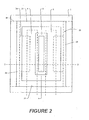
- Figure 2 depicts a similar transistor structure as shown in figure 1. This figure only shows the drain region and indicates the, sinker, the source region, and the gates by broken lines. Similar structures and elements carry similar numerals.
- an additional p doped ring structure 20 is implanted that extends from the surface of the active area 1 into the epitaxial layer to additionally isolate transistor structures as will be shown in more detail in Fig. 3.
- Figure 2 shows the p doped ring as rectangular ring structure with two parallel "vertical" areas 22 and two parallel “horizontal” areas 21.
- other forms, such as a circle, oval, hexagonal, or any other polygon shape can be used.
- the such formed inter-unit cell p ring 20 completely surrounds both transistors.
- the p ring profile can be generated by masked ion implant, for example, with a boron dose in the range of 10 14 -10 15 /cm 2 .
- the inter-unit cells p ring thus, is created with a lower dose than the p + sinker and is used to terminate the electrical field (depletion region) at the end of the unit cells to prevent the electrical field to come in contact with the defect centers, thus limiting the leakage current and providing the leakage current insulating function.
- the lower dose p ring design reduces the implant damage, improves the source resistance, and suppresses the snapback behavior
- the depletion edge extends along the end of the drain fingers 8, 9 with increasing drain bias.
- a drain to source leakage path can be formed when the depletion region, in case of an electrical field>0, starts covering the stress and implant damage induced defect centers.
- the inter-unit cells p ring terminates the electrical field (depletion region) at the end of unit cells and effectively prevents the electrical field to come in contact with the defect centers and, thus, suppress the leakage current.
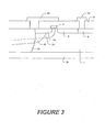
- Figure 3 shows the P ring profile within the transistor structure in a sectional view along the line 3-3 of figure 2.
- a wafer comprises for example an active p-area created by the LOCOS process which includes n-type areas 8, 9 and 34 implanted on the surface to provide a drain and source region, respectively.
- the backside of the substrate comprises a wafer backside metal layer 30 which can be made of gold or aluminum and is used for contact purposes.
- the area 1 is usually covered with an insulator layer 31 such as silicon oxide in which a polysilicium gate 4 is arranged to cover the channel between the drain region 8 and source region 34.
- a passivation layer (not indicated in Fig.
- the source 34 in this exemplary LDMOS transistor can be additionally surrounded by a p doped well 35 depending on what type of technology is used. Electrodes 33 and 32 made of gold or aluminum or any other suitable metal reach through the insulating layer 31 to provide respective couplings between runners for the drain and the source regions, respectively. Runners can also be contacted with the respective drain, source and gate regions by other suitable means, such as, vias or similar coupling structures. To generally reduce a feedback capacitance, the source runner 33 is here extended to cover the gate 4 as shown in Fig. 3. Such a so called field plate over the gate 4 effectively decouples the gate drain capacitance C gd between the gate and the drain. However, other embodiments for the runners are possible.
- a p + sinker implant 36 similar as used in the prior art embodiment of figure 1 is shown on the left side of the source 34 of the left transistor.
- a p + sinker 36 can be created by ion implantation. Effectively, this p + sinker merges with the p well area 35 and, thus, reaches from the source runner contact 33 to the backside metal layer 30.
- the p ring 20 surrounds or encloses the transistor structure. As shown in Figure 3, the p ring structure extends from the surface of the active area 1 downwards. Furthermore, the p ring 20 partially overlaps with the p + sinker and the source region 34 in areas 22 (see Fig. 2) where the source 34 and the p + sinker 36 are located.
- these areas 22 extend along the left and the right side of the drain regions 8, 9.
- the p ring 20 in Fig. 3 reaches from the surface into the active area in the areas 21 and 22 (as shown in Fig. 2) and encloses the combined transistor.
- the p + sinker 36 can reach over the boundaries of the active area 1.
- the p ring 20 is completely located within the active area 1.
- the p ring 20 can reach the right and left sides of the field oxide. (LOCOS edge). If no sinker structure is present, this can be done by designing the ring to extend from the left and right side into the active area. However, as shown in Fig. 2, if a p + sinker is used it will merge with the p ring 20 and thus, p ring 20 can extend to the edge of the field oxide.
- the embodiment shown describes a combined dual transistor arrangement.
- the principle of an insulating ring according to the present application can also be applied to structures with more than two transistors or to a single transistor structure.
- the substrate/epitaxial layer can be a p-type or an n-type substrate.
- source, drain region, the p ring, and other doped areas would be according to their function either of the n-type or the p-type.
- the ring structure does not have to be in a rectangular form as shown in figure 2.
- other suitable surrounding shapes can be used, such as a circle, oval, hexagonal, or any other polygon shape.
- Figure 4 A-F shows an exemplary variety of different ring shapes.
- Fig. 4A depicts a circle shape
- Fig. 4B a polygon shape
- Fig. 4D an oval shape.
- the main function is to insulate the electrical field. Therefore, depending on the structure of the transistor the ring might have some openings as long as they do not influence the substantially the shielding function.
- Fig. 4C shows another rectangular or square shape formed by four elements 40.
- Fig. 4F shows another example, of a four element structure 42 with gaps at less critical areas of the ring.
- Fig. 4E only two elements 41 are provided in the "horizontal" areas. These elements 41 merge with the p + sinker structures and, thus, form the insulating ring. Any other ring structure or combination of elements is possible to reach a similar result.
Landscapes
- Insulated Gate Type Field-Effect Transistor (AREA)
Abstract
Description
- The present application relates to an LDMOS transistor structure.
- LDMOS transistor structures are widely used in semiconductor devices for many types of transistor applications such as high voltage MOS field effect transistors. An LDMOS transistor comprises a lightly doped drain region to enhance the breakdown voltage. Fig. 1 shows a top view of a combined transistor structure including two MOSFET transistors. Both transistors are arranged within an active, for example, p doped
area 1 that is isolated from the surroundings, by a so-calledfield region 11. The transistors share a common drain region consisting of a n+ doped region 9 surrounded by a n-doped region 8. Twosource regions 6, 7 are arranged on the left and the right side of thisdrain region 8, 9. Thus, two channels are defined by thedrain region 8, 9 and the twosource regions 6 and 7, respectively. The broken lines indicate thegates source regions 6 and 7, there are arranged p+ sinker structures 2 and 3 which extend from the surface of epitaxial layer to the bottom of the substrate to provide for a source connection on the backside of the substrate. - The
active region 1 can be enclosed by a single step, the LOCal Oxidation of Silicon (LOCOS) as known in the art. - This process creates a so called high stress field oxide bird's beak region which in combination with the p+
sinker structure implants arrows 10. - The conventional solution to prevent such a leakage is to increase the spacing between p+ and n+ implants to the bird's beak to suppress the leakage current. The disadvantages of such a measurement is, however, the increase of the non-functional part of the transistor fingers and the reduction of the isolation region.
- According to the present application, a new transistor structure is introduced which avoids such a leakage.
- A semiconductor device comprises an active region of a first conducting type including a transistor structure, and a ring shaped region of the first conducting type extending from a surface of the active region into the active region and substantially surrounding the transistor structure.
- The transistor structure may comprise, a drain region, a source region, wherein the drain and the source define a channel, a gate being arranged above said channel, and a sinker structure of said first conducting type arranged substantially along said source region reaching from the surface of the active area next to the source region to the bottom of the active area. The p ring can be less doped than the sinker structure. The device may further comprise a metal layer on the backside of the semiconductor device. The transistor structure can be a two transistor structure comprising, a common drain region, a first source region arranged on one side of the common drain region, a second source region arranged on the respective opposite side of the drain region, wherein the drain region and the source regions each define a channel, a first and second gate being arranged above said channels, and a first and second sinker structure of said first conducting type arranged substantially along said source regions reaching from the surface of the active area next to the respective source regions to the bottom of the active area. The drain region may comprise a lightly doped drain region. The ring can be doped in the range of 1014-1015/cm2. The active area can be created and enclosed by a LOCOS process. The active area may comprise a substrate and an epitaxial layer on top of said substrate. The first conducting type can be the p type or n type. The ring can be created by masked ion implant. Boron can be used as a dopant. The ring may have a rectangular, circular, oval, or polygon shape. The ring may comprise at least one gap that does not substantially influence an insulating function of the ring.
- According to another embodiment, a semiconductor device comprises an active region of a first conducting type including a transistor structure, wherein the transistor structure comprises, a drain region of a second type, a channel, and a gate being arranged above said channel, and a ring shaped region of the first conducting type extending from a surface of the active region into the active region and surrounding the transistor structure.
- The device may further comprise a source region of the second type arranged along one side of the drain region, and a sinker structure of said first conducting type arranged substantially along said source region reaching from the surface of the active area next to the source region to the bottom of the active area. The device can also further comprise a second source region arranged on the respective opposite side of the drain region, wherein the drain region and the source regions each define a channel, a first and second gate being arranged above said channels, and a first and second sinker structure of said first conducting type arranged substantially along said source regions reaching from the surface of the active area next to the respective source regions to the bottom of the active area. Again, the drain region may comprise a lightly doped drain region and the device may further comprise a metal layer on the backside of the semiconductor device. The ring may be less doped than the sinker structure and can be doped in the range of 1014-1015/cm2. The active area can be created and enclosed by a LOCOS process. The active area may comprise a substrate and an epitaxial layer on top of said substrate. The first conducting type can be the p type or n-type. The ring can be created by masked ion implant. Boron can be used as a dopant. The ring may have a rectangular, circular, oval, polygon, or partially open shape. The ring may further comprise at least one gap that does not substantially influence an insulating function of the ring.
- A method of manufacturing a semiconductor device comprises the steps of:
- forming an active region of a first conducting type within a semiconductor material;
- forming a transistor structure, and
- forming a ring shaped region of the first conducting type extending from a surface of the active region into the active region and surrounding the transistor structure.
- The step of forming a transistor structure may comprise the steps of forming a drain region of a second type, a source region of the second type arranged along one side of the drain region, and a sinker structure of said first conducting type arranged substantially along said source region reaching from the surface of the active area next to the source region to the bottom of the active area. The method may further comprise the step of forming a second source region arranged on the respective opposite side of the drain region, and a first and second sinker structure of said first conducting type arranged substantially along said source regions reaching from the surface of the active area next to the respective source regions to the bottom of the active area. The drain region can be formed in such a way that it comprises a lightly doped drain region. The method may further comprise the step of arranging a metal layer on the backside of the semiconductor device. The step of forming the ring may include the step of doping the ring less than the sinker structure. The ring can be doped in the range of 1014-1015/cm2. The active area can be created and enclosed by a LOCOS process. The ring can be created by masked ion implant. Boron may be used as a dopant. The ring can have a rectangular, circular, oval, polygon, or partially open shape.
- Other technical advantages of the present disclosure will be readily apparent to one skilled in the art from the following figures, descriptions, and claims.
- A more complete understanding of the present disclosure and advantages thereof may be acquired by referring to the following description taken in conjunction with the accompanying drawings, in which like reference numbers indicate like features, and wherein:
- Figure 1
- is a top view of a combined transistor structure enclosed by a LOCOS area according to the prior art;
- Figure 2
- is a top view of a combined transistor structure enclosed by a LOCOS area according to an embodiment of the present invention;
- Figure 3
- is a sectional view along the line 3-3 in figure 2.; and
- Figure 4
- shows different possible shapes of the inter unit cell ring.
- Turning to the drawings, an exemplary embodiment of the present application will now be described. Figure 2 depicts a similar transistor structure as shown in figure 1. This figure only shows the drain region and indicates the, sinker, the source region, and the gates by broken lines. Similar structures and elements carry similar numerals. Within the
active area 1, an additional p dopedring structure 20 is implanted that extends from the surface of theactive area 1 into the epitaxial layer to additionally isolate transistor structures as will be shown in more detail in Fig. 3. Figure 2 shows the p doped ring as rectangular ring structure with two parallel "vertical"areas 22 and two parallel "horizontal"areas 21. However, other forms, such as a circle, oval, hexagonal, or any other polygon shape can be used. The such formed inter-unitcell p ring 20 completely surrounds both transistors. The p ring profile can be generated by masked ion implant, for example, with a boron dose in the range of 1014-1015/cm2. The inter-unit cells p ring, thus, is created with a lower dose than the p+ sinker and is used to terminate the electrical field (depletion region) at the end of the unit cells to prevent the electrical field to come in contact with the defect centers, thus limiting the leakage current and providing the leakage current insulating function. The lower dose p ring design reduces the implant damage, improves the source resistance, and suppresses the snapback behavior - For a conventional device, the depletion edge extends along the end of the
drain fingers 8, 9 with increasing drain bias. A drain to source leakage path can be formed when the depletion region, in case of an electrical field>0, starts covering the stress and implant damage induced defect centers.
As stated above, the inter-unit cells p ring terminates the electrical field (depletion region) at the end of unit cells and effectively prevents the electrical field to come in contact with the defect centers and, thus, suppress the leakage current. - Figure 3 shows the P ring profile within the transistor structure in a sectional view along the line 3-3 of figure 2. However, only a partial view is presented and, thus, only the left transistor is shown in this figure. A wafer comprises for example an active p-area created by the LOCOS process which includes n-
type areas backside metal layer 30 which can be made of gold or aluminum and is used for contact purposes. Thearea 1 is usually covered with aninsulator layer 31 such as silicon oxide in which apolysilicium gate 4 is arranged to cover the channel between thedrain region 8 andsource region 34. On top of this layer is usually a passivation layer (not indicated in Fig. 3). Thesource 34 in this exemplary LDMOS transistor can be additionally surrounded by a p doped well 35 depending on what type of technology is used.Electrodes layer 31 to provide respective couplings between runners for the drain and the source regions, respectively. Runners can also be contacted with the respective drain, source and gate regions by other suitable means, such as, vias or similar coupling structures. To generally reduce a feedback capacitance, thesource runner 33 is here extended to cover thegate 4 as shown in Fig. 3. Such a so called field plate over thegate 4 effectively decouples the gate drain capacitance Cgd between the gate and the drain. However, other embodiments for the runners are possible. A p+ sinker implant 36 similar as used in the prior art embodiment of figure 1 is shown on the left side of thesource 34 of the left transistor. Such a p+ sinker 36 can be created by ion implantation. Effectively, this p+ sinker merges with thep well area 35 and, thus, reaches from thesource runner contact 33 to thebackside metal layer 30. Contrary to the p+ sinker 36, thep ring 20 surrounds or encloses the transistor structure. As shown in Figure 3, the p ring structure extends from the surface of theactive area 1 downwards. Furthermore, thep ring 20 partially overlaps with the p+ sinker and thesource region 34 in areas 22 (see Fig. 2) where thesource 34 and the p+ sinker 36 are located. As indicated in figure 2, theseareas 22 extend along the left and the right side of thedrain regions 8, 9. Thus, thep ring 20 in Fig. 3 reaches from the surface into the active area in theareas 21 and 22 (as shown in Fig. 2) and encloses the combined transistor. Again, the p+ sinker 36 can reach over the boundaries of theactive area 1. However, thep ring 20 is completely located within theactive area 1. As also indicated in Fig. 2, thep ring 20 can reach the right and left sides of the field oxide. (LOCOS edge). If no sinker structure is present, this can be done by designing the ring to extend from the left and right side into the active area. However, as shown in Fig. 2, if a p+ sinker is used it will merge with thep ring 20 and thus,p ring 20 can extend to the edge of the field oxide. - Although particular embodiments of the invention have been shown and described, the invention is not limited to the preferred embodiments and it will be apparent to those skilled in the art that various changes and modifications may be made without departing from the scope of the invention, which is defined only by the appended claims and their equivalents. For example, the embodiment shown describes a combined dual transistor arrangement. However, the principle of an insulating ring according to the present application can also be applied to structures with more than two transistors or to a single transistor structure. Furthermore, the substrate/epitaxial layer can be a p-type or an n-type substrate. Thus, source, drain region, the p ring, and other doped areas would be according to their function either of the n-type or the p-type.
- Furthermore, the ring structure does not have to be in a rectangular form as shown in figure 2. Depending on the form of the transistor structure other suitable surrounding shapes can be used, such as a circle, oval, hexagonal, or any other polygon shape. Figure 4 A-F shows an exemplary variety of different ring shapes. For example, Fig. 4A depicts a circle shape, Fig. 4B a polygon shape, and Fig. 4D an oval shape. The main function is to insulate the electrical field. Therefore, depending on the structure of the transistor the ring might have some openings as long as they do not influence the substantially the shielding function. Fig. 4C, thus, shows another rectangular or square shape formed by four
elements 40. Theseelements 40 can merge at their respective ends to form a continuous rectangular ring structure but also could have small gaps as long as the insulating function is kept. Fig. 4F shows another example, of a fourelement structure 42 with gaps at less critical areas of the ring. In Fig. 4E only twoelements 41 are provided in the "horizontal" areas. Theseelements 41 merge with the p+ sinker structures and, thus, form the insulating ring. Any other ring structure or combination of elements is possible to reach a similar result.
Claims (42)
- A semiconductor device comprising:an active region of a first conducting type including a transistor structure,a ring shaped region of the first conducting type extending from a surface of the active region into the active region and substantially surrounding the transistor structure.
- The device as in claim 1, wherein the transistor structure comprises, a drain region, a source region, wherein the drain and the source define a channel, a gate being arranged above said channel, and a sinker structure of said first conducting type arranged substantially along said source region reaching from the surface of the active area next to the source region to the bottom of the active area.
- The device as in claim 2, wherein the p ring is less doped than the sinker structure.
- The device as in claim 2, wherein the drain region comprises a lightly doped drain region.
- The device as in claim 4, further comprising a metal layer on the backside of the semiconductor device.
- The device as in claim 1, wherein the transistor structure is a two transistor structure comprising, a common drain region, a first source region arranged on one side of the common drain region, a second source region arranged on the respective opposite side of the drain region, wherein the drain region and the source regions each define a channel, a first and second gate being arranged above said channels, and a first and second sinker structure of said first conducting type arranged substantially along said source regions reaching from the surface of the active area next to the respective source regions to the bottom of the active area.
- The device as in claim 5, wherein the drain region comprises a lightly doped drain region.
- The device as in claim 5, further comprising a metal layer on the backside of the semiconductor device.
- The device as in claim 5, wherein the ring is less doped than the sinker structure.
- The device as in claim 1, wherein the ring is doped in the range of 1014-1015/cm2.
- The device as in claim 1, wherein the active area is created and enclosed by a LOCOS process.
- The device as in claim 11, wherein the active area comprises a substrate and an epitaxial layer on top of said substrate.
- The device as in claim 1, wherein the first conducting type is the p type.
- The device as in claim 1, wherein the ring is created by masked ion implant.
- The device as in claim 10 wherein boron is used as a dopant.
- The device as in claim 1, wherein the ring has rectangular, circular, oval, or polygon shape.
- The device as in claim 1, wherein the ring comprises at least one gap that does not substantially influence an insulating function of the ring.
- A semiconductor device comprising:an active region of a first conducting type including a transistor structure, wherein the transistor structure comprises, a drain region of a second type, a channel, and a gate being arranged above said channel, anda ring shaped region of the first conducting type extending from a surface of the active region into the active region and surrounding the transistor structure.
- The device as in claim 18, further comprising a source region of the second type arranged along one side of the drain region, and a sinker structure of said first conducting type arranged substantially along said source region reaching from the surface of the active area next to the source region to the bottom of the active area.
- The device as in claim 19, further comprising a second source region arranged on the respective opposite side of the drain region, wherein the drain region and the source regions each define a channel, a first and second gate being arranged above said channels, and a first and second sinker structure of said first conducting type arranged substantially along said source regions reaching from the surface of the active area next to the respective source regions to the bottom of the active area.
- The device as in claim 18, wherein the drain region comprises a lightly doped drain region.
- The device as in claim 19, further comprising a metal layer on the backside of the semiconductor device.
- The device as in claim 19, wherein the ring is less doped than the sinker structure.
- The device as in claim 18, wherein the ring is doped in the range of 1014-1015/cm2.
- The device as in claim 18, wherein the active area is created and enclosed by a LOCOS process.
- The device as in claim 25, wherein the active area comprises a substrate and an epitaxial layer on top of said substrate.
- The device as in claim 18, wherein the first conducting type is the p type.
- The device as in claim 18, wherein the ring is created by masked ion implant.
- The device as in claim 24, wherein boron is used as a dopant.
- The device as in claim 18, wherein the ring has a rectangular, circular, oval, polygon, or partially open shape.
- The device as in claim 18, wherein the ring comprises at least one gap that does not substantially influence an insulating function of the ring.
- A method of manufacturing a semiconductor device comprising the steps of:forming an active region of a first conducting type within a semiconductor material;forming a transistor structure, andforming a ring shaped region of the first conducting type extending from a surface of the active region into the active region and surrounding the transistor structure.
- The method as in claim 32, wherein the step of forming a transistor structure comprises the steps of forming a drain region of a second type, a source region of the second type arranged along one side of the drain region, and a sinker structure of said first conducting type arranged substantially along said source region reaching from the surface of the active area next to the source region to the bottom of the active area.
- The method as in claim 33, further comprising the step of forming a second source region arranged on the respective opposite side of the drain region, and a first and second sinker structure of said first conducting type arranged substantially along said source regions reaching from the surface of the active area next to the respective source regions to the bottom of the active area.
- The method as in claim 32, wherein the drain region is formed in such a way that it comprises a lightly doped drain region.
- The method as in claim 33, further comprising the step of arranging a metal layer on the backside of the semiconductor device.
- The device as in claim 32, wherein the step of forming the ring includes the step of doping the ring less than the sinker structure.
- The method as in claim 32, wherein the ring is doped in the range of 1014-1015/cm2.
- The method as in claim 32, wherein the active area is created and enclosed by a LOCOS process.
- The method as in claim 32, wherein the ring is created by masked ion implant.
- The method as in claim 32, wherein boron is used as a dopant.
- The method as in claim 32, wherein the ring has a rectangular, circular, oval, polygon, or partially open shape.
Applications Claiming Priority (2)
| Application Number | Priority Date | Filing Date | Title |
|---|---|---|---|
| US663051 | 1984-10-19 | ||
| US10/663,051 US7049669B2 (en) | 2003-09-15 | 2003-09-15 | LDMOS transistor |
Publications (3)
| Publication Number | Publication Date |
|---|---|
| EP1515371A2 true EP1515371A2 (en) | 2005-03-16 |
| EP1515371A3 EP1515371A3 (en) | 2008-03-26 |
| EP1515371B1 EP1515371B1 (en) | 2015-04-29 |
Family
ID=34136819
Family Applications (1)
| Application Number | Title | Priority Date | Filing Date |
|---|---|---|---|
| EP20040021508 Expired - Lifetime EP1515371B1 (en) | 2003-09-15 | 2004-09-09 | Semiconductor device comprising a MOS transistor and method of making the same |
Country Status (3)
| Country | Link |
|---|---|
| US (1) | US7049669B2 (en) |
| EP (1) | EP1515371B1 (en) |
| JP (1) | JP2005123593A (en) |
Families Citing this family (18)
| Publication number | Priority date | Publication date | Assignee | Title |
|---|---|---|---|---|
| US20060071304A1 (en) | 2004-09-29 | 2006-04-06 | International Business Machines Corporation | Structure and layout of a fet prime cell |
| US20080291973A1 (en) * | 2004-11-16 | 2008-11-27 | Acco | Integrated Ultra-Wideband (Uwb) Pulse Generator |
| US7518218B2 (en) * | 2005-03-03 | 2009-04-14 | Aeroflex Colorado Springs, Inc. | Total ionizing dose suppression transistor architecture |
| EP1935026A1 (en) | 2005-10-12 | 2008-06-25 | Acco | Insulated gate field-effet transistor having a dummy gate |
| US7969243B2 (en) | 2009-04-22 | 2011-06-28 | Acco Semiconductor, Inc. | Electronic circuits including a MOSFET and a dual-gate JFET |
| US7863645B2 (en) * | 2008-02-13 | 2011-01-04 | ACCO Semiconductor Inc. | High breakdown voltage double-gate semiconductor device |
| US8928410B2 (en) | 2008-02-13 | 2015-01-06 | Acco Semiconductor, Inc. | Electronic circuits including a MOSFET and a dual-gate JFET |
| US9240402B2 (en) | 2008-02-13 | 2016-01-19 | Acco Semiconductor, Inc. | Electronic circuits including a MOSFET and a dual-gate JFET |
| US7808415B1 (en) * | 2009-03-25 | 2010-10-05 | Acco Semiconductor, Inc. | Sigma-delta modulator including truncation and applications thereof |
| US7952431B2 (en) * | 2009-08-28 | 2011-05-31 | Acco Semiconductor, Inc. | Linearization circuits and methods for power amplification |
| TWI497691B (en) * | 2009-09-09 | 2015-08-21 | United Microelectronics Corp | Ultra high voltage mos tarnsistor device |
| US8115253B2 (en) * | 2009-09-10 | 2012-02-14 | United Microelectronics Corp. | Ultra high voltage MOS transistor device |
| US8532584B2 (en) | 2010-04-30 | 2013-09-10 | Acco Semiconductor, Inc. | RF switches |
| JP2011249728A (en) * | 2010-05-31 | 2011-12-08 | Toshiba Corp | Semiconductor device and method for manufacturing the same |
| CN102361035A (en) * | 2011-10-21 | 2012-02-22 | 昆山华太电子技术有限公司 | Structure of RF-LDMOS (radio frequency laterally double-diffused metal oxide semiconductor) device without epitaxial layer |
| CN103091533B (en) * | 2011-11-03 | 2014-12-10 | 上海华虹宏力半导体制造有限公司 | Current sampling circuit achieved by laterally diffused metal oxide semiconductor (LDMOS) devices |
| US11171215B2 (en) | 2014-12-18 | 2021-11-09 | Silanna Asia Pte Ltd | Threshold voltage adjustment using adaptively biased shield plate |
| US9559199B2 (en) | 2014-12-18 | 2017-01-31 | Silanna Asia Pte Ltd | LDMOS with adaptively biased gate-shield |
Citations (3)
| Publication number | Priority date | Publication date | Assignee | Title |
|---|---|---|---|---|
| WO2000008674A2 (en) | 1998-08-05 | 2000-02-17 | Spectrian, Inc. | Mosfet having self-aligned gate and buried shield and method of making same |
| US6222233B1 (en) | 1999-10-04 | 2001-04-24 | Xemod, Inc. | Lateral RF MOS device with improved drain structure |
| US20010012671A1 (en) | 1999-09-21 | 2001-08-09 | Yutaka Hoshino | Semiconductor device and a method of manufacturing the same |
Family Cites Families (36)
| Publication number | Priority date | Publication date | Assignee | Title |
|---|---|---|---|---|
| JPS5286083A (en) * | 1976-01-12 | 1977-07-16 | Hitachi Ltd | Production of complimentary isolation gate field effect transistor |
| US4013484A (en) * | 1976-02-25 | 1977-03-22 | Intel Corporation | High density CMOS process |
| IT1210872B (en) * | 1982-04-08 | 1989-09-29 | Ates Componenti Elettron | PROCESS FOR THE MANUFACTURE OF COMPLEMENTARY MOS TRANSISTORS IN HIGH DENSITY INTEGRATED CIRCUITS FOR HIGH VOLTAGES. |
| US4811075A (en) * | 1987-04-24 | 1989-03-07 | Power Integrations, Inc. | High voltage MOS transistors |
| US5026656A (en) * | 1988-02-01 | 1991-06-25 | Texas Instruments Incorporated | MOS transistor with improved radiation hardness |
| US5192993A (en) * | 1988-09-27 | 1993-03-09 | Kabushiki Kaisha Toshiba | Semiconductor device having improved element isolation area |
| US5156989A (en) * | 1988-11-08 | 1992-10-20 | Siliconix, Incorporated | Complementary, isolated DMOS IC technology |
| US5155563A (en) * | 1991-03-18 | 1992-10-13 | Motorola, Inc. | Semiconductor device having low source inductance |
| US5386136A (en) * | 1991-05-06 | 1995-01-31 | Siliconix Incorporated | Lightly-doped drain MOSFET with improved breakdown characteristics |
| US5374843A (en) * | 1991-05-06 | 1994-12-20 | Silinconix, Inc. | Lightly-doped drain MOSFET with improved breakdown characteristics |
| US5252848A (en) * | 1992-02-03 | 1993-10-12 | Motorola, Inc. | Low on resistance field effect transistor |
| US5313082A (en) * | 1993-02-16 | 1994-05-17 | Power Integrations, Inc. | High voltage MOS transistor with a low on-resistance |
| US5578860A (en) * | 1995-05-01 | 1996-11-26 | Motorola, Inc. | Monolithic high frequency integrated circuit structure having a grounded source configuration |
| EP0762493A1 (en) * | 1995-08-03 | 1997-03-12 | Motorola, Inc. | Semiconductor device having field oxide regions and a field implant and method of manufacturing the same |
| US5723985A (en) * | 1995-11-21 | 1998-03-03 | Information Storage Devices, Inc. | Clocked high voltage switch |
| US5801418A (en) * | 1996-02-12 | 1998-09-01 | International Rectifier Corporation | High voltage power integrated circuit with level shift operation and without metal crossover |
| US5747853A (en) * | 1996-08-07 | 1998-05-05 | Megamos Corporation | Semiconductor structure with controlled breakdown protection |
| US6168983B1 (en) * | 1996-11-05 | 2001-01-02 | Power Integrations, Inc. | Method of making a high-voltage transistor with multiple lateral conduction layers |
| US5844276A (en) * | 1996-12-06 | 1998-12-01 | Advanced Micro Devices, Inc. | CMOS integrated circuit and method for implanting NMOS transistor areas prior to implanting PMOS transistor areas to optimize the thermal diffusivity thereof |
| US6297533B1 (en) * | 1997-12-04 | 2001-10-02 | The Whitaker Corporation | LDMOS structure with via grounded source |
| US5949104A (en) * | 1998-02-07 | 1999-09-07 | Xemod, Inc. | Source connection structure for lateral RF MOS devices |
| US5900663A (en) * | 1998-02-07 | 1999-05-04 | Xemod, Inc. | Quasi-mesh gate structure for lateral RF MOS devices |
| US6001710A (en) * | 1998-03-30 | 1999-12-14 | Spectrian, Inc. | MOSFET device having recessed gate-drain shield and method |
| JP2000031265A (en) * | 1998-07-14 | 2000-01-28 | Nec Corp | Method for manufacturing semiconductor device |
| US6448160B1 (en) * | 1999-04-01 | 2002-09-10 | Apd Semiconductor, Inc. | Method of fabricating power rectifier device to vary operating parameters and resulting device |
| US6624030B2 (en) * | 2000-12-19 | 2003-09-23 | Advanced Power Devices, Inc. | Method of fabricating power rectifier device having a laterally graded P-N junction for a channel region |
| JP3942324B2 (en) * | 1999-09-29 | 2007-07-11 | Necエレクトロニクス株式会社 | Input protection circuit |
| US6372557B1 (en) * | 2000-04-19 | 2002-04-16 | Polyfet Rf Devices, Inc. | Method of manufacturing a lateral fet having source contact to substrate with low resistance |
| JP2001339047A (en) * | 2000-05-29 | 2001-12-07 | Matsushita Electric Ind Co Ltd | Semiconductor device |
| US6355960B1 (en) * | 2000-09-18 | 2002-03-12 | Vanguard International Semiconductor Corporation | ESD protection for open drain I/O pad in integrated circuit with parasitic field FET devices |
| US6825543B2 (en) * | 2000-12-28 | 2004-11-30 | Canon Kabushiki Kaisha | Semiconductor device, method for manufacturing the same, and liquid jet apparatus |
| US6424007B1 (en) * | 2001-01-24 | 2002-07-23 | Power Integrations, Inc. | High-voltage transistor with buried conduction layer |
| JP2002343894A (en) * | 2001-05-16 | 2002-11-29 | Matsushita Electric Ind Co Ltd | Semiconductor device |
| WO2003021684A1 (en) * | 2001-09-04 | 2003-03-13 | Koninklijke Philips Electronics N.V. | Method for producing a semiconductor device having an edge structure |
| KR100431066B1 (en) * | 2001-09-27 | 2004-05-12 | 삼성전자주식회사 | Semiconductor device having electro-static discharge circuit |
| US6710416B1 (en) * | 2003-05-16 | 2004-03-23 | Agere Systems Inc. | Split-gate metal-oxide-semiconductor device |
-
2003
- 2003-09-15 US US10/663,051 patent/US7049669B2/en not_active Expired - Lifetime
-
2004
- 2004-09-09 EP EP20040021508 patent/EP1515371B1/en not_active Expired - Lifetime
- 2004-09-13 JP JP2004264898A patent/JP2005123593A/en active Pending
Patent Citations (3)
| Publication number | Priority date | Publication date | Assignee | Title |
|---|---|---|---|---|
| WO2000008674A2 (en) | 1998-08-05 | 2000-02-17 | Spectrian, Inc. | Mosfet having self-aligned gate and buried shield and method of making same |
| US20010012671A1 (en) | 1999-09-21 | 2001-08-09 | Yutaka Hoshino | Semiconductor device and a method of manufacturing the same |
| US6222233B1 (en) | 1999-10-04 | 2001-04-24 | Xemod, Inc. | Lateral RF MOS device with improved drain structure |
Also Published As
| Publication number | Publication date |
|---|---|
| EP1515371B1 (en) | 2015-04-29 |
| US20050056889A1 (en) | 2005-03-17 |
| JP2005123593A (en) | 2005-05-12 |
| EP1515371A3 (en) | 2008-03-26 |
| US7049669B2 (en) | 2006-05-23 |
Similar Documents
| Publication | Publication Date | Title |
|---|---|---|
| US7049669B2 (en) | LDMOS transistor | |
| US7125777B2 (en) | Asymmetric hetero-doped high-voltage MOSFET (AH2MOS) | |
| US8722477B2 (en) | Cascoded high voltage junction field effect transistor | |
| US8652930B2 (en) | Semiconductor device with self-biased isolation | |
| TWI570914B (en) | Semiconductor device | |
| US9680011B2 (en) | Self-adjusted isolation bias in semiconductor devices | |
| US8026549B2 (en) | LDMOS with N-type isolation ring and method of fabricating the same | |
| US20090206913A1 (en) | Edge Termination with Improved Breakdown Voltage | |
| US20050199952A1 (en) | Termination structure for trench DMOS device and method of making the same | |
| CN101919042A (en) | Semiconductor power module with electrostatic discharge circuit protection capable of reducing mask number | |
| JP2005510881A (en) | Trench metal oxide semiconductor field effect transistor device with improved on-resistance | |
| US10038082B2 (en) | Cascoded high voltage junction field effect transistor | |
| US20090309169A1 (en) | Structure for Preventing Leakage of a Semiconductor Device | |
| US10340147B2 (en) | Semiconductor device with equipotential ring contact at curved portion of equipotential ring electrode and method of manufacturing the same | |
| KR101051684B1 (en) | Electrostatic discharge protection device and manufacturing method | |
| KR100555280B1 (en) | Semiconductor device and manufacturing method thereof | |
| US12557618B2 (en) | Semiconductor device | |
| US9324800B1 (en) | Bidirectional MOSFET with suppressed bipolar snapback and method of manufacture | |
| JP3354127B2 (en) | High voltage element and method of manufacturing the same | |
| US20100224909A1 (en) | Semiconductor device and method for fabricating the same | |
| US7473974B2 (en) | Semiconductor circuit device including a protection circuit | |
| JP4584222B2 (en) | Manufacturing method of high voltage transistor | |
| US20100102379A1 (en) | Lateral diffused metal oxide semiconductor device | |
| US20250142877A1 (en) | Gate trench power semiconductor devices having trench shielding regions and support shields that extend to different depths | |
| JP2004349384A (en) | Semiconductor device |
Legal Events
| Date | Code | Title | Description |
|---|---|---|---|
| PUAI | Public reference made under article 153(3) epc to a published international application that has entered the european phase |
Free format text: ORIGINAL CODE: 0009012 |
|
| AK | Designated contracting states |
Kind code of ref document: A2 Designated state(s): AT BE BG CH CY CZ DE DK EE ES FI FR GB GR HU IE IT LI LU MC NL PL PT RO SE SI SK TR |
|
| AX | Request for extension of the european patent |
Extension state: AL HR LT LV MK |
|
| PUAL | Search report despatched |
Free format text: ORIGINAL CODE: 0009013 |
|
| AK | Designated contracting states |
Kind code of ref document: A3 Designated state(s): AT BE BG CH CY CZ DE DK EE ES FI FR GB GR HU IE IT LI LU MC NL PL PT RO SE SI SK TR |
|
| AX | Request for extension of the european patent |
Extension state: AL HR LT LV MK |
|
| RIC1 | Information provided on ipc code assigned before grant |
Ipc: H01L 29/78 20060101AFI20041222BHEP Ipc: H01L 21/336 20060101ALI20080221BHEP Ipc: H01L 21/762 20060101ALI20080221BHEP Ipc: H01L 29/10 20060101ALI20080221BHEP Ipc: H01L 29/06 20060101ALI20080221BHEP |
|
| 17P | Request for examination filed |
Effective date: 20080910 |
|
| 17Q | First examination report despatched |
Effective date: 20081103 |
|
| AKX | Designation fees paid |
Designated state(s): DE FR GB |
|
| RAP1 | Party data changed (applicant data changed or rights of an application transferred) |
Owner name: INFINEON TECHNOLOGIES AG |
|
| RIC1 | Information provided on ipc code assigned before grant |
Ipc: H01L 21/336 20060101ALI20141023BHEP Ipc: H01L 21/762 20060101ALN20141023BHEP Ipc: H01L 29/78 20060101AFI20141023BHEP Ipc: H01L 29/10 20060101ALI20141023BHEP Ipc: H01L 29/06 20060101ALI20141023BHEP |
|
| GRAP | Despatch of communication of intention to grant a patent |
Free format text: ORIGINAL CODE: EPIDOSNIGR1 |
|
| INTG | Intention to grant announced |
Effective date: 20141223 |
|
| GRAS | Grant fee paid |
Free format text: ORIGINAL CODE: EPIDOSNIGR3 |
|
| GRAA | (expected) grant |
Free format text: ORIGINAL CODE: 0009210 |
|
| AK | Designated contracting states |
Kind code of ref document: B1 Designated state(s): DE FR GB |
|
| REG | Reference to a national code |
Ref country code: GB Ref legal event code: FG4D |
|
| REG | Reference to a national code |
Ref country code: DE Ref legal event code: R096 Ref document number: 602004047089 Country of ref document: DE Effective date: 20150618 |
|
| REG | Reference to a national code |
Ref country code: DE Ref legal event code: R097 Ref document number: 602004047089 Country of ref document: DE |
|
| PLBE | No opposition filed within time limit |
Free format text: ORIGINAL CODE: 0009261 |
|
| STAA | Information on the status of an ep patent application or granted ep patent |
Free format text: STATUS: NO OPPOSITION FILED WITHIN TIME LIMIT |
|
| 26N | No opposition filed |
Effective date: 20160201 |
|
| GBPC | Gb: european patent ceased through non-payment of renewal fee |
Effective date: 20150909 |
|
| REG | Reference to a national code |
Ref country code: FR Ref legal event code: ST Effective date: 20160531 |
|
| PG25 | Lapsed in a contracting state [announced via postgrant information from national office to epo] |
Ref country code: GB Free format text: LAPSE BECAUSE OF NON-PAYMENT OF DUE FEES Effective date: 20150909 |
|
| PG25 | Lapsed in a contracting state [announced via postgrant information from national office to epo] |
Ref country code: FR Free format text: LAPSE BECAUSE OF NON-PAYMENT OF DUE FEES Effective date: 20150930 |
|
| PGFP | Annual fee paid to national office [announced via postgrant information from national office to epo] |
Ref country code: DE Payment date: 20171129 Year of fee payment: 14 |
|
| REG | Reference to a national code |
Ref country code: DE Ref legal event code: R119 Ref document number: 602004047089 Country of ref document: DE |
|
| PG25 | Lapsed in a contracting state [announced via postgrant information from national office to epo] |
Ref country code: DE Free format text: LAPSE BECAUSE OF NON-PAYMENT OF DUE FEES Effective date: 20190402 |