EP1515369B1 - Light-emitting device substrate and light-emitting device using the same - Google Patents
Light-emitting device substrate and light-emitting device using the same Download PDFInfo
- Publication number
- EP1515369B1 EP1515369B1 EP04090343A EP04090343A EP1515369B1 EP 1515369 B1 EP1515369 B1 EP 1515369B1 EP 04090343 A EP04090343 A EP 04090343A EP 04090343 A EP04090343 A EP 04090343A EP 1515369 B1 EP1515369 B1 EP 1515369B1
- Authority
- EP
- European Patent Office
- Prior art keywords
- layer
- light
- refractive index
- emitting device
- substrate
- Prior art date
- Legal status (The legal status is an assumption and is not a legal conclusion. Google has not performed a legal analysis and makes no representation as to the accuracy of the status listed.)
- Expired - Lifetime
Links
- 239000000758 substrate Substances 0.000 title claims description 154
- 230000003287 optical effect Effects 0.000 claims description 14
- 238000009826 distribution Methods 0.000 claims description 5
- 239000010410 layer Substances 0.000 description 347
- 238000000605 extraction Methods 0.000 description 34
- 238000000034 method Methods 0.000 description 33
- GWEVSGVZZGPLCZ-UHFFFAOYSA-N Titan oxide Chemical compound O=[Ti]=O GWEVSGVZZGPLCZ-UHFFFAOYSA-N 0.000 description 28
- 230000000052 comparative effect Effects 0.000 description 23
- 239000000463 material Substances 0.000 description 23
- VYPSYNLAJGMNEJ-UHFFFAOYSA-N Silicium dioxide Chemical compound O=[Si]=O VYPSYNLAJGMNEJ-UHFFFAOYSA-N 0.000 description 22
- 230000003667 anti-reflective effect Effects 0.000 description 20
- 238000000151 deposition Methods 0.000 description 11
- 230000008021 deposition Effects 0.000 description 11
- 238000005229 chemical vapour deposition Methods 0.000 description 10
- 238000004519 manufacturing process Methods 0.000 description 10
- 238000004544 sputter deposition Methods 0.000 description 10
- 229910052681 coesite Inorganic materials 0.000 description 9
- 229910052906 cristobalite Inorganic materials 0.000 description 9
- 239000000377 silicon dioxide Substances 0.000 description 9
- 229910052682 stishovite Inorganic materials 0.000 description 9
- 229910052905 tridymite Inorganic materials 0.000 description 9
- 238000006243 chemical reaction Methods 0.000 description 8
- 239000011521 glass Substances 0.000 description 8
- 229910010272 inorganic material Inorganic materials 0.000 description 8
- 239000011147 inorganic material Substances 0.000 description 8
- 239000011368 organic material Substances 0.000 description 7
- -1 quinolinol metal complex Chemical class 0.000 description 6
- 230000000694 effects Effects 0.000 description 5
- 239000010408 film Substances 0.000 description 5
- 239000010409 thin film Substances 0.000 description 5
- MCMNRKCIXSYSNV-UHFFFAOYSA-N Zirconium dioxide Chemical compound O=[Zr]=O MCMNRKCIXSYSNV-UHFFFAOYSA-N 0.000 description 4
- 239000002131 composite material Substances 0.000 description 4
- 238000010438 heat treatment Methods 0.000 description 4
- 238000001659 ion-beam spectroscopy Methods 0.000 description 4
- ZKATWMILCYLAPD-UHFFFAOYSA-N niobium pentoxide Chemical compound O=[Nb](=O)O[Nb](=O)=O ZKATWMILCYLAPD-UHFFFAOYSA-N 0.000 description 4
- 238000002294 plasma sputter deposition Methods 0.000 description 4
- 238000001771 vacuum deposition Methods 0.000 description 4
- 229910052782 aluminium Inorganic materials 0.000 description 3
- XAGFODPZIPBFFR-UHFFFAOYSA-N aluminium Chemical compound [Al] XAGFODPZIPBFFR-UHFFFAOYSA-N 0.000 description 3
- 230000001419 dependent effect Effects 0.000 description 3
- 238000004020 luminiscence type Methods 0.000 description 3
- 238000005215 recombination Methods 0.000 description 3
- 230000006798 recombination Effects 0.000 description 3
- 238000003980 solgel method Methods 0.000 description 3
- 229910001316 Ag alloy Inorganic materials 0.000 description 2
- UFWIBTONFRDIAS-UHFFFAOYSA-N Naphthalene Chemical compound C1=CC=CC2=CC=CC=C21 UFWIBTONFRDIAS-UHFFFAOYSA-N 0.000 description 2
- 239000004642 Polyimide Substances 0.000 description 2
- 229910004205 SiNX Inorganic materials 0.000 description 2
- 239000004965 Silica aerogel Substances 0.000 description 2
- CDBYLPFSWZWCQE-UHFFFAOYSA-L Sodium Carbonate Chemical compound [Na+].[Na+].[O-]C([O-])=O CDBYLPFSWZWCQE-UHFFFAOYSA-L 0.000 description 2
- 239000007983 Tris buffer Substances 0.000 description 2
- PNEYBMLMFCGWSK-UHFFFAOYSA-N aluminium oxide Inorganic materials [O-2].[O-2].[O-2].[Al+3].[Al+3] PNEYBMLMFCGWSK-UHFFFAOYSA-N 0.000 description 2
- CETPSERCERDGAM-UHFFFAOYSA-N ceric oxide Chemical compound O=[Ce]=O CETPSERCERDGAM-UHFFFAOYSA-N 0.000 description 2
- 229910000422 cerium(IV) oxide Inorganic materials 0.000 description 2
- 239000011248 coating agent Substances 0.000 description 2
- 238000000576 coating method Methods 0.000 description 2
- 239000003086 colorant Substances 0.000 description 2
- 229910052593 corundum Inorganic materials 0.000 description 2
- ZUOUZKKEUPVFJK-UHFFFAOYSA-N diphenyl Chemical compound C1=CC=CC=C1C1=CC=CC=C1 ZUOUZKKEUPVFJK-UHFFFAOYSA-N 0.000 description 2
- 238000010891 electric arc Methods 0.000 description 2
- 238000000313 electron-beam-induced deposition Methods 0.000 description 2
- 230000008020 evaporation Effects 0.000 description 2
- 238000001704 evaporation Methods 0.000 description 2
- 150000002500 ions Chemical class 0.000 description 2
- 238000001182 laser chemical vapour deposition Methods 0.000 description 2
- 239000001989 lithium alloy Substances 0.000 description 2
- CPLXHLVBOLITMK-UHFFFAOYSA-N magnesium oxide Inorganic materials [Mg]=O CPLXHLVBOLITMK-UHFFFAOYSA-N 0.000 description 2
- SJCKRGFTWFGHGZ-UHFFFAOYSA-N magnesium silver Chemical compound [Mg].[Ag] SJCKRGFTWFGHGZ-UHFFFAOYSA-N 0.000 description 2
- 238000001755 magnetron sputter deposition Methods 0.000 description 2
- 239000011159 matrix material Substances 0.000 description 2
- 238000002488 metal-organic chemical vapour deposition Methods 0.000 description 2
- DCZNSJVFOQPSRV-UHFFFAOYSA-N n,n-diphenyl-4-[4-(n-phenylanilino)phenyl]aniline Chemical compound C1=CC=CC=C1N(C=1C=CC(=CC=1)C=1C=CC(=CC=1)N(C=1C=CC=CC=1)C=1C=CC=CC=1)C1=CC=CC=C1 DCZNSJVFOQPSRV-UHFFFAOYSA-N 0.000 description 2
- 238000005240 physical vapour deposition Methods 0.000 description 2
- 238000000623 plasma-assisted chemical vapour deposition Methods 0.000 description 2
- 238000004157 plasmatron Methods 0.000 description 2
- 239000004033 plastic Substances 0.000 description 2
- 229920003023 plastic Polymers 0.000 description 2
- BASFCYQUMIYNBI-UHFFFAOYSA-N platinum Chemical compound [Pt] BASFCYQUMIYNBI-UHFFFAOYSA-N 0.000 description 2
- 229920000139 polyethylene terephthalate Polymers 0.000 description 2
- 229920001721 polyimide Polymers 0.000 description 2
- 229920002635 polyurethane Polymers 0.000 description 2
- 239000004814 polyurethane Substances 0.000 description 2
- 239000010453 quartz Substances 0.000 description 2
- 238000001552 radio frequency sputter deposition Methods 0.000 description 2
- 238000011160 research Methods 0.000 description 2
- PBCFLUZVCVVTBY-UHFFFAOYSA-N tantalum pentoxide Inorganic materials O=[Ta](=O)O[Ta](=O)=O PBCFLUZVCVVTBY-UHFFFAOYSA-N 0.000 description 2
- TVIVIEFSHFOWTE-UHFFFAOYSA-K tri(quinolin-8-yloxy)alumane Chemical compound [Al+3].C1=CN=C2C([O-])=CC=CC2=C1.C1=CN=C2C([O-])=CC=CC2=C1.C1=CN=C2C([O-])=CC=CC2=C1 TVIVIEFSHFOWTE-UHFFFAOYSA-K 0.000 description 2
- 229910001845 yogo sapphire Inorganic materials 0.000 description 2
- RUDFQVOCFDJEEF-UHFFFAOYSA-N yttrium(III) oxide Inorganic materials [O-2].[O-2].[O-2].[Y+3].[Y+3] RUDFQVOCFDJEEF-UHFFFAOYSA-N 0.000 description 2
- QWENRTYMTSOGBR-UHFFFAOYSA-N 1H-1,2,3-Triazole Chemical class C=1C=NNN=1 QWENRTYMTSOGBR-UHFFFAOYSA-N 0.000 description 1
- FQJQNLKWTRGIEB-UHFFFAOYSA-N 2-(4-tert-butylphenyl)-5-[3-[5-(4-tert-butylphenyl)-1,3,4-oxadiazol-2-yl]phenyl]-1,3,4-oxadiazole Chemical compound C1=CC(C(C)(C)C)=CC=C1C1=NN=C(C=2C=C(C=CC=2)C=2OC(=NN=2)C=2C=CC(=CC=2)C(C)(C)C)O1 FQJQNLKWTRGIEB-UHFFFAOYSA-N 0.000 description 1
- OGGKVJMNFFSDEV-UHFFFAOYSA-N 3-methyl-n-[4-[4-(n-(3-methylphenyl)anilino)phenyl]phenyl]-n-phenylaniline Chemical compound CC1=CC=CC(N(C=2C=CC=CC=2)C=2C=CC(=CC=2)C=2C=CC(=CC=2)N(C=2C=CC=CC=2)C=2C=C(C)C=CC=2)=C1 OGGKVJMNFFSDEV-UHFFFAOYSA-N 0.000 description 1
- CMSGUKVDXXTJDQ-UHFFFAOYSA-N 4-(2-naphthalen-1-ylethylamino)-4-oxobutanoic acid Chemical compound C1=CC=C2C(CCNC(=O)CCC(=O)O)=CC=CC2=C1 CMSGUKVDXXTJDQ-UHFFFAOYSA-N 0.000 description 1
- 229910000838 Al alloy Inorganic materials 0.000 description 1
- 229910001148 Al-Li alloy Inorganic materials 0.000 description 1
- 241000284156 Clerodendrum quadriloculare Species 0.000 description 1
- RYGMFSIKBFXOCR-UHFFFAOYSA-N Copper Chemical compound [Cu] RYGMFSIKBFXOCR-UHFFFAOYSA-N 0.000 description 1
- 229910000846 In alloy Inorganic materials 0.000 description 1
- 229910000733 Li alloy Inorganic materials 0.000 description 1
- FYYHWMGAXLPEAU-UHFFFAOYSA-N Magnesium Chemical compound [Mg] FYYHWMGAXLPEAU-UHFFFAOYSA-N 0.000 description 1
- NRCMAYZCPIVABH-UHFFFAOYSA-N Quinacridone Chemical class N1C2=CC=CC=C2C(=O)C2=C1C=C1C(=O)C3=CC=CC=C3NC1=C2 NRCMAYZCPIVABH-UHFFFAOYSA-N 0.000 description 1
- BQCADISMDOOEFD-UHFFFAOYSA-N Silver Chemical compound [Ag] BQCADISMDOOEFD-UHFFFAOYSA-N 0.000 description 1
- JFBZPFYRPYOZCQ-UHFFFAOYSA-N [Li].[Al] Chemical compound [Li].[Al] JFBZPFYRPYOZCQ-UHFFFAOYSA-N 0.000 description 1
- JHYLKGDXMUDNEO-UHFFFAOYSA-N [Mg].[In] Chemical compound [Mg].[In] JHYLKGDXMUDNEO-UHFFFAOYSA-N 0.000 description 1
- 239000002253 acid Substances 0.000 description 1
- 239000000853 adhesive Substances 0.000 description 1
- 230000001070 adhesive effect Effects 0.000 description 1
- 230000002411 adverse Effects 0.000 description 1
- 239000003513 alkali Substances 0.000 description 1
- SNAAJJQQZSMGQD-UHFFFAOYSA-N aluminum magnesium Chemical compound [Mg].[Al] SNAAJJQQZSMGQD-UHFFFAOYSA-N 0.000 description 1
- QVGXLLKOCUKJST-UHFFFAOYSA-N atomic oxygen Chemical compound [O] QVGXLLKOCUKJST-UHFFFAOYSA-N 0.000 description 1
- 230000004888 barrier function Effects 0.000 description 1
- 239000002585 base Substances 0.000 description 1
- 230000015572 biosynthetic process Effects 0.000 description 1
- 235000010290 biphenyl Nutrition 0.000 description 1
- 239000004305 biphenyl Substances 0.000 description 1
- 230000000903 blocking effect Effects 0.000 description 1
- 239000000969 carrier Substances 0.000 description 1
- 238000005266 casting Methods 0.000 description 1
- 230000015556 catabolic process Effects 0.000 description 1
- 238000009833 condensation Methods 0.000 description 1
- 230000005494 condensation Effects 0.000 description 1
- 239000004020 conductor Substances 0.000 description 1
- 229910052802 copper Inorganic materials 0.000 description 1
- 239000010949 copper Substances 0.000 description 1
- 230000007423 decrease Effects 0.000 description 1
- 238000006731 degradation reaction Methods 0.000 description 1
- 238000011161 development Methods 0.000 description 1
- 238000007598 dipping method Methods 0.000 description 1
- 230000005684 electric field Effects 0.000 description 1
- 229920006351 engineering plastic Polymers 0.000 description 1
- 238000011156 evaluation Methods 0.000 description 1
- PCHJSUWPFVWCPO-UHFFFAOYSA-N gold Chemical compound [Au] PCHJSUWPFVWCPO-UHFFFAOYSA-N 0.000 description 1
- 229910052737 gold Inorganic materials 0.000 description 1
- 239000010931 gold Substances 0.000 description 1
- 229910052738 indium Inorganic materials 0.000 description 1
- APFVFJFRJDLVQX-UHFFFAOYSA-N indium atom Chemical compound [In] APFVFJFRJDLVQX-UHFFFAOYSA-N 0.000 description 1
- AMGQUBHHOARCQH-UHFFFAOYSA-N indium;oxotin Chemical compound [In].[Sn]=O AMGQUBHHOARCQH-UHFFFAOYSA-N 0.000 description 1
- BWHLPLXXIDYSNW-UHFFFAOYSA-N ketorolac tromethamine Chemical compound OCC(N)(CO)CO.OC(=O)C1CCN2C1=CC=C2C(=O)C1=CC=CC=C1 BWHLPLXXIDYSNW-UHFFFAOYSA-N 0.000 description 1
- 229910052749 magnesium Inorganic materials 0.000 description 1
- 239000011777 magnesium Substances 0.000 description 1
- 238000001451 molecular beam epitaxy Methods 0.000 description 1
- 239000004570 mortar (masonry) Substances 0.000 description 1
- 239000005304 optical glass Substances 0.000 description 1
- 239000012044 organic layer Substances 0.000 description 1
- 229910052760 oxygen Inorganic materials 0.000 description 1
- 239000001301 oxygen Substances 0.000 description 1
- 229960003540 oxyquinoline Drugs 0.000 description 1
- 125000002080 perylenyl group Chemical group C1(=CC=C2C=CC=C3C4=CC=CC5=CC=CC(C1=C23)=C45)* 0.000 description 1
- CSHWQDPOILHKBI-UHFFFAOYSA-N peryrene Natural products C1=CC(C2=CC=CC=3C2=C2C=CC=3)=C3C2=CC=CC3=C1 CSHWQDPOILHKBI-UHFFFAOYSA-N 0.000 description 1
- 125000001997 phenyl group Chemical group [H]C1=C([H])C([H])=C(*)C([H])=C1[H] 0.000 description 1
- 229910052697 platinum Inorganic materials 0.000 description 1
- 229920000642 polymer Polymers 0.000 description 1
- 238000012545 processing Methods 0.000 description 1
- 230000001902 propagating effect Effects 0.000 description 1
- MCJGNVYPOGVAJF-UHFFFAOYSA-N quinolin-8-ol Chemical compound C1=CN=C2C(O)=CC=CC2=C1 MCJGNVYPOGVAJF-UHFFFAOYSA-N 0.000 description 1
- 238000002310 reflectometry Methods 0.000 description 1
- YYMBJDOZVAITBP-UHFFFAOYSA-N rubrene Chemical compound C1=CC=CC=C1C(C1=C(C=2C=CC=CC=2)C2=CC=CC=C2C(C=2C=CC=CC=2)=C11)=C(C=CC=C2)C2=C1C1=CC=CC=C1 YYMBJDOZVAITBP-UHFFFAOYSA-N 0.000 description 1
- 239000004065 semiconductor Substances 0.000 description 1
- 229910052709 silver Inorganic materials 0.000 description 1
- 239000004332 silver Substances 0.000 description 1
- 239000002356 single layer Substances 0.000 description 1
- 239000000243 solution Substances 0.000 description 1
- 239000002904 solvent Substances 0.000 description 1
- 238000004528 spin coating Methods 0.000 description 1
Images


Classifications
-
- H—ELECTRICITY
- H10—SEMICONDUCTOR DEVICES; ELECTRIC SOLID-STATE DEVICES NOT OTHERWISE PROVIDED FOR
- H10H—INORGANIC LIGHT-EMITTING SEMICONDUCTOR DEVICES HAVING POTENTIAL BARRIERS
- H10H20/00—Individual inorganic light-emitting semiconductor devices having potential barriers, e.g. light-emitting diodes [LED]
- H10H20/80—Constructional details
-
- H—ELECTRICITY
- H10—SEMICONDUCTOR DEVICES; ELECTRIC SOLID-STATE DEVICES NOT OTHERWISE PROVIDED FOR
- H10K—ORGANIC ELECTRIC SOLID-STATE DEVICES
- H10K59/00—Integrated devices, or assemblies of multiple devices, comprising at least one organic light-emitting element covered by group H10K50/00
- H10K59/80—Constructional details
- H10K59/875—Arrangements for extracting light from the devices
- H10K59/879—Arrangements for extracting light from the devices comprising refractive means, e.g. lenses
-
- H—ELECTRICITY
- H10—SEMICONDUCTOR DEVICES; ELECTRIC SOLID-STATE DEVICES NOT OTHERWISE PROVIDED FOR
- H10K—ORGANIC ELECTRIC SOLID-STATE DEVICES
- H10K50/00—Organic light-emitting devices
- H10K50/80—Constructional details
- H10K50/85—Arrangements for extracting light from the devices
-
- H—ELECTRICITY
- H10—SEMICONDUCTOR DEVICES; ELECTRIC SOLID-STATE DEVICES NOT OTHERWISE PROVIDED FOR
- H10H—INORGANIC LIGHT-EMITTING SEMICONDUCTOR DEVICES HAVING POTENTIAL BARRIERS
- H10H20/00—Individual inorganic light-emitting semiconductor devices having potential barriers, e.g. light-emitting diodes [LED]
- H10H20/80—Constructional details
- H10H20/85—Packages
- H10H20/855—Optical field-shaping means, e.g. lenses
-
- H—ELECTRICITY
- H10—SEMICONDUCTOR DEVICES; ELECTRIC SOLID-STATE DEVICES NOT OTHERWISE PROVIDED FOR
- H10K—ORGANIC ELECTRIC SOLID-STATE DEVICES
- H10K59/00—Integrated devices, or assemblies of multiple devices, comprising at least one organic light-emitting element covered by group H10K50/00
- H10K59/30—Devices specially adapted for multicolour light emission
- H10K59/38—Devices specially adapted for multicolour light emission comprising colour filters or colour changing media [CCM]
Definitions
- the present invention relates to an inorganic or organic electroluminescent (EL) device.
- An organic electroluminescent (EL) device is an emissive device using a principle that a fluorescent material emits light by means of recombination energy of holes injected from an anode and electrons injected from a cathode when an electric field is applied thereto.
- Researches have been conducted with regard to the organic EL device comprised of organic material after a stacked type low voltage driving organic EL device was disclosed in the art. Tang et al uses tris(8-quinolinol)aluminum for an emission layer, and uses triphenyldiamine for a hole transporting layer.
- the stacked type structure has an advantage in that efficiency of injecting the hole into the emission layer may be increased, efficiency of forming an exciton resulted from recombination by blocking the electron injected from the cathode may be increased, and the exciton formed in the emission layer may be blocked.
- two-layer type of a hole transporting (injecting) layer and a hole transportable emission layer, or three-layer type of a hole transporting (injecting) layer, an emission layer and an electron transporting (injecting) layer are well known in the art.
- the organic EL device has a limitation for the probability of singlet generation due to dependency of spin statistics when carriers are recombined, which causes to have an upper limit of a luminescence probability. The value of this upper limit is known to be about 25%.
- a refractive index of the luminous body is higher than a substrate or air, so that the light of an exiting angle more than a critical angle is totally reflected at a substrate/air interface or the like, which causes the light not to be extracted outside the substrate. It is expected that only 20% of the total amount of light emitted is available when the refractive index of the luminous body is 1.6. As such, energy converting efficiency becomes low, which is limited to be about 5% in total when singlet formation probability is added to. In the organic EL device that has a luminescence probability highly limited, low light extraction efficiency as mentioned above causes degradation of the energy converting efficiency, which may be severely and adversely affected.
- Japanese patent publication No. S63 - 314795 discloses a method for forming a lens on a substrate.
- a substrate having a focusing property such as selfoc or convex lens is used for the disclosure.
- Japanese patent publication No. H01 - 220394 discloses a method for forming a reflective surface as a technique for improving the light extraction efficiency. This publication is characterized in that a mirror for reflecting light is arranged at one side of an emission layer, and the mirror is shaped to be a mortar to prevent light loss around the emission layer.
- Japanese patent publication No. 2001 - 202827 discloses a method for arranging a low refractive layer between a substrate and an electrode layer.
- a transparent conductive layer namely, electrode layer
- the refractive index of the low refractive layer is 1.003 to 1.300, so that the light transmitting the low refractive layer becomes highly extracted out to the air, and the light extraction efficiency for taking the light out of the structure becomes higher
- silica aerogel is used for the low refractive layer, which leads to implement an ultra low refractive index close to 1.
- Japanese patent publication No. 2003 - 31374 discloses a light-emitting device having an anti-reflective layer that comprises a high refractive layer, a low refractive layer, and a high refractive layer in this order between an emission layer and a substrate.
- FIG. 1 shows an optical multilayer body 2 comprised of a high refractive layer H1, a low refractive layer L1, and an anode layer 2A as a high refractive layer in this order between a substrate 1 made of a glass and an organic EL layer 3.
- paragraph number [0025] thereof describes that the optical multilayer body 2 has an anti-reflective property and the light extraction efficiency from the substrate 1 is improved.
- the invention of the above-mentioned disclosure relates to one kind of such anti-reflective layer, and has a multi layered structure. Thickness of the high refractive layer H1, low refractive layer L1 and anode electrode layer 2A are 14.2nm, 41.5nm, and 139.8nm, respectively, and the thickness of each layer is set to be not more than half wavelength of the emission wavelength of 400 to 700nm in the structure described in its embodiment (see paragraph No. 0015).
- the multi layer described in this publication is one kind of so called anti-reflective layer.
- the method for forming lens or reflective surface on a substrate described in Japanese patent publication No. 1989 - 314795 or 2001 - 220394 is effective in a device having a large emission area, but not suitable for forming lens with a focusing property or side reflective surface in a device having a fine pixel area such as dot matrix display.
- layer thickness of the organic EL device is several ⁇ m or less, forming a reflective mirror to be a tapered shape at a side of the device is not possible with a current technique for fine processing, which obviously and significantly causes high cost.
- the method for interposing a low refractive layer between a substrate and an electrode layer as described in Japanese patent publication No. 2001 - 202827 is effective in terms of improving light extraction efficiency by collecting light within a critical angle, however, the light becomes reflected from an interface between an anode electrode and the low refractive layer, so that it is not sufficient for improving the light extraction efficiency.
- a porous silica aerogel layer is used so as to obtain an ultra low refractive layer, mechanical intensity of the layer becomes very weak.
- an electrical short circuit occurs due to surface unevenness of the porous layer, which causes non-emission region (namely, dark spot) to be occurred. As such, the technique for light extraction still needs to be improved for the organic EL device.
- the anti-reflective layer is highly dependent on wavelength, so that the light extraction efficiency is greatly varied due to the emission wavelength. Because of this factor, when the technique described in the same publication is applied to a white emitting device, the amount of light emitted outside the substrate is dependent on wavelength, which causes the amount to be greatly different from one another based on the wavelength, so that white balance is degraded.
- the anti-reflective layer is one that uses light interference to cancel off the light reflection, it needs to be formed to have its layer thickness or refractive index met with predetermined conditions.
- the layer thickness is finely varied according to fabrication factors, the reflectivity of the anti-reflective layer is varied, which readily causes variation of the device performance.
- WO 02/37580 A1 concerns an emissive display that includes light emitters that emit light through one or more transmissive layers and that further includes elements to frustrate total internal reflection.
- a microstructured element 530 including two first layers 532 and 534 is disposed between a transparent substrate 538 and an assembly consisting of electrodes 524, 528 and an emissive layer 526 sandwiched by the electrodes 524, 528 (see p. 15, II. 22 to p. 16, I. 9; Fig. 5(b)).
- One of the layers 532, 534 is a microstructured film and the other is adhesive or other material used to fill in the microstructured surface of the film.
- the refractive index of layer 534 which is sandwiched by the transparent substrate 538 and the layer 532, may be higher that the refractive index of layer 532.
- the refractive index of layer 532, which is sandwiched by the layer 534 and the electrode 528, may be the same or higher than the refractive index of the electrode 528.
- EP 1 178 709 A1 relates to an organic EL display inter alia including a color filter.
- US 6,392,338 B1 deals with another organic EL device inter alia including an assembly of an organic semiconductor layer 14E, transparent electrode 13E, dielectric layer 12E and glass substrate 11E.
- the refractive index of the dielectric layer12E is higher than that of the transparent electrode 13E.
- US 2002/0094422 A1 discloses a light-emitting device including a composite film layer between the electrode and substrate.
- a refractive index decreases from the electrode toward the substrate.
- an object of the present invention to provide a light-emitting device substrate having good light extraction efficiency, and the light-emitting device using the same, which has overcome the problems of the prior art as mentioned above.
- the inventors have arranged a light control portion on the light transparent substrate, which performs wavefront conversion of the emitting light to be guided into the light transparent substrate to thereby complete the present invention of capable of improving the light extraction efficiency.
- a light-emitting device which comprises a light transparent substrate; a first layer formed on the light transparent substrate and having a refractive index higher than that of the substrate; a second layer formed on the first layer and having a refractive index lower than that of the first layer, wherein the layers have a refractive index distribution; an electrode layer formed on the second layer and having a refractive index lower than that of the second layer; and an emission layer formed on the electrode layer wherein
- Color converting filters or color filters may be arranged on a surface of the light transparent substrate.
- Light emitted from the emission layer may be a single color light, especially blue light.
- the light-emitting device may be an organic EL device.
- a combination of the first layer and the second layer is denoted in the following as a light control portion.
- the light extraction efficiency is remarkably increased by the light control portion formed on the light transparent substrate.
- the light control portion converts the spherical wave shaped light emitted from its upper portion into the plane-wave-shaped light to be guided into the light transparent substrate. Since the plane-wave-shaped light is guided into the light transparent substrate, light reflection or loss between the light transparent substrate and its adjacent layer may be effectively reduced, which leads to remarkably improve the light extraction efficiency.
- the plane-wave-shaped light means that point vector of the light is approximately even.
- Light phase in a plane vertical to the light propagation direction may not be necessarily present.
- “Wavefront conversion” means that the wavefront is converted to increase directivity of the light, which converts the spherical wave shaped light where the point vector is diffused into the plane-wave-shaped light as mentioned above.
- the wavefront conversion may be performed by introducing a refractive index varying region in the light control portion and properly adjusting the light propagation.
- the "light-emitting device substrate” means one that is used with an emission region mounted on an upper portion of the light control portion. Several shapes may be employed for the emission region.
- the light control portion is arranged on the light transparent substrate and consists of light control layers, some of the light control layers having refractive index distribution.
- the light control portion having a wavefront converting function is arranged within the layer structure forming the device, which leads to remarkably improve the light extraction efficiency.
- a new light loss portion may be present within the layer structure. In this case, an effect of light control is reduced by the light loss.
- the present invention provides the configuration as below to cope with the above problem.
- the light control layer may have a configuration that distributes the refractive index, which becomes lower from the light transparent substrate toward its upper portion in accordance with the present invention.
- the light-emitting device substrate further comprises an electrode layer on the light control layer, and a refractive index near the upper surface of the light control layer may be higher than that of the electrode layer.
- a refractive index near the upper surface of the light control layer may be higher than that of the electrode layer.
- the light control layer includes a first layer formed on the light transparent substrate, and a second layer formed on the first layer and having a refractive index lower than that of the first layer.
- the interface between the first layer and the second layer becomes the wavefront converting region in accordance with this configuration.
- the wavefront of the light is converted in this interface, so that the spherical wave shaped light becomes the plane-wave-shaped light. Since the wavefront is performed at the interface of these layers, the plane-wave-shaped light is effectively and safely guided into the light transparent substrate, which leads to improve the light extraction efficiency.
- the first layer is preferably formed to be contacted with the light transparent substrate.
- the plane-wave-shaped light is guided into the light transparent substrate as it is, the light reflection or light loss in the interface between the light transparent substrate and its upper layer, which has been problems in the prior art, may be effectively suppressed.
- n1d1 ⁇ ⁇ /2 is met when the peak emission wavelength is ⁇ , the refractive index of the first layer is n1 and its thickness is d1.
- n2d2 ⁇ ⁇ /2 is met when the refractive index of the second layer is n2 and its thickness is d2.
- the wavefront of the light is properly converted into the plane-wave-shaped light in the interface of the first and second layers, which leads to obtain the improved light extraction efficiency.
- a driving circuit for driving the light-emitting device may be arranged in the light transparent substrate in accordance with the present invention.
- a device such as TFT may be formed.
- the upper direction is defined from the light transparent substrate toward the light control portion in the present invention.
- the refractive index refers to as one of peak wavelength of light emitted from an emission layer, if not specifically described in the present specification.
- Like numbers refer to like devices throughout the specification to thereby omit description thereof.
- the light-emitting device substrate in accordance with the present invention may be applied to the light-emitting device that emits light resulting from an external stimulus such as voltage, and, for example, it may be applied to a light-emitting device such as organic EL device, inorganic EL device plasma display, and LED.
- the light-emitting device may have a remarkable effect on a device where the light is emitted from a point light source of an emission region.
- light emission of EL device is collection of point light emission from the emission center of the emission layer, which leads to have a significant effect of the present invention.
- the present invention has the light extraction efficiency improved by means of a function of a light control layer.
- the operation of the light extraction efficiency is less dependent on wavelength than an anti-reflective layer.
- the amount of light emitted outside the substrate is not significantly different from one another based on the wavelength, and white balance may be relatively maintained in a good state.
- variation of device performance due to a manufacturing factor or the like may be relatively suppressed, which may be the advantage of the present invention.
- FIG. 1 schematically shows a cross-sectional view of a substrate for a light-emitting device in accordance with the present embodiment.
- a light-emitting device substrate 50 of the present invention comprises a light control layer 20 on one side of a light transparent substrate 10.
- the light control layer 20 consists of a first layer 30 having a refractive index higher than that of the light transparent substrate 10 and a second layer 40 having a refractive index lower than that of the first layer 30, which are stacked onto the light transparent substrate 10 in this order.
- This optical device substrate has an emission region above the light control layer 20 and is used for a substrate of the light-emitting device.
- the light control layer 20 converts a spherical-wave-shaped wavefront introduced from its upper direction to a plane-wave-shaped wavefront.
- a center of the emission layer such as organic EL device is treated as a point light source, and light emitting from the point light source propagates to all directions of 360°.
- the spherical-wave-shaped wavefront emits from the emission center outside the substrate, and an exiting angle above a critical angle is reflected within the substrate by total reflection and can not be emitted outside the substrate.
- the spherical-wave-shaped wavefront is converted into the plane-wave-shaped wavefront to thereby be light having high directivity.
- the spherical-wave-shaped wavefront emitted from the point light source is converted into to the plane-wave-shaped wavefront after it passes through the light control layer 20, and passes the light transparent substrate 10 while maintains the directivity.
- an amount of total reflection light is small, and a lot of light are emitted by the outside of the light transparent substrate 10, which leads to improve light extraction efficiency.
- the light emitting outside the substrate is not the spherical or cylindrical-wave-shaped wavefront but the plane-wave-shaped wavefront.
- Each layer consisting of the light-emitting device substrate in accordance with the present invention is optically planarized, and a thin film material having high mechanical intensity may be selected for the layer, so that the light-emitting device having high reliability may be provided.
- a thin film material having high mechanical intensity may be selected for the layer, so that the light-emitting device having high reliability may be provided.
- an electrical short circuit due to unevenness of the substrate surface may be suppressed from occurring, and a crack of the thin film due to the substrate disformation may also be suppressed.
- FIG. 2 shows a cross-sectional view of a substrate where an electrode layer 60 is arranged on the upper surface of the light-emitting device substrate 50 of FIG. 1 .
- the electrode layer 60 has a refractive index lower than that of the second layer 40.
- two interfaces perform a major function.
- One is the interface between the light transparent substrate 10 and the first layer 30, and the other is the interface between the first layer 30 and the second layer 40.
- light diffusing from the emission layer as the spherical-wave-shaped wavefront may be converted into the plane-wave-shaped wavefront. Therefore, configuration of these two interfaces and configuration of introducing light into these interfaces are important in accordance with the present embodiment.
- the refractive index continues to be higher from the electrode layer 60 to the light transparent substrate 10 and becomes lower from the light transparent substrate 10 in the present invention, as is shown with a relative value of refractive index in FIG. 2 .
- the light transparent substrate 10 is used as a light extraction substrate of a light-emitting device. It transmits some wavelengths in at least a visible light band.
- the light transparent substrate 10 in the present embodiment may allow at least some light of wavelength 400 to 800nm to be transmitted, and organic or inorganic material may be used for the same.
- Glass or the like may be used for the inorganic material, and plastic or the like may be used for the organic material.
- the glass may include melted quartz, non-alkali glass, soda glass, or optical glass such as heavy print glass.
- the plastic may include engineering plastic such as polyethylsulphon (PES), polyethyleneterephtalate (PET).
- the refractive index of the light transparent substrate 10 is preferably 1.4 to 2.1.
- a barrier layer for suppressing moisture or oxygen from being transmitted may be coated on the light transparent substrate 10.
- color converting filter or color filter may be attached to the same.
- the thickness of the light transparent substrate 10 is not specifically limited, however, about 0.1 to 2 mm is preferable in terms of utility.
- the substrate shown in FIG. 1 and FIG. 2 is the light-emitting device substrate, and a driving circuit for the light-emitting device is formed on the light transparent substrate 10.
- FIG. 9 shows a schematic structure of an organic EL device having thin film transistor (TFT).
- TFT device portion 530 is formed on the light transparent substrate 10.
- the substrate in accordance with the present embodiment is preferably used for such device portion.
- the light-emitting device substrate 50 in accordance with the present invention is manufactured to sequentially stack the first layer 30 and the second layer 40 on the light transparent substrate 10.
- An optical device in accordance with the present embodiment is manufactured to stack at least an electrode layer 60 and an emission layer on the light-emitting device substrate 50.
- substrate is preferably used as the light transparent substrate 10.
- an active matrix driving substrate is preferably even at least in a pixel portion for operating the light-emitting device.
- the first layer 30 has a refractive index higher than that of the light transparent substrate 10.
- the refractive index of the first layer 30 is practically and preferably higher than 1.45 to be in a range between about 1.46 to about 2.5.
- a ratio of the refractive index of the first layer 30 with respect to that of the light transparent substrate 10 is preferably high.
- the ratio is more than 1, preferably 1.15 or more, and more preferably 1.3 or more.
- the light transparent substrate 10 having a refractive index of about 1.45 may be used, which has high general usage, and the light control layer capable of significantly performing a wavefront converting function may be formed on the light transparent substrate.
- the optical thickness of the first layer 30, namely, n1d1 is preferably above 0.5 ⁇ , and more preferably above ⁇ .
- the light incident from the second layer 40 is preferably subject to wavefront conversion to be a plane-wave-shaped light, which allows to reliably implement an improving effect of the light extraction efficiency.
- the upper limit of n1d1 its value is preferably not more than 10 ⁇ . As a result, the wavefront conversion into the plane-wave-shaped light may be reliably implemented.
- Organic or inorganic material may be used for forming the first layer 30 of the light-emitting device substrate.
- Polyimide, polyurethane or the like may be used for the organic material, and SiO 2 , TiO 2 , SiNx, Al 2 O 3 , Ta 2 O 5 , ZrO 2 , CeO 2 , Y 2 O 3 , MgO, Nb 2 O 5 , ITO or the like may be used for the inorganic material. Only one of them or combination of at least two kinds of materials may be used. It is preferable that the inorganic material is used in consideration of thermal stability or the like.
- the first layer 30 may preferably allow some portion of wavelength of 400 to 800nm to be transmitted.
- Optical thin films of them may be manufactured by a wet or dry forming method.
- the wet forming method may include sol-gel method or the like, and the dry forming method may include chemical vapor deposition (CVD) or physical vapor deposition such as deposition, plasma sputtering and ion beam sputtering.
- the CVD method may include PECVD, MOCVD, laser CVD, photochemical CVD and electron cyclotron resonance CVD.
- the deposition may include resistive heating evaporation, electron beam deposition, laser deposition, arc discharge deposition, RF heating deposition or the like.
- the plasma sputtering may include direct current sputtering, RF sputtering, counter target sputtering, magnetron sputtering or the like.
- an ion source of the ion beam sputtering may include penning type, hollowcathode type and duo plasmatron type or the like.
- the second layer 40 has a wavefront converting function as the first layer 30 does.
- refractive indices of the first layer 30, the second layer 40, and the electrode layer 60 are n1, n2, n3, respectively, these indices are set to be n1 ⁇ n2 ⁇ n3.
- the refractive index of the first layer 30 is 2.4 and that of the electrode layer 60 is 1.75, the refractive index of the second layer 40 is present therebetween.
- the value of the n1/n2 is above 1, preferably 1.1 or more, and more preferably 1.25 or more.
- the optical thickness of the second layer 40 namely, n2d2 is preferably above 0.5 ⁇ , and more preferably above ⁇ .
- the light emitting from the second layer 40 is preferably subject to wavefront conversion to be a plane-wave-shaped light at an interface between the first layer 30 and the second layer 40, which allows to reliably implement an improving effect of the light extraction efficiency.
- the upper limit of n2d2 its value is preferably not more than 10 ⁇ .
- the refractive index of the second layer is preferably not less than 1.35. When the refractive index of the second layer is too low, density of the second layer may be too lowered to fail to obtain sufficient mechanical intensity.
- Organic or inorganic material may be used for forming the second layer 40 of the light-emitting device substrate.
- Polyimide, polyurethane or the like may be used for the organic material, and SiO 2 , TiO 2 , SiNx, Al 2 O 3 , Ta 2 O 5 , ZrO 2 , CeO 2 , Y 2 O 3 , MgO, Nb 2 O 5 , ITO or the like may be used for the inorganic material. Only one of them or combination of at least two kinds of them may be used. It is preferable that the inorganic material is used in consideration of thermal stability or the like.
- the second layer 40 may preferably allow some portion of wavelength of 400 to 800nm to be transmitted.
- Optical thin films of them may be manufactured by a wet or dry forming method.
- the wet forming method may include sol-gel method or the like, and the dry forming method may include chemical vapor deposition (CVD) or physical vapor deposition such as deposition, plasma sputtering and ion beam sputtering.
- the CVD method may include PECVD, MOCVD, laser CVD, photochemical CVD and electron cyclotron resonance CVD.
- the deposition may include resistive heating evaporation, electron beam deposition, laser deposition, arc discharge deposition, RF heating deposition or the like.
- the plasma sputtering may include direct current sputtering, RF sputtering, counter target sputtering, magnetron sputtering or the like.
- an ion source of the ion beam sputtering may include penning type, hollowcathode type and duo plasmatron type or the like.
- the second layer 40 is formed after the first layer 30 is formed, so that the method for forming film is preferably selected which does not resolve the first layer 30.
- a material suitable for a process for fabricating the electrode layer or the emission layer to be formed on the first layer 30 and the second layer 40 needs to be selected for the first and second layers.
- the first layer 30 or the second layer 40 may act as an auxiliary electrode for lowering resistance of the electrode layer 60.
- These layers may not only contribute to optical properties but also electrical properties.
- conductive material such as ITO is used for the constitutional material and is connected to the electrode layer 60 to lower resistance of the electrode layer 60.
- the second layer 40 is used as the auxiliary electrode, it may be directly connected to the electrode 60, and when the first layer 30 is used as the auxiliary, it may be connected to the electrode 60 through contact hole or the like.
- the light-emitting device substrate in accordance with the present embodiment may include an anti-reflective layer.
- the anti-reflective layer in the first embodiment includes the anti-reflective layer at an interface where emitting light transmits the light-emitting device substrate 50 and emits to the air, namely, at an interface between the air layer and the light transparent substrate 10, which leads to improve the light extraction efficiency.
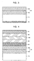
- FIG. 3 schematically shows a cross-sectional view of an optical device having an anti-reflective layer.
- the anti-reflective layer 70 is formed on one surface of the light transparent substrate 10, and the light control layer 20 consisting of the first layer 30 and the second layer 40 is formed on the other surface of the light transparent substrate 10, wherein the first layer 30 has a refractive index higher than that of the light transparent substrate 10, and the second layer 40 has a refractive index lower than that of the first layer 30.
- the refractive index of the first layer 30 is above that of the electrode layer 60, so that significant reflection does not occur until the light emitting from the emission layer becomes incident into the light control layer 20.
- the light diffusing from the emission layer as a spherical-wave-shaped wavefront is not subject to the significant reflection but incident into the light control layer 20 to be converted into a plane-wave-shaped wavefront.
- the interface between the air layer and the light transparent substrate 10 is subject to the significant reflection, and it is effective to arrange the anti-reflective layer at the interface, however, when it is arranged in other position, it may cause the converting efficiency from the spherical-wave-shaped wavefront to the plane-wave-shaped wavefront to be lowered.
- FIG. 4 schematically shows a cross-sectional view of an inorganic EL device using a light-emitting device substrate in accordance with a second embodiment.
- a light control layer 20 is formed on one surface of a light transparent substrate 10, and on top of that, an electrode layer 60, an insulating layer 90, an inorganic layer 100, an insulating layer 90, and an electrode layer 61 are sequentially formed.
- the light control layer 20 consists of the first layer 30 and the second layer 40 which are sequentially formed from the light transparent substrate 10, wherein the refractive index of the first layer 30 is higher than that of the light transparent substrate 10, and the refractive index of the second layer 40 is lower than that of the first layer 30.
- the first layer 30 is positioned on the light transparent substrate 10.
- any of well known configuration or constitutional material for the same may be employed.
- a spherical-wave-shaped wavefront emitted from the emission layer 100 to all directions is converted into a plane-wave-shaped wavefront in the light control layer 20.
- the light may be effectively extracted outside the substrate.
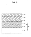
- FIG. 5 schematically shows a cross-sectional view of a structure of the organic EL device in accordance with the present embodiment.
- An anode 80, an emission layer 130, and a cathode 120 are sequentially formed on the light-emitting device substrate 50 in accordance with the present embodiment.
- FIG. 6 schematically shows a cross-sectional view of another structure of an organic EL device in accordance with the present embodiment.
- An anode 80, a hole transporting layer 140, an emission layer 130, and a cathode 120 are sequentially formed on the light-emitting device substrate 50 in accordance with the present embodiment.
- a structure consisted of anode/hole transporting layer/emission layer/electron transporting layer/cathode, or structure consisted of anode/emission layer/electron transporting layer/cathode may be employed.
- the organic EL device in accordance with the present embodiment may be any of a small molecular type and a polymer type.
- the light-emitting device substrate 50 of the organic EL device in accordance with the present embodiment is arranged to allow the light emitting from the emission layer to transmit the light-emitting device substrate 50.
- triphenyldiamine base molecule such as bis(di(P-tril)aminophenyl)-1,1-cyclohexane, N-N'-diphenyl-N, N'-bis(3-metylphenyl)-1,1'-biphenyl-4,4'-diamine, N, N'-diphenyl-N-N-bis(1-naphtyl)-1,1'-biphenyl)-4,4'-diamine or starburst type molecule may be used.
- triphenyldiamine base molecule such as bis(di(P-tril)aminophenyl)-1,1-cyclohexane, N-N'-diphenyl-N, N'-bis(3-metylphenyl)-1,1'-biphenyl-4,4'-diamine, N, N'-diphenyl-N-N-bis(1-naphtyl
- oxadizol derivative such as 2-(4-biphenyl)-5-(4-t-butylphenyl)-1,3,4-oxadiazole, bis ⁇ 2-(4-t-butylphenyl)-1,3,4-oxadiazole ⁇ -m-phenylene, triazol derivative, quinolinol metal complex may be used, however, not limited to these examples.
- charge transporting material doped with fluorescent material may be used for the light emitting material.
- the quinolinol metal complex such as Alq3 doped with quinacridone derivative such as 4-dicyanomethylene-2-methyl-6-(p-dimetylaminostyril)-4H-pyran (DCM), 2,3-quinacridone[7], doped with qumarine derivative such as 3-(2'-benzotiazol)-7-diethylaminoqumarine, or the electron transporting material of bis(2-metyl-8-hydroxyquinoline)-4-phenylphenol-aluminum complex doped with condensation polycyclic aromatic such as perylene, or the hole transporting material of 4,4'-bis(m-trilphenylamino)biphenyl (TPD) doped with rubrene may be used.
- quinacridone derivative such as 4-dicyanomethylene-2-methyl-6-(p-dimetylaminostyril)-4H-pyran (DCM), 2,3-quinacridone[7]
- qumarine derivative such as 3-(2'-benz
- the anode 80 is responsible for injecting holes into the hole transporting layer and preferably has a work function of 4.5eV or more.
- Specific example of the anode 80 material used in the present embodiment may include Indium Tin Oxide (ITO), NESA, gold, silver, platinum, copper, however, ITO is preferable.
- the refractive index of the second layer 40 and the refractive index of the anode 80 of the organic EL device may be different from each other, and it is preferable to have the refractive index of the second layer 40 higher than that of the anode 80 when the second layer 40 in contact with the anode layer 80.
- a material having a low value of work function for the purpose of injecting electrons into the electron transporting band or the emission layer is preferably used for the cathode 120.
- the material for the cathode 120 is not specifically limited, however, indium, aluminum, magnesium, magnesium-indium alloy, magnesium-aluminum alloy, aluminum-lithium alloy, aluminum-scandium-lithium alloy, or magnesium-silver alloy may be used for the same.
- the organic EL device in accordance with the present embodiment may be used as the passive drive type, or the active drive type by adding an active device such as TFT.
- the method for forming each layer of the organic EL device in the present embodiment is not specifically limited but selected from well-known methods. For example, vacuum deposition, molecular beam epitaxy (MBE), or dipping of solution resolved with a solvent, spin coating, casting, bar coating, roll coating may be used.
- the light control layer 20 converts the spherical-wave-shaped wavefront emitted from the emission center of the emission layer to the plane-wave-shaped wavefront. With this function, the light that has transmitted the light control layer 20 has the plane-wave-shaped wavefront, and propagates into the light transparent substrate 10 in a state of having directivity.
- the function of filter may be effectively used because of configuration described above. In other words, the light emitted from the emission layer is suppressed from propagating into an adjacent pixel, which leads to maintain color purity.
- the filter may be arranged on any surface of the light-emitting device substrate in accordance with the present embodiment, and the display may maintain high color purity even when the filter is arranged on the side opposite to the emission layer of the light-emitting device substrate.
- the process for fabricating the color converting filter or the color filter may be facilitated, which is separate from the process for fabricating the electrode or the emission layer. For example, it is possible to form the color converting filter or the color filter after the light-emitting device is formed.
- any kinds of the color converting filter or light emitting color of the emission layer may be used.
- a red converting filter for converting a blue color into a red color and a green converting filter for converting the blue color into a green color may be flatly arranged using a blue emission layer to thereby implement full color.
- FIG. 7 schematically shows a cross-sectional view of an organic EL device having a color converting filter.
- a red converting filter 510 and a green converting filter 511 are arranged on one surface of a light transparent substrate 10, and a light control layer 20, an anode 80, a blue emission layer 150, and a cathode 120 are sequentially arranged on the other surface of the light transparent substrate.
- the blue emitting light 501 is converted into a red emitting light 503 in the red converting filter and into a green emitting light 502 in the green converting filter.
- the blue emitting light may directly emit without any filters, or the light may emit through the color filter formed to improve purity.
- the light that has transmitted the light control layer 20 has a plane-wave-shaped wavefront, and propagates into the light transparent substrate 10 in a state of directivity, so that display without uneven color may be implemented even when each pixel size of red, green, blue colors becomes fine.
- FIG. 8 schematically shows a cross-sectional view of an organic EL device having a color filter.
- a full color display may be implemented with red, green, blue color filters by means of white emission layer.
- a red color filter 520, a green color filter 521, and a blue color filter 522 are arranged on one surface of a light transparent substrate 10, and a light control layer 20, anode 80, a white emission layer 160, and a cathode 120 are sequentially arranged on the other surface of the light transparent substrate.
- White color light emitting from the white emission layer are separated into red emitting light 503, green emitting light 502, and blue emitting light 501 at the red color filter 520, the green color filter 521, and the blue color filter 522, respectively.
- the light that has transmitted the light control layer 20 has a plane-wave-shaped wavefront, and propagates into the light transparent substrate 10 in a state of directivity, so that display without uneven color may be implemented even when each pixel size of red, green, blue colors becomes fine.
- the light-emitting device substrate in accordance with the present embodiment may be used as the encapsulating material of the organic EL device.
- the light-emitting device substrate is arranged to allow light emitting from the emission layer to transmit the light-emitting device substrate in the organic EL device in accordance with the present embodiment as mentioned above.
- the light-emitting device substrate may be used as the encapsulating material in accordance with the present embodiment.
- it is used as the encapsulating material it is preferable to attach the light-emitting device substrate to the utmost surface of the light-emitting device under reduced pressure.
- FIG. 4 to FIG. 8 shows a layer structure of a light-emitting device portion, however, this structure actually has a light-emitting device drive circuit such as TFT in the light transparent substrate 10.
- FIG. 9 schematically shows a cross-sectional view of an organic EL device having TFT.
- a TFT device portion 530 is formed in a drive circuit forming region of the light transparent substrate 10.
- a light-emitting device forming region of the light transparent substrate 10 has a light-emitting device consisting of a light control layer 20, an anode 80, an emission layer 130 and a cathode 120.
- the layer structure of the light-emitting device is not limited to the shown example and may be varied.
- color filter or color converting filter is not shown in the same figure. In this case, when a high refractive layer is present in a pixel display portion of the TFT substrate, the high refractive layer may be used as the first layer 30.
- the luminescence property of the organic EL device is as follows in examples to be described below.
- a luminance meter (TOPCON BM-5A) is arranged in a normal direction of the substrate with the focusing angle of 0.1°.
- the emission area of the organic EL device is 4mm 2 , and a direct current voltage is applied to the device to measure the current efficiency when the luminance is 100cd/ m 2 .
- the thickness of the light transparent substrate to be used is all 0.7mm.
- Melted quartz having a refractive index of 1.457 is used as the light transparent substrate, and a first layer of a light control layer is deposited with TiO 2 by means of sputtering to have a refractive index of 2.30 and a thickness of 700nm on one surface of the light transparent substrate, and on top of that, a second layer of the light control layer is deposited with TiO 2 /SiO 2 by means of sputtering to have a refractive index of 1.99 and a thickness of 378nm, which forms the light-emitting device substrate.
- ITO as an anode is deposited on the light-emitting device substrate by means of sputtering to have a sheet resistance of 20 ⁇ / ⁇ .
- the layer thickness of ITO is 100nm and the refractive index of the same is 1.78.
- a hole transporting layer of N,N'-bis(3-methylphenyl)-N,N'-diphenyl-[1,1'-biphenyl]-4,4'-diamine is first formed by vacuum deposition to have a thickness of 50nm, an emission layer of tris(8-quinolinorat)aluminum is then formed by the vacuum deposition to have a thickness of 70nm.
- a cathode of a magnesium-silver alloy is codeposited by the vacuum deposition at a deposition rate of 9:1 to have a thickness of 150nm, which forms the organic EL device of green emitting light (which has a peak wavelength of 530nm).
- the current efficiency is 7.0cd/A, which is about 2.3 times compared to the result of a first comparative example.
- the layer thickness of the TiO 2 is changed to be 200nm in the organic EL device manufactured in the first example.
- the current efficiency becomes 6.3cd/A, which exceeds the result of the first comparative example.
- the layer thickness of the TiO 2 is changed to be 2000nm in the organic EL device manufactured in the first example.
- the current efficiency becomes 4.9cd/A, which exceeds the result of the first comparative example.
- the layer thickness of the TiO 2 /SiO 2 is changed to be 200nm in the organic EL device manufactured in the first example.
- the current efficiency becomes 6.0cd/A, which exceeds the result of the first comparative example.
- the layer thickness of the TiO 2 /SiO 2 is changed to be 3000nm in the organic EL device manufactured in the first example.
- the current efficiency becomes 4.0cd/A, which exceeds the result of the first comparative example.
- the layer thickness of the TiO 2 is changed to be 116nm, and the layer thickness of the TiO 2 /SiO 2 is changed to be 134nm in the organic EL device manufactured in the first example.
- the current efficiency becomes 3.6cd/A, which exceeds the result of the first comparative example.
- the layer structure and fabrication method same as the first example have been performed to form the organic EI device except forming the light control layer.
- the current efficiency of this device is 3.0cd/A.
- the layer structure and fabrication method same as the first comparative example have been performed to form the organic EL device except that only the second layer of TiO 2 having a refractive index of 2.30 is deposited on the light transparent substrate by means of sputtering to have a thickness of 378nm without having the first layer of the light control layer.
- the current efficiency of this device is 2.9cd/A.
- the layer structure and fabrication method same as the first comparative example have been performed to form the organic EL device except that only the first layer of TiO 2 /SiO 2 composite layer having a refractive index of 2.30 is deposited on the light transparent substrate by means of sputtering to have a thickness of 700nm without having the second layer of the light control layer.
- the current efficiency of this device is 2.4cd/A.
- the layer structure and fabrication method same as the first example have been performed to form the organic EL device except that the thickness of TiO 2 layer (namely, the first layer) is 15nm.
- the current efficiency of this device is 2.9cd/A and no improvement for the light extraction efficiency has been observed. In this example, it is expected that no improvement be resulted from the extremely thin first layer, which causes interfaces of the first layer and the second layer not to sufficiently perform the wavefront converting function, and the resultant light extraction efficiency not to be improved.
- the layer structure and fabrication method same as the first example have been performed to form the organic EL device except that soda glass having a refractive index of 1.512 is used as the light transparent substrate and the light control layer is not present.
- the current efficiency of this device is 3.0cd/A.
- the layer structure and fabrication method same as the first example have been performed to form the organic EL device except that SiO 2 having a refractive index of 1.25 is used as the second layer of the light control layer by means of a sol-gel method.
- the luminous efficiency of the organic EI device is 3.1 cd/A, however, several spots that do not emit light (namely, dark spots) have been observed.
- the layer structure and fabrication method same as the first example have been performed to form the organic EL device except that an anti-reflective layer is formed instead of the light control layer.
- a composite layer of TiO 2 /SiO 2 having a refractive index of 1.59 is formed to have a thickness of 84nm by sputtering to be used as the anti-reflective layer.
- the current efficiency of this device is 2.8cd/A, and no improvement has been observed. It became obvious that the light extraction efficiency can not be sufficiently increased by the anti-reflective layer in consideration of its own function when it is formed in the organic EL device.
- the refractive index of the first layer is n1
- its layer thickness is d1
- the refractive index of the second layer is n2
- its layer thickness is d2
- the refractive index of anode is n3.
- the refractive index of the light transparent substrate is n(sub).
Landscapes
- Physics & Mathematics (AREA)
- Optics & Photonics (AREA)
- Electroluminescent Light Sources (AREA)
- Led Devices (AREA)
Description
- The present invention relates to an inorganic or organic electroluminescent (EL) device.
- An organic electroluminescent (EL) device is an emissive device using a principle that a fluorescent material emits light by means of recombination energy of holes injected from an anode and electrons injected from a cathode when an electric field is applied thereto. Researches have been conducted with regard to the organic EL device comprised of organic material after a stacked type low voltage driving organic EL device was disclosed in the art. Tang et al uses tris(8-quinolinol)aluminum for an emission layer, and uses triphenyldiamine for a hole transporting layer. The stacked type structure has an advantage in that efficiency of injecting the hole into the emission layer may be increased, efficiency of forming an exciton resulted from recombination by blocking the electron injected from the cathode may be increased, and the exciton formed in the emission layer may be blocked. For the structure of the organic EL device as mentioned above, two-layer type of a hole transporting (injecting) layer and a hole transportable emission layer, or three-layer type of a hole transporting (injecting) layer, an emission layer and an electron transporting (injecting) layer are well known in the art. In order to increase the recombination efficiency of the injected electron and hole in the stacked type device, researches for the device structure or a method for forming the same are conducted. However, the organic EL device has a limitation for the probability of singlet generation due to dependency of spin statistics when carriers are recombined, which causes to have an upper limit of a luminescence probability. The value of this upper limit is known to be about 25%.
- In the surface emitting device having spherical-wave-shaped wavefront such as the organic EL device with at least emission layer interposed between an anode and a cathode, a refractive index of the luminous body is higher than a substrate or air, so that the light of an exiting angle more than a critical angle is totally reflected at a substrate/air interface or the like, which causes the light not to be extracted outside the substrate. It is expected that only 20% of the total amount of light emitted is available when the refractive index of the luminous body is 1.6. As such, energy converting efficiency becomes low, which is limited to be about 5% in total when singlet formation probability is added to. In the organic EL device that has a luminescence probability highly limited, low light extraction efficiency as mentioned above causes degradation of the energy converting efficiency, which may be severely and adversely affected.
- As for the technique of improving the light extraction efficiency, several proposals have been suggested in the prior art.
- Japanese patent publication No.
S63 - 314795 - Japanese patent publication No.
H01 - 220394 - Japanese patent publication No.
2001 - 202827 - Japanese patent publication No.
2003 - 31374 FIG. 1 shows an optical multilayer body 2 comprised of a high refractive layer H1, a low refractive layer L1, and an anode layer 2A as a high refractive layer in this order between a substrate 1 made of a glass and an organic EL layer 3. And paragraph number [0025] thereof describes that the optical multilayer body 2 has an anti-reflective property and the light extraction efficiency from the substrate 1 is improved. - When the anti-reflective layer is formed of a single layer, reflective light is canceled off by light interference when nd = λ/4 (wherein d is thickness of physical layer and λ is wavelength to used) is met. The invention of the above-mentioned disclosure relates to one kind of such anti-reflective layer, and has a multi layered structure. Thickness of the high refractive layer H1, low refractive layer L1 and anode electrode layer 2A are 14.2nm, 41.5nm, and 139.8nm, respectively, and the thickness of each layer is set to be not more than half wavelength of the emission wavelength of 400 to 700nm in the structure described in its embodiment (see paragraph No. 0015). The multi layer described in this publication is one kind of so called anti-reflective layer.
- However, these prior arts still need to be improved.
- The method for forming lens or reflective surface on a substrate described in Japanese patent publication No.
1989 - 314795 2001 - 220394 - The method for interposing a low refractive layer between a substrate and an electrode layer as described in Japanese patent publication No.
2001 - 202827 - The method for arranging the anti-reflective layer as described in the Japanese patent publication No.
2003 - 31374 - In addition, as is well known in the art, the anti-reflective layer is highly dependent on wavelength, so that the light extraction efficiency is greatly varied due to the emission wavelength. Because of this factor, when the technique described in the same publication is applied to a white emitting device, the amount of light emitted outside the substrate is dependent on wavelength, which causes the amount to be greatly different from one another based on the wavelength, so that white balance is degraded.
- Furthermore, the anti-reflective layer is one that uses light interference to cancel off the light reflection, it needs to be formed to have its layer thickness or refractive index met with predetermined conditions. Thus, when the layer thickness is finely varied according to fabrication factors, the reflectivity of the anti-reflective layer is varied, which readily causes variation of the device performance.
- Development of the light extraction technique is of major interest for applying it to a low voltage drive of light-emitting device such as organic EL device, and is inevitable for implementing low power consumption of the device.
-
WO 02/37580 A1 microstructured element 530 including two first layers 532 and 534 is disposed between a transparent substrate 538 and an assembly consisting of electrodes 524, 528 and an emissive layer 526 sandwiched by the electrodes 524, 528 (see p. 15, II. 22 to p. 16, I. 9; Fig. 5(b)). One of the layers 532, 534 is a microstructured film and the other is adhesive or other material used to fill in the microstructured surface of the film. The refractive index of layer 534, which is sandwiched by the transparent substrate 538 and the layer 532, may be higher that the refractive index of layer 532. The refractive index of layer 532, which is sandwiched by the layer 534 and the electrode 528, may be the same or higher than the refractive index of the electrode 528. -
EP 1 178 709 A1 relates to an organic EL display inter alia including a color filter. -
US 6,392,338 B1 deals with another organic EL device inter alia including an assembly of an organic semiconductor layer 14E, transparent electrode 13E, dielectric layer 12E and glass substrate 11E. The refractive index of the dielectric layer12E is higher than that of the transparent electrode 13E. -
US 2002/0094422 A1 discloses a light-emitting device including a composite film layer between the electrode and substrate. In the composite film layer a refractive index decreases from the electrode toward the substrate. - It is, therefore, an object of the present invention to provide a light-emitting device substrate having good light extraction efficiency, and the light-emitting device using the same, which has overcome the problems of the prior art as mentioned above.
- As is described in the prior art, providing a focusing property to the substrate, or forming an anti-reflective layer between the substrate and the emission region has been proposed. Inventors of the present invention have researched the problems in other terms of the above-mentioned proposals to thereby succeed, thus remarkably improving the light extraction efficiency. In other words, the inventors have arranged a light control portion on the light transparent substrate, which performs wavefront conversion of the emitting light to be guided into the light transparent substrate to thereby complete the present invention of capable of improving the light extraction efficiency.
- According to the present invention, there is provided a light-emitting device, which comprises a light transparent substrate; a first layer formed on the light transparent substrate and having a refractive index higher than that of the substrate; a second layer formed on the first layer and having a refractive index lower than that of the first layer, wherein the layers have a refractive index distribution; an electrode layer formed on the second layer and having a refractive index lower than that of the second layer; and an emission layer formed on the electrode layer wherein
- a) an optical thickness of the first layer is given such that n1 x d1 ≥ λ/2 is met, wherein a peak emission wavelength of the emission layer is λ, the refractive index of the first layer is n1, and its thickness is d1; and/or
- b) an optical thickness of the second layer is given such that n2 x d2 ≥ λ/2 is met, wherein the peak emission wavelength of the emission layer is λ, the refractive index of the second layer is n2, and its thickness is d2.
- Color converting filters or color filters may be arranged on a surface of the light transparent substrate. Light emitted from the emission layer may be a single color light, especially blue light. The light-emitting device may be an organic EL device. A combination of the first layer and the second layer is denoted in the following as a light control portion.
- According to the present invention, the light extraction efficiency is remarkably increased by the light control portion formed on the light transparent substrate. The light control portion converts the spherical wave shaped light emitted from its upper portion into the plane-wave-shaped light to be guided into the light transparent substrate. Since the plane-wave-shaped light is guided into the light transparent substrate, light reflection or loss between the light transparent substrate and its adjacent layer may be effectively reduced, which leads to remarkably improve the light extraction efficiency.
- In this case, "the plane-wave-shaped light" means that point vector of the light is approximately even. Light phase in a plane vertical to the light propagation direction may not be necessarily present. "Wavefront conversion" means that the wavefront is converted to increase directivity of the light, which converts the spherical wave shaped light where the point vector is diffused into the plane-wave-shaped light as mentioned above. Several shapes may be employed for the configuration of wavefront conversion into the plane-wave-shaped light. For example, the wavefront conversion may be performed by introducing a refractive index varying region in the light control portion and properly adjusting the light propagation.
- In addition, the "light-emitting device substrate" means one that is used with an emission region mounted on an upper portion of the light control portion. Several shapes may be employed for the emission region.
- In the present invention, the light control portion is arranged on the light transparent substrate and consists of light control layers, some of the light control layers having refractive index distribution.
- As mentioned above, the light control portion having a wavefront converting function is arranged within the layer structure forming the device, which leads to remarkably improve the light extraction efficiency. However, when such light control portion is arranged, a new light loss portion may be present within the layer structure. In this case, an effect of light control is reduced by the light loss. In other words, when the light control portion having the wavefront converting function is arranged, the above configuration becomes accompanied with a new problem. Therefore, the present invention provides the configuration as below to cope with the above problem.
- To detail this, the light control layer may have a configuration that distributes the refractive index, which becomes lower from the light transparent substrate toward its upper portion in accordance with the present invention.
- When the light propagates from the high refractive region to the low refractive region, light reflection or light loss occurs at the interface therebetween. In accordance with the above-mentioned configuration, when the emission region is formed on the light control layer to allow the light to emit from the light transparent substrate, the refractive index becomes lower along the propagation direction of the light. Therefore, the above-mentioned interface where the light reflection or light loss occurs is not present, which leads to remarkably improve the light extraction efficiency. In the refractive index distribution of the configuration where the refractive index is reduced from the light transparent substrate toward its upper portion, however, step shaped or continuous shaped distribution may also be employed.
- In the present invention, the light-emitting device substrate further comprises an electrode layer on the light control layer, and a refractive index near the upper surface of the light control layer may be higher than that of the electrode layer. In accordance with this configuration, light reflection or light loss in the interface between the light control layer and its upper portion is suppressed. In other words, the refractive index becomes reduced from the light control layer toward the electrode layer. Therefore, the light extraction efficiency becomes further improved.
- The light control layer includes a first layer formed on the light transparent substrate, and a second layer formed on the first layer and having a refractive index lower than that of the first layer.
- The interface between the first layer and the second layer becomes the wavefront converting region in accordance with this configuration. The wavefront of the light is converted in this interface, so that the spherical wave shaped light becomes the plane-wave-shaped light. Since the wavefront is performed at the interface of these layers, the plane-wave-shaped light is effectively and safely guided into the light transparent substrate, which leads to improve the light extraction efficiency.
- In this case, the first layer is preferably formed to be contacted with the light transparent substrate. With this configuration, the plane-wave-shaped light is guided into the light transparent substrate as it is, the light reflection or light loss in the interface between the light transparent substrate and its upper layer, which has been problems in the prior art, may be effectively suppressed.
- In addition, n1d1 ≥ λ/2 is met when the peak emission wavelength is λ, the refractive index of the first layer is n1 and its thickness is d1.
- In addition, n2d2≥ λ/2 is met when the refractive index of the second layer is n2 and its thickness is d2.
- With this configuration, the wavefront of the light is properly converted into the plane-wave-shaped light in the interface of the first and second layers, which leads to obtain the improved light extraction efficiency.
- A driving circuit for driving the light-emitting device may be arranged in the light transparent substrate in accordance with the present invention. For example, a device such as TFT may be formed.
- In addition, the upper direction is defined from the light transparent substrate toward the light control portion in the present invention.
- The above and other features and advantages of the present invention will become more apparent to those of ordinary skill in the art by describing in detail preferred embodiments thereof with reference to the attached drawings in which:
-
FIG. 1 to FIG. 3 schematically shows cross-sectional views of a substrate for a light-emitting device in accordance with a first embodiment of the present invention; -
FIG. 4 to FIG. 9 schematically shows cross-sectional views of a light-emitting device in accordance with a second embodiment of the present invention; and -
FIG. 10 shows an exemplary structure of a light control portion (not being part of the present invention). - The present invention will now be described more fully hereinafter with reference to the accompanying drawings, in which preferred embodiments of the invention are shown. The term "the refractive index" refers to as one of peak wavelength of light emitted from an emission layer, if not specifically described in the present specification. Like numbers refer to like devices throughout the specification to thereby omit description thereof.
- The light-emitting device substrate in accordance with the present invention may be applied to the light-emitting device that emits light resulting from an external stimulus such as voltage, and, for example, it may be applied to a light-emitting device such as organic EL device, inorganic EL device plasma display, and LED. In particular, the light-emitting device may have a remarkable effect on a device where the light is emitted from a point light source of an emission region. For example, light emission of EL device is collection of point light emission from the emission center of the emission layer, which leads to have a significant effect of the present invention.
- The present invention has the light extraction efficiency improved by means of a function of a light control layer. The operation of the light extraction efficiency is less dependent on wavelength than an anti-reflective layer. Thus, when it is applied to a white light-emitting device, the amount of light emitted outside the substrate is not significantly different from one another based on the wavelength, and white balance may be relatively maintained in a good state. In addition, variation of device performance due to a manufacturing factor or the like may be relatively suppressed, which may be the advantage of the present invention.
-
FIG. 1 schematically shows a cross-sectional view of a substrate for a light-emitting device in accordance with the present embodiment. To detail this, a light-emittingdevice substrate 50 of the present invention comprises alight control layer 20 on one side of a lighttransparent substrate 10. Thelight control layer 20 consists of afirst layer 30 having a refractive index higher than that of the lighttransparent substrate 10 and asecond layer 40 having a refractive index lower than that of thefirst layer 30, which are stacked onto the lighttransparent substrate 10 in this order. - This optical device substrate has an emission region above the
light control layer 20 and is used for a substrate of the light-emitting device. Thelight control layer 20 converts a spherical-wave-shaped wavefront introduced from its upper direction to a plane-wave-shaped wavefront. A center of the emission layer such as organic EL device is treated as a point light source, and light emitting from the point light source propagates to all directions of 360°. In only a typical light transparent substrate, the spherical-wave-shaped wavefront emits from the emission center outside the substrate, and an exiting angle above a critical angle is reflected within the substrate by total reflection and can not be emitted outside the substrate. However, at an interface between thefirst layer 30 and thesecond layer 40 in the present embodiment, the spherical-wave-shaped wavefront is converted into the plane-wave-shaped wavefront to thereby be light having high directivity. By means of this configuration, the spherical-wave-shaped wavefront emitted from the point light source is converted into to the plane-wave-shaped wavefront after it passes through thelight control layer 20, and passes the lighttransparent substrate 10 while maintains the directivity. As a result, an amount of total reflection light is small, and a lot of light are emitted by the outside of the lighttransparent substrate 10, which leads to improve light extraction efficiency. The light emitting outside the substrate is not the spherical or cylindrical-wave-shaped wavefront but the plane-wave-shaped wavefront. Each layer consisting of the light-emitting device substrate in accordance with the present invention is optically planarized, and a thin film material having high mechanical intensity may be selected for the layer, so that the light-emitting device having high reliability may be provided. In other words, an electrical short circuit due to unevenness of the substrate surface may be suppressed from occurring, and a crack of the thin film due to the substrate disformation may also be suppressed. -
FIG. 2 shows a cross-sectional view of a substrate where anelectrode layer 60 is arranged on the upper surface of the light-emittingdevice substrate 50 ofFIG. 1 . Theelectrode layer 60 has a refractive index lower than that of thesecond layer 40. - In order to improve the light extraction efficiency in this light-emitting device substrate, two interfaces perform a major function. One is the interface between the light
transparent substrate 10 and thefirst layer 30, and the other is the interface between thefirst layer 30 and thesecond layer 40. In these interfaces, light diffusing from the emission layer as the spherical-wave-shaped wavefront may be converted into the plane-wave-shaped wavefront. Therefore, configuration of these two interfaces and configuration of introducing light into these interfaces are important in accordance with the present embodiment. In the configuration of the present invention, light emitting from the emission layer passes through theelectrode layer 60, and continues to pass through thesecond layer 40,first layer 30, and finally the lighttransparent substrate 10 to be emitted outside the lighttransparent substrate 10. Therefore, the refractive index continues to be higher from theelectrode layer 60 to the lighttransparent substrate 10 and becomes lower from the lighttransparent substrate 10 in the present invention, as is shown with a relative value of refractive index inFIG. 2 . - As mentioned above, when an interface is present where light propagates from a high refractive layer to a low refractive layer, light reflection or loss occurs in the interface. Such interface is not present in the configuration from the
electrode layer 60 to thelight control layer 20 inFIG. 2 , which leads to implement good light extraction efficiency. - Hereinafter, each portion forming the light-emitting
device substrate 50 will be described in detail in accordance with the present embodiment. - The light
transparent substrate 10 is used as a light extraction substrate of a light-emitting device. It transmits some wavelengths in at least a visible light band. The lighttransparent substrate 10 in the present embodiment may allow at least some light of wavelength 400 to 800nm to be transmitted, and organic or inorganic material may be used for the same. Glass or the like may be used for the inorganic material, and plastic or the like may be used for the organic material. The glass may include melted quartz, non-alkali glass, soda glass, or optical glass such as heavy print glass. The plastic may include engineering plastic such as polyethylsulphon (PES), polyethyleneterephtalate (PET). The refractive index of the lighttransparent substrate 10 is preferably 1.4 to 2.1. A barrier layer for suppressing moisture or oxygen from being transmitted may be coated on the lighttransparent substrate 10. In addition, color converting filter or color filter may be attached to the same. The thickness of the lighttransparent substrate 10 is not specifically limited, however, about 0.1 to 2 mm is preferable in terms of utility. - The substrate shown in
FIG. 1 and FIG. 2 is the light-emitting device substrate, and a driving circuit for the light-emitting device is formed on the lighttransparent substrate 10.FIG. 9 shows a schematic structure of an organic EL device having thin film transistor (TFT). ATFT device portion 530 is formed on the lighttransparent substrate 10. The substrate in accordance with the present embodiment is preferably used for such device portion. - The light-emitting
device substrate 50 in accordance with the present invention is manufactured to sequentially stack thefirst layer 30 and thesecond layer 40 on the lighttransparent substrate 10. An optical device in accordance with the present embodiment is manufactured to stack at least anelectrode layer 60 and an emission layer on the light-emittingdevice substrate 50. As such, when the lighttransparent substrate 10 has an uneven portion on its surface, this uneven portion affects theelectrode layer 60 or the emission layer, which may cause an electrical short circuit. Therefore, even substrate is preferably used as the lighttransparent substrate 10. Furthermore, an active matrix driving substrate is preferably even at least in a pixel portion for operating the light-emitting device. - The
first layer 30 has a refractive index higher than that of the lighttransparent substrate 10. For example, when the refractive index of the lighttransparent substrate 10 is 1.45, the refractive index of thefirst layer 30 is practically and preferably higher than 1.45 to be in a range between about 1.46 to about 2.5. A ratio of the refractive index of thefirst layer 30 with respect to that of the light transparent substrate 10 (that is, refractive index of thefirst layer 30 / refractive index of the light transparent substrate 10) is preferably high. The ratio is more than 1, preferably 1.15 or more, and more preferably 1.3 or more. As a result, the lighttransparent substrate 10 having a refractive index of about 1.45 may be used, which has high general usage, and the light control layer capable of significantly performing a wavefront converting function may be formed on the light transparent substrate. - When the peak wavelength of light emitting from the emission layer is λ(µm) and the refractive index of the
first layer 30 is n1 and its thickness is d1, the optical thickness of thefirst layer 30, namely, n1d1 is preferably above 0.5 λ, and more preferably above λ. As a result, the light incident from thesecond layer 40 is preferably subject to wavefront conversion to be a plane-wave-shaped light, which allows to reliably implement an improving effect of the light extraction efficiency. As for the upper limit of n1d1, its value is preferably not more than 10 λ. As a result, the wavefront conversion into the plane-wave-shaped light may be reliably implemented. - Organic or inorganic material may be used for forming the
first layer 30 of the light-emitting device substrate. Polyimide, polyurethane or the like may be used for the organic material, and SiO2, TiO2, SiNx, Al2O3, Ta2O5, ZrO2, CeO2, Y2O3, MgO, Nb2O5, ITO or the like may be used for the inorganic material. Only one of them or combination of at least two kinds of materials may be used. It is preferable that the inorganic material is used in consideration of thermal stability or the like. - The
first layer 30 may preferably allow some portion of wavelength of 400 to 800nm to be transmitted. Optical thin films of them may be manufactured by a wet or dry forming method. The wet forming method may include sol-gel method or the like, and the dry forming method may include chemical vapor deposition (CVD) or physical vapor deposition such as deposition, plasma sputtering and ion beam sputtering. To detail this, the CVD method may include PECVD, MOCVD, laser CVD, photochemical CVD and electron cyclotron resonance CVD. In addition, the deposition may include resistive heating evaporation, electron beam deposition, laser deposition, arc discharge deposition, RF heating deposition or the like. The plasma sputtering may include direct current sputtering, RF sputtering, counter target sputtering, magnetron sputtering or the like. In addition, an ion source of the ion beam sputtering may include penning type, hollowcathode type and duo plasmatron type or the like. - The
second layer 40 has a wavefront converting function as thefirst layer 30 does. - When refractive indices of the
first layer 30, thesecond layer 40, and theelectrode layer 60 are n1, n2, n3, respectively, these indices are set to be n1 ≥n2≥n3. For example, when the refractive index of thefirst layer 30 is 2.4 and that of theelectrode layer 60 is 1.75, the refractive index of thesecond layer 40 is present therebetween. The value of the n1/n2 is above 1, preferably 1.1 or more, and more preferably 1.25 or more. - When the peak wavelength of light emitting from the emission layer is λ (µm) and the refractive index of the
second layer 40 is n2 and its thickness is d2, the optical thickness of thesecond layer 40, namely, n2d2 is preferably above 0.5 λ, and more preferably above λ. As a result, the light emitting from thesecond layer 40 is preferably subject to wavefront conversion to be a plane-wave-shaped light at an interface between thefirst layer 30 and thesecond layer 40, which allows to reliably implement an improving effect of the light extraction efficiency. As for the upper limit of n2d2, its value is preferably not more than 10 λ. As a result, wavefront conversion into the plane-wave-shaped light may be reliably implemented. In addition, the refractive index of the second layer is preferably not less than 1.35. When the refractive index of the second layer is too low, density of the second layer may be too lowered to fail to obtain sufficient mechanical intensity. - Organic or inorganic material may be used for forming the
second layer 40 of the light-emitting device substrate. Polyimide, polyurethane or the like may be used for the organic material, and SiO2, TiO2, SiNx, Al2O3, Ta2O5, ZrO2, CeO2, Y2O3, MgO, Nb2O5, ITO or the like may be used for the inorganic material. Only one of them or combination of at least two kinds of them may be used. It is preferable that the inorganic material is used in consideration of thermal stability or the like. - The
second layer 40 may preferably allow some portion of wavelength of 400 to 800nm to be transmitted. Optical thin films of them may be manufactured by a wet or dry forming method. The wet forming method may include sol-gel method or the like, and the dry forming method may include chemical vapor deposition (CVD) or physical vapor deposition such as deposition, plasma sputtering and ion beam sputtering. To detail this, the CVD method may include PECVD, MOCVD, laser CVD, photochemical CVD and electron cyclotron resonance CVD. In addition, the deposition may include resistive heating evaporation, electron beam deposition, laser deposition, arc discharge deposition, RF heating deposition or the like. The plasma sputtering may include direct current sputtering, RF sputtering, counter target sputtering, magnetron sputtering or the like. In addition, an ion source of the ion beam sputtering may include penning type, hollowcathode type and duo plasmatron type or the like. - In this case, the
second layer 40 is formed after thefirst layer 30 is formed, so that the method for forming film is preferably selected which does not resolve thefirst layer 30. - In addition, a material suitable for a process for fabricating the electrode layer or the emission layer to be formed on the
first layer 30 and thesecond layer 40 needs to be selected for the first and second layers. - In the present embodiment, the
first layer 30 or thesecond layer 40 may act as an auxiliary electrode for lowering resistance of theelectrode layer 60. These layers may not only contribute to optical properties but also electrical properties. When these layers are used as the auxiliary electrode, conductive material such as ITO is used for the constitutional material and is connected to theelectrode layer 60 to lower resistance of theelectrode layer 60. When thesecond layer 40 is used as the auxiliary electrode, it may be directly connected to theelectrode 60, and when thefirst layer 30 is used as the auxiliary, it may be connected to theelectrode 60 through contact hole or the like. - The light-emitting device substrate in accordance with the present embodiment may include an anti-reflective layer. The anti-reflective layer in the first embodiment includes the anti-reflective layer at an interface where emitting light transmits the light-emitting
device substrate 50 and emits to the air, namely, at an interface between the air layer and the lighttransparent substrate 10, which leads to improve the light extraction efficiency.FIG. 3 schematically shows a cross-sectional view of an optical device having an anti-reflective layer. Theanti-reflective layer 70 is formed on one surface of the lighttransparent substrate 10, and thelight control layer 20 consisting of thefirst layer 30 and thesecond layer 40 is formed on the other surface of the lighttransparent substrate 10, wherein thefirst layer 30 has a refractive index higher than that of the lighttransparent substrate 10, and thesecond layer 40 has a refractive index lower than that of thefirst layer 30. In the first embodiment of the present invention, the refractive index of thefirst layer 30 is above that of theelectrode layer 60, so that significant reflection does not occur until the light emitting from the emission layer becomes incident into thelight control layer 20. Therefore, the light diffusing from the emission layer as a spherical-wave-shaped wavefront is not subject to the significant reflection but incident into thelight control layer 20 to be converted into a plane-wave-shaped wavefront. The interface between the air layer and the lighttransparent substrate 10 is subject to the significant reflection, and it is effective to arrange the anti-reflective layer at the interface, however, when it is arranged in other position, it may cause the converting efficiency from the spherical-wave-shaped wavefront to the plane-wave-shaped wavefront to be lowered. -
FIG. 4 schematically shows a cross-sectional view of an inorganic EL device using a light-emitting device substrate in accordance with a second embodiment. Alight control layer 20 is formed on one surface of a lighttransparent substrate 10, and on top of that, anelectrode layer 60, an insulatinglayer 90, aninorganic layer 100, an insulatinglayer 90, and anelectrode layer 61 are sequentially formed. Thelight control layer 20 consists of thefirst layer 30 and thesecond layer 40 which are sequentially formed from the lighttransparent substrate 10, wherein the refractive index of thefirst layer 30 is higher than that of the lighttransparent substrate 10, and the refractive index of thesecond layer 40 is lower than that of thefirst layer 30. Thefirst layer 30 is positioned on the lighttransparent substrate 10. In addition, any of well known configuration or constitutional material for the same may be employed. - In accordance with the present embodiment, a spherical-wave-shaped wavefront emitted from the
emission layer 100 to all directions is converted into a plane-wave-shaped wavefront in thelight control layer 20. As a result, the light may be effectively extracted outside the substrate. - This embodiment relates to a case when the light-emitting device substrate described in the first embodiment is applied to an organic EL device.
FIG. 5 schematically shows a cross-sectional view of a structure of the organic EL device in accordance with the present embodiment. Ananode 80, anemission layer 130, and acathode 120 are sequentially formed on the light-emittingdevice substrate 50 in accordance with the present embodiment. -
FIG. 6 schematically shows a cross-sectional view of another structure of an organic EL device in accordance with the present embodiment. Ananode 80, ahole transporting layer 140, anemission layer 130, and acathode 120 are sequentially formed on the light-emittingdevice substrate 50 in accordance with the present embodiment. Alternatively, a structure consisted of anode/hole transporting layer/emission layer/electron transporting layer/cathode, or structure consisted of anode/emission layer/electron transporting layer/cathode may be employed. Furthermore, the organic EL device in accordance with the present embodiment may be any of a small molecular type and a polymer type. In addition, the light-emittingdevice substrate 50 of the organic EL device in accordance with the present embodiment is arranged to allow the light emitting from the emission layer to transmit the light-emittingdevice substrate 50. - Various materials may be used for the hole transporting material. Specifically, triphenyldiamine base molecule such as bis(di(P-tril)aminophenyl)-1,1-cyclohexane, N-N'-diphenyl-N, N'-bis(3-metylphenyl)-1,1'-biphenyl-4,4'-diamine, N, N'-diphenyl-N-N-bis(1-naphtyl)-1,1'-biphenyl)-4,4'-diamine or starburst type molecule may be used.
- Various materials may be used for the electron transporting material. Specifically, oxadizol derivative such as 2-(4-biphenyl)-5-(4-t-butylphenyl)-1,3,4-oxadiazole, bis{2-(4-t-butylphenyl)-1,3,4-oxadiazole}-m-phenylene, triazol derivative, quinolinol metal complex may be used, however, not limited to these examples.
- For example, tris(8-quinolinol) aluminum complex (Alq3) or bisdiphenylvinylbiphenyl (BDPVBi), 1,3-bis(p-t-butylphenyl-1,3,4-oxadiazolil)phenyl (OXD-7), N, N'-bis(2,5-di-t-butylphenyl) perylenetetracarbonic acid dimide (BPPC), 1,4bis(p-tril-p-methylstyrilphenyl)naphthalene may be used for the light emitting material. Alternatively, charge transporting material doped with fluorescent material may be used for the light emitting material. For example, the quinolinol metal complex such as Alq3 doped with quinacridone derivative such as 4-dicyanomethylene-2-methyl-6-(p-dimetylaminostyril)-4H-pyran (DCM), 2,3-quinacridone[7], doped with qumarine derivative such as 3-(2'-benzotiazol)-7-diethylaminoqumarine, or the electron transporting material of bis(2-metyl-8-hydroxyquinoline)-4-phenylphenol-aluminum complex doped with condensation polycyclic aromatic such as perylene, or the hole transporting material of 4,4'-bis(m-trilphenylamino)biphenyl (TPD) doped with rubrene may be used.
- In devices shown in
FIG. 5 andFIG. 6 , theanode 80 is responsible for injecting holes into the hole transporting layer and preferably has a work function of 4.5eV or more. Specific example of theanode 80 material used in the present embodiment may include Indium Tin Oxide (ITO), NESA, gold, silver, platinum, copper, however, ITO is preferable. In addition, the refractive index of thesecond layer 40 and the refractive index of theanode 80 of the organic EL device may be different from each other, and it is preferable to have the refractive index of thesecond layer 40 higher than that of theanode 80 when thesecond layer 40 in contact with theanode layer 80. - In the meantime, a material having a low value of work function for the purpose of injecting electrons into the electron transporting band or the emission layer is preferably used for the
cathode 120. The material for thecathode 120 is not specifically limited, however, indium, aluminum, magnesium, magnesium-indium alloy, magnesium-aluminum alloy, aluminum-lithium alloy, aluminum-scandium-lithium alloy, or magnesium-silver alloy may be used for the same. In addition, the organic EL device in accordance with the present embodiment may be used as the passive drive type, or the active drive type by adding an active device such as TFT. The method for forming each layer of the organic EL device in the present embodiment is not specifically limited but selected from well-known methods. For example, vacuum deposition, molecular beam epitaxy (MBE), or dipping of solution resolved with a solvent, spin coating, casting, bar coating, roll coating may be used. - The
light control layer 20 converts the spherical-wave-shaped wavefront emitted from the emission center of the emission layer to the plane-wave-shaped wavefront. With this function, the light that has transmitted thelight control layer 20 has the plane-wave-shaped wavefront, and propagates into the lighttransparent substrate 10 in a state of having directivity. When color converting filter or color filter is formed, the function of filter may be effectively used because of configuration described above. In other words, the light emitted from the emission layer is suppressed from propagating into an adjacent pixel, which leads to maintain color purity. - The filter may be arranged on any surface of the light-emitting device substrate in accordance with the present embodiment, and the display may maintain high color purity even when the filter is arranged on the side opposite to the emission layer of the light-emitting device substrate. In general, it is difficult to form an electrode or emission layer on the color converting filter or color filter in terms of fabrication process. However, when the filter is arranged on the light
transparent substrate 10 opposite to the emission layer, the process for fabricating the color converting filter or the color filter may be facilitated, which is separate from the process for fabricating the electrode or the emission layer. For example, it is possible to form the color converting filter or the color filter after the light-emitting device is formed. When the color converting filter is used, any kinds of the color converting filter or light emitting color of the emission layer may be used. A red converting filter for converting a blue color into a red color and a green converting filter for converting the blue color into a green color may be flatly arranged using a blue emission layer to thereby implement full color. -
FIG. 7 schematically shows a cross-sectional view of an organic EL device having a color converting filter. A red convertingfilter 510 and a green convertingfilter 511 are arranged on one surface of a lighttransparent substrate 10, and alight control layer 20, ananode 80, ablue emission layer 150, and acathode 120 are sequentially arranged on the other surface of the light transparent substrate. The blue emitting light 501 is converted into a red emitting light 503 in the red converting filter and into a green emitting light 502 in the green converting filter. In this case, the blue emitting light may directly emit without any filters, or the light may emit through the color filter formed to improve purity. As mentioned above, the light that has transmitted thelight control layer 20 has a plane-wave-shaped wavefront, and propagates into the lighttransparent substrate 10 in a state of directivity, so that display without uneven color may be implemented even when each pixel size of red, green, blue colors becomes fine. -
FIG. 8 schematically shows a cross-sectional view of an organic EL device having a color filter. A full color display may be implemented with red, green, blue color filters by means of white emission layer. To detail this, ared color filter 520, agreen color filter 521, and ablue color filter 522 are arranged on one surface of a lighttransparent substrate 10, and alight control layer 20,anode 80, awhite emission layer 160, and acathode 120 are sequentially arranged on the other surface of the light transparent substrate. White color light emitting from the white emission layer are separated into red emitting light 503, green emitting light 502, and blue emitting light 501 at thered color filter 520, thegreen color filter 521, and theblue color filter 522, respectively. As mentioned above, the light that has transmitted thelight control layer 20 has a plane-wave-shaped wavefront, and propagates into the lighttransparent substrate 10 in a state of directivity, so that display without uneven color may be implemented even when each pixel size of red, green, blue colors becomes fine. - The light-emitting device substrate in accordance with the present embodiment may be used as the encapsulating material of the organic EL device. The light-emitting device substrate is arranged to allow light emitting from the emission layer to transmit the light-emitting device substrate in the organic EL device in accordance with the present embodiment as mentioned above. In the top emission type or reverse type of the organic EL device in which light emits from the emission layer into a direction opposite to the substrate where the
electrode layer 60 or the emission layer is formed, the light-emitting device substrate may be used as the encapsulating material in accordance with the present embodiment. When it is used as the encapsulating material, it is preferable to attach the light-emitting device substrate to the utmost surface of the light-emitting device under reduced pressure. -
FIG. 4 to FIG. 8 shows a layer structure of a light-emitting device portion, however, this structure actually has a light-emitting device drive circuit such as TFT in the lighttransparent substrate 10.FIG. 9 schematically shows a cross-sectional view of an organic EL device having TFT. ATFT device portion 530 is formed in a drive circuit forming region of the lighttransparent substrate 10. In the meantime, a light-emitting device forming region of the lighttransparent substrate 10 has a light-emitting device consisting of alight control layer 20, ananode 80, anemission layer 130 and acathode 120. The layer structure of the light-emitting device is not limited to the shown example and may be varied. In addition, color filter or color converting filter is not shown in the same figure. In this case, when a high refractive layer is present in a pixel display portion of the TFT substrate, the high refractive layer may be used as thefirst layer 30. - Hereinafter, the present invention will be described in detail based on the example. The luminescence property of the organic EL device is as follows in examples to be described below. A luminance meter (TOPCON BM-5A) is arranged in a normal direction of the substrate with the focusing angle of 0.1°. In addition, the emission area of the organic EL device is 4mm2, and a direct current voltage is applied to the device to measure the current efficiency when the luminance is 100cd/ m2. In addition, the thickness of the light transparent substrate to be used is all 0.7mm.
- Melted quartz having a refractive index of 1.457 is used as the light transparent substrate, and a first layer of a light control layer is deposited with TiO2 by means of sputtering to have a refractive index of 2.30 and a thickness of 700nm on one surface of the light transparent substrate, and on top of that, a second layer of the light control layer is deposited with TiO2/SiO2 by means of sputtering to have a refractive index of 1.99 and a thickness of 378nm, which forms the light-emitting device substrate.
- In addition, ITO as an anode is deposited on the light-emitting device substrate by means of sputtering to have a sheet resistance of 20Ω/□. The layer thickness of ITO is 100nm and the refractive index of the same is 1.78.
- Next, Two layers are formed on the ITO as an organic layer. A hole transporting layer of N,N'-bis(3-methylphenyl)-N,N'-diphenyl-[1,1'-biphenyl]-4,4'-diamine is first formed by vacuum deposition to have a thickness of 50nm, an emission layer of tris(8-quinolinorat)aluminum is then formed by the vacuum deposition to have a thickness of 70nm. Finally, a cathode of a magnesium-silver alloy is codeposited by the vacuum deposition at a deposition rate of 9:1 to have a thickness of 150nm, which forms the organic EL device of green emitting light (which has a peak wavelength of 530nm). As a result, the current efficiency is 7.0cd/A, which is about 2.3 times compared to the result of a first comparative example.
- The layer thickness of the TiO2 is changed to be 200nm in the organic EL device manufactured in the first example. The current efficiency becomes 6.3cd/A, which exceeds the result of the first comparative example.
- The layer thickness of the TiO2 is changed to be 2000nm in the organic EL device manufactured in the first example. The current efficiency becomes 4.9cd/A, which exceeds the result of the first comparative example.
- The layer thickness of the TiO2/SiO2 is changed to be 200nm in the organic EL device manufactured in the first example. The current efficiency becomes 6.0cd/A, which exceeds the result of the first comparative example.
- The layer thickness of the TiO2/SiO2 is changed to be 3000nm in the organic EL device manufactured in the first example. The current efficiency becomes 4.0cd/A, which exceeds the result of the first comparative example.
- The layer thickness of the TiO2 is changed to be 116nm, and the layer thickness of the TiO2/SiO2 is changed to be 134nm in the organic EL device manufactured in the first example. The current efficiency becomes 3.6cd/A, which exceeds the result of the first comparative example.
- The layer structure and fabrication method same as the first example have been performed to form the organic EI device except forming the light control layer. The current efficiency of this device is 3.0cd/A.
- The layer structure and fabrication method same as the first comparative example have been performed to form the organic EL device except that only the second layer of TiO2 having a refractive index of 2.30 is deposited on the light transparent substrate by means of sputtering to have a thickness of 378nm without having the first layer of the light control layer. The current efficiency of this device is 2.9cd/A.
- The layer structure and fabrication method same as the first comparative example have been performed to form the organic EL device except that only the first layer of TiO2/SiO2 composite layer having a refractive index of 2.30 is deposited on the light transparent substrate by means of sputtering to have a thickness of 700nm without having the second layer of the light control layer. The current efficiency of this device is 2.4cd/A.
- The layer structure and fabrication method same as the first example have been performed to form the organic EL device except that the thickness of TiO2 layer (namely, the first layer) is 15nm. The current efficiency of this device is 2.9cd/A and no improvement for the light extraction efficiency has been observed. In this example, it is expected that no improvement be resulted from the extremely thin first layer, which causes interfaces of the first layer and the second layer not to sufficiently perform the wavefront converting function, and the resultant light extraction efficiency not to be improved.
- The layer structure and fabrication method same as the first example have been performed to form the organic EL device except that soda glass having a refractive index of 1.512 is used as the light transparent substrate and the light control layer is not present. The current efficiency of this device is 3.0cd/A.
- The layer structure and fabrication method same as the first example have been performed to form the organic EL device except that SiO2 having a refractive index of 1.25 is used as the second layer of the light control layer by means of a sol-gel method. The luminous efficiency of the organic EI device is 3.1 cd/A, however, several spots that do not emit light (namely, dark spots) have been observed.
- The layer structure and fabrication method same as the first example have been performed to form the organic EL device except that an anti-reflective layer is formed instead of the light control layer. A composite layer of TiO2/SiO2 having a refractive index of 1.59 is formed to have a thickness of 84nm by sputtering to be used as the anti-reflective layer. The current efficiency of this device is 2.8cd/A, and no improvement has been observed. It became obvious that the light extraction efficiency can not be sufficiently increased by the anti-reflective layer in consideration of its own function when it is formed in the organic EL device.
- Evaluation results of the above-mentioned examples and comparative examples are shown below. In the tables shown below, the refractive index of the first layer is n1, its layer thickness is d1, the refractive index of the second layer is n2, its layer thickness is d2, and the refractive index of anode is n3. In addition, the refractive index of the light transparent substrate is n(sub).
[Table 1] First
exampleSecond
exampleThird
exampleFourth
exampleFifth
exampleSixth
exampleRefractive index of first layer 2.30 2.30 2.30 2.30 2.30 2.30 Thickness of first layer (nm) 700 200 2000 700 700 116 Refractive index of second layer 1.99 1.99 1.99 1.99 1.99 1.99 Thickness of second layer (nm) 378 378 378 200 3000 134 Refractive index of electrode layer 1.78 1.78 1.78 1.78 1.78 1.78 Thickness of electrode layer (nm) 100 100 100 100 100 100 Emission wavelength (nm) 530 530 530 530 530 530 Current efficiency (cd/A) 7.0 6.3 4.9 6.0 4.0 3.6 n1d1/ λ 3.04 0.87 8.68 3.04 3.04 0.50 n2d2/ λ 1.42 1.42 1.42 0.75 11.26 0.50 n1/n(sub) 1.56 1.56 1.56 1.56 1.56 1.56 n1/n2 1.16 1.16 1.16 1.16 1.16 1.16 n2/n3 1.12 1.12 1.12 1.12 1.12 1.12 [Table 2] First
comparative exampleSecond
comparative exampleThird
comparative exampleFourth
comparative exampleRefractive index of first layer 2.30 2.30 Thickness of first layer (nm) 700 15 Refractive index of second layer 2.30 1.99 Thickness of second layer (nm) 378 378 Refractive index of electrode layer 1.78 1.78 1.78 1.78 Thickness of electrode layer (nm) 100 100 100 100 Emission wavelength (nm) 530 530 530 530 Current efficiency (cd/A) 3.0 2.9 2.4 2.9 n1d1/ λ 3.04 0.07 n2d2/ λ 1.64 1.42 n1/n(sub) 1.56 1.56 n1/n2 1.16 n2/n3 1.29 1.12 [Table 3] Fifth
comparative exampleSixth
comparative exampleSeventh
comparative exampleRefractive index of first layer 2.30 1.59 Thickness of first layer (nm) 700 84 Refractive index of second layer 1.25 Thickness of second layer (nm) 530 Refractive index of electrode layer 1.78 1.78 1.78 Thickness of electrode layer (nm) 100 100 100 Emission wavelength (nm) 530 530 530 Current efficiency (cd/A) 3.0 3.1 2.8 n1d1/ λ 3.03 0.25 n2d2/ λ 1.25 n1/n(sub) 1.37 1.08 n1/n2 1.61 n2/n3 0.70
Claims (6)
- A light-emitting device (50), comprising:a light transparent substrate (10);a first layer (30) formed on the light transparent substrate (10) and having a refractive index higher than that of the substrate (10);a second layer (40) formed on the first layer (30) and having a refractive index lower than that of the first layer (30), wherein the layers (30, 40) have a refractive index distribution;an electrode layer (60) formed on the second layer (40) and having a refractive index lower than that of the second layer (40); andan emission layer (130) formed on the electrode layer (60), whereina) an optical thickness of the first layer (30) is given such that n1 x d1≥ λ /2 is met, wherein a peak emission wavelength of the emission layer (130) is λ, the refractive index of the first layer (30) is n1, and its thickness is d1; and/orb) an optical thickness of the second layer (40) is given such that n2 x d2 ≥ λ/2 is met, wherein the peak emission wavelength of the emission layer (130) is λ, the refractive index of the second layer (40) is n2, and its thickness is d2.
- The light-emitting device as claimed in claim 1, wherein color converting filters (510, 511) are arranged on a surface of the light transparent substrate (10).
- The light-emitting device as claimed in claim 1, wherein color filters (520, 521, 522) are arranged on a surface of the light transparent substrate (10).
- The light-emitting device as claimed in claim 1, wherein light emitted from the emission layer (130) is a single color light.
- The light-emitting device as claimed in claim 4, wherein the single color light is blue light.
- The light-emitting device as claimed in claim 1, wherein the light-emitting device is an organic EL device.
Applications Claiming Priority (2)
| Application Number | Priority Date | Filing Date | Title |
|---|---|---|---|
| JP2003319105A JP4195352B2 (en) | 2003-09-10 | 2003-09-10 | Light emitting element substrate and light emitting element using the same |
| JP2003319105 | 2003-09-10 |
Publications (3)
| Publication Number | Publication Date |
|---|---|
| EP1515369A2 EP1515369A2 (en) | 2005-03-16 |
| EP1515369A3 EP1515369A3 (en) | 2008-01-09 |
| EP1515369B1 true EP1515369B1 (en) | 2010-11-24 |
Family
ID=34132017
Family Applications (1)
| Application Number | Title | Priority Date | Filing Date |
|---|---|---|---|
| EP04090343A Expired - Lifetime EP1515369B1 (en) | 2003-09-10 | 2004-09-06 | Light-emitting device substrate and light-emitting device using the same |
Country Status (6)
| Country | Link |
|---|---|
| US (1) | US7180235B2 (en) |
| EP (1) | EP1515369B1 (en) |
| JP (1) | JP4195352B2 (en) |
| KR (1) | KR100590237B1 (en) |
| CN (1) | CN100420349C (en) |
| DE (1) | DE602004030194D1 (en) |
Families Citing this family (28)
| Publication number | Priority date | Publication date | Assignee | Title |
|---|---|---|---|---|
| JP4703108B2 (en) * | 2003-09-10 | 2011-06-15 | 三星モバイルディスプレイ株式會社 | Light emitting element substrate and light emitting element using the same |
| KR100730121B1 (en) * | 2004-11-29 | 2007-06-19 | 삼성에스디아이 주식회사 | Organic electroluminescent device and manufacturing method thereof |
| CN100565968C (en) * | 2005-06-03 | 2009-12-02 | 皇家飞利浦电子股份有限公司 | Organic Electroluminescent Light Source |
| US20070013293A1 (en) * | 2005-07-12 | 2007-01-18 | Eastman Kodak Company | OLED device having spacers |
| TWI271883B (en) * | 2005-08-04 | 2007-01-21 | Jung-Chieh Su | Light-emitting devices with high extraction efficiency |
| DE102006033502A1 (en) * | 2006-05-03 | 2007-11-15 | Osram Opto Semiconductors Gmbh | Radiation-emitting semiconductor body with carrier substrate and method for producing such |
| JP2008108514A (en) * | 2006-10-24 | 2008-05-08 | Fuji Electric Holdings Co Ltd | Color conversion light emitting device and manufacturing method thereof |
| KR100796615B1 (en) * | 2006-12-22 | 2008-01-22 | 삼성에스디아이 주식회사 | Organic electroluminescent device and manufacturing method thereof |
| US7973473B2 (en) * | 2007-03-02 | 2011-07-05 | Global Oled Technology Llc | Flat panel OLED device having deformable substrate |
| US7977877B2 (en) * | 2007-03-02 | 2011-07-12 | Global Oled Technology Llc | Flat panel OLED device having deformable substrate |
| DE102007052181A1 (en) * | 2007-09-20 | 2009-04-02 | Osram Opto Semiconductors Gmbh | Optoelectronic component and method for producing an optoelectronic component |
| DE102008016487A1 (en) * | 2008-03-31 | 2009-10-01 | Osram Opto Semiconductors Gmbh | Optoelectronic semiconductor component and method for producing an optoelectronic semiconductor component |
| US9722209B2 (en) | 2008-09-25 | 2017-08-01 | Lg Display, Co., Ltd. | Organic light-emitting diodes (OLEDS) with high efficiency and its manufacturing method |
| EP2380221A2 (en) * | 2008-12-19 | 2011-10-26 | Philips Intellectual Property & Standards GmbH | Transparent organic light emitting diode |
| US20110132455A1 (en) * | 2009-12-03 | 2011-06-09 | Du Pont Apollo Limited | Solar cell with luminescent member |
| KR101635106B1 (en) * | 2009-12-15 | 2016-06-30 | 삼성전자주식회사 | A optical reading document board, image reading apparatus and image forming apparatus having the same |
| WO2012121287A1 (en) * | 2011-03-10 | 2012-09-13 | シャープ株式会社 | Phosphor substrate and display device |
| EP3550629A3 (en) * | 2011-10-13 | 2019-12-25 | Cambrios Film Solutions Corporation | Opto-electrical devices incorporating metal nanowires |
| KR101393703B1 (en) * | 2012-04-13 | 2014-05-14 | 한국기계연구원 | Organic light emitting display device and method for manufacturing the same |
| CN102820433B (en) * | 2012-08-31 | 2016-05-25 | 昆山工研院新型平板显示技术中心有限公司 | The anti-reflection structure of OLED |
| CN105268110B (en) * | 2014-06-19 | 2018-03-13 | 昆山科技大学 | Jaundice phototherapy device |
| CN104795430A (en) * | 2015-04-14 | 2015-07-22 | 京东方科技集团股份有限公司 | Organic light emitting display device and manufacturing method thereof |
| CN108878674A (en) * | 2017-05-11 | 2018-11-23 | 京东方科技集团股份有限公司 | Display base plate and preparation method thereof, display device |
| KR102549410B1 (en) * | 2018-11-19 | 2023-06-28 | 엘지디스플레이 주식회사 | Electro-luminescence display apparatus |
| KR102168964B1 (en) * | 2018-11-30 | 2020-10-22 | 에스제이나노텍 주식회사 | Barrier film having anti-glare function and manufacturing method thereof |
| CN111697160B (en) * | 2020-06-22 | 2022-11-29 | 云谷(固安)科技有限公司 | Display panel and display device |
| CN114695780A (en) * | 2020-12-30 | 2022-07-01 | Tcl科技集团股份有限公司 | Top-emission quantum dot light-emitting diode and preparation method thereof |
| CN114267811B (en) * | 2021-12-16 | 2024-12-27 | 云谷(固安)科技有限公司 | Display panel and display device |
Family Cites Families (19)
| Publication number | Priority date | Publication date | Assignee | Title |
|---|---|---|---|---|
| JP2670572B2 (en) | 1987-06-18 | 1997-10-29 | 株式会社小松製作所 | Thin film EL element |
| JPH01220394A (en) | 1988-02-29 | 1989-09-04 | Hitachi Ltd | High brightness EL element |
| JPH01314795A (en) | 1988-06-14 | 1989-12-19 | Daido Sanso Kk | Oxygen supply method in oxygen bleaching method |
| JP3231331B2 (en) * | 1995-03-08 | 2001-11-19 | 株式会社 日立製作所 | Laminated near-field optical head and optical information recording / reproducing device |
| TW386609U (en) * | 1996-10-15 | 2000-04-01 | Koninkl Philips Electronics Nv | Electroluminescent illumination apparatus |
| US5994835A (en) * | 1997-01-13 | 1999-11-30 | Xerox Corporation | Thin film organic light emitting diode with edge emitter waveguide and electron injection layer |
| US6392338B1 (en) * | 1998-04-23 | 2002-05-21 | Matsushita Electrical Industrial Co., Ltd. | Organic light emitter having optical waveguide for propagating light along the surface of the substrate |
| JP4279971B2 (en) | 1999-11-10 | 2009-06-17 | パナソニック電工株式会社 | Light emitting element |
| JP4524838B2 (en) | 2000-02-07 | 2010-08-18 | 東レ株式会社 | Ophthalmic lens |
| CN1170458C (en) * | 2000-03-07 | 2004-10-06 | 出光兴产株式会社 | Active drive type organic EL display device and manufacturing method thereof |
| US6777871B2 (en) * | 2000-03-31 | 2004-08-17 | General Electric Company | Organic electroluminescent devices with enhanced light extraction |
| US20020036958A1 (en) * | 2000-07-24 | 2002-03-28 | Hidenori Wada | Optical element, optical head, optical recording/reproducing apparatus and optical recording/reproducing method |
| AU2001247342A1 (en) * | 2000-11-02 | 2002-05-15 | 3M Innovative Properties Company | Brightness enhancement of emissive displays |
| TW589913B (en) * | 2001-01-18 | 2004-06-01 | Ind Tech Res Inst | Organic light-emitting device |
| JP2003031374A (en) | 2001-07-17 | 2003-01-31 | Sony Corp | Organic electroluminescent device |
| JP2003115377A (en) * | 2001-10-03 | 2003-04-18 | Nec Corp | Light emitting device, method of manufacturing the same, and display device using the same |
| JP4226835B2 (en) * | 2002-03-29 | 2009-02-18 | 三星エスディアイ株式会社 | LIGHT EMITTING ELEMENT, ITS MANUFACTURING METHOD, AND DISPLAY DEVICE USING THE SAME |
| JP4341332B2 (en) * | 2002-07-31 | 2009-10-07 | 旭硝子株式会社 | Optical head device |
| JP4703108B2 (en) * | 2003-09-10 | 2011-06-15 | 三星モバイルディスプレイ株式會社 | Light emitting element substrate and light emitting element using the same |
-
2003
- 2003-09-10 JP JP2003319105A patent/JP4195352B2/en not_active Expired - Lifetime
-
2004
- 2004-05-11 KR KR1020040033232A patent/KR100590237B1/en not_active Expired - Lifetime
- 2004-08-12 US US10/916,479 patent/US7180235B2/en not_active Expired - Lifetime
- 2004-09-06 EP EP04090343A patent/EP1515369B1/en not_active Expired - Lifetime
- 2004-09-06 DE DE602004030194T patent/DE602004030194D1/en not_active Expired - Lifetime
- 2004-09-10 CN CNB2004100770807A patent/CN100420349C/en not_active Expired - Lifetime
Also Published As
| Publication number | Publication date |
|---|---|
| JP4195352B2 (en) | 2008-12-10 |
| KR100590237B1 (en) | 2006-11-23 |
| CN1596040A (en) | 2005-03-16 |
| JP2005085709A (en) | 2005-03-31 |
| CN100420349C (en) | 2008-09-17 |
| KR20050026846A (en) | 2005-03-16 |
| EP1515369A3 (en) | 2008-01-09 |
| US20050062399A1 (en) | 2005-03-24 |
| US7180235B2 (en) | 2007-02-20 |
| EP1515369A2 (en) | 2005-03-16 |
| DE602004030194D1 (en) | 2011-01-05 |
Similar Documents
| Publication | Publication Date | Title |
|---|---|---|
| EP1515369B1 (en) | Light-emitting device substrate and light-emitting device using the same | |
| EP1517589B1 (en) | Substrate of emitting device and emitting device using the same | |
| US7811947B2 (en) | Optical substrate, light emitting element, display device and manufacturing methods thereof | |
| EP2254390B1 (en) | Organic light emitting element | |
| KR100953658B1 (en) | Organic light emitting display | |
| US7399993B2 (en) | Display unit and method for fabricating the same | |
| EP2439806B1 (en) | OLED with improved light outcoupling | |
| US8004189B2 (en) | Organic light-emitting device and display apparatus using the same | |
| US7741771B2 (en) | Light-emitting element and display device and lighting device using same | |
| US7224114B2 (en) | Display device and display unit using the same | |
| US6396208B1 (en) | Organic electroluminescent device and its manufacturing process | |
| US7538487B2 (en) | Organic EL display device including anomalous dispersion layer | |
| US20110114981A1 (en) | Light emitting display apparatus | |
| KR20040094861A (en) | Light-emitting diode, its manufacturing method, and display device using the same | |
| JP6168610B2 (en) | Organic EL lighting panel substrate, organic EL lighting panel, and organic EL lighting device | |
| JP2003036969A (en) | Light emitting device, and display device and lighting device using the same | |
| JP4726411B2 (en) | Light emitting element substrate and light emitting element using the same | |
| JP2007207655A (en) | Organic EL display |
Legal Events
| Date | Code | Title | Description |
|---|---|---|---|
| PUAI | Public reference made under article 153(3) epc to a published international application that has entered the european phase |
Free format text: ORIGINAL CODE: 0009012 |
|
| AK | Designated contracting states |
Kind code of ref document: A2 Designated state(s): AT BE BG CH CY CZ DE DK EE ES FI FR GB GR HU IE IT LI LU MC NL PL PT RO SE SI SK TR |
|
| AX | Request for extension of the european patent |
Extension state: AL HR LT LV MK |
|
| PUAL | Search report despatched |
Free format text: ORIGINAL CODE: 0009013 |
|
| AK | Designated contracting states |
Kind code of ref document: A3 Designated state(s): AT BE BG CH CY CZ DE DK EE ES FI FR GB GR HU IE IT LI LU MC NL PL PT RO SE SI SK TR |
|
| AX | Request for extension of the european patent |
Extension state: AL HR LT LV MK |
|
| 17P | Request for examination filed |
Effective date: 20080709 |
|
| AKX | Designation fees paid |
Designated state(s): DE FR GB |
|
| 17Q | First examination report despatched |
Effective date: 20081212 |
|
| RAP1 | Party data changed (applicant data changed or rights of an application transferred) |
Owner name: SAMSUNG MOBILE DISPLAY CO., LTD. |
|
| RIC1 | Information provided on ipc code assigned before grant |
Ipc: H01L 33/46 20100101ALI20100202BHEP Ipc: H01L 51/52 20060101AFI20100202BHEP |
|
| GRAP | Despatch of communication of intention to grant a patent |
Free format text: ORIGINAL CODE: EPIDOSNIGR1 |
|
| GRAS | Grant fee paid |
Free format text: ORIGINAL CODE: EPIDOSNIGR3 |
|
| GRAA | (expected) grant |
Free format text: ORIGINAL CODE: 0009210 |
|
| AK | Designated contracting states |
Kind code of ref document: B1 Designated state(s): DE FR GB |
|
| REG | Reference to a national code |
Ref country code: GB Ref legal event code: FG4D |
|
| REF | Corresponds to: |
Ref document number: 602004030194 Country of ref document: DE Date of ref document: 20110105 Kind code of ref document: P |
|
| PLBE | No opposition filed within time limit |
Free format text: ORIGINAL CODE: 0009261 |
|
| STAA | Information on the status of an ep patent application or granted ep patent |
Free format text: STATUS: NO OPPOSITION FILED WITHIN TIME LIMIT |
|
| 26N | No opposition filed |
Effective date: 20110825 |
|
| REG | Reference to a national code |
Ref country code: DE Ref legal event code: R097 Ref document number: 602004030194 Country of ref document: DE Effective date: 20110825 |
|
| REG | Reference to a national code |
Ref country code: DE Ref legal event code: R082 Ref document number: 602004030194 Country of ref document: DE Representative=s name: GULDE HENGELHAUPT ZIEBIG & SCHNEIDER, DE |
|
| REG | Reference to a national code |
Ref country code: DE Ref legal event code: R081 Ref document number: 602004030194 Country of ref document: DE Owner name: SAMSUNG DISPLAY CO., LTD., KR Free format text: FORMER OWNER: SAMSUNG MOBILE DISPLAY CO. LTD., SUWON, KR Effective date: 20121026 Ref country code: DE Ref legal event code: R082 Ref document number: 602004030194 Country of ref document: DE Representative=s name: GULDE HENGELHAUPT ZIEBIG & SCHNEIDER, DE Effective date: 20121026 Ref country code: DE Ref legal event code: R081 Ref document number: 602004030194 Country of ref document: DE Owner name: SAMSUNG DISPLAY CO., LTD., YONGIN-CITY, KR Free format text: FORMER OWNER: SAMSUNG MOBILE DISPLAY CO. LTD., SUWON, GYEONGGI, KR Effective date: 20121026 Ref country code: DE Ref legal event code: R082 Ref document number: 602004030194 Country of ref document: DE Representative=s name: GULDE & PARTNER PATENT- UND RECHTSANWALTSKANZL, DE Effective date: 20121026 |
|
| REG | Reference to a national code |
Ref country code: GB Ref legal event code: 732E Free format text: REGISTERED BETWEEN 20130103 AND 20130109 |
|
| REG | Reference to a national code |
Ref country code: FR Ref legal event code: TP Owner name: SAMSUNG DISPLAY CO., LTD., KR Effective date: 20130130 |
|
| REG | Reference to a national code |
Ref country code: FR Ref legal event code: PLFP Year of fee payment: 13 |
|
| REG | Reference to a national code |
Ref country code: FR Ref legal event code: PLFP Year of fee payment: 14 |
|
| REG | Reference to a national code |
Ref country code: FR Ref legal event code: PLFP Year of fee payment: 15 |
|
| P01 | Opt-out of the competence of the unified patent court (upc) registered |
Effective date: 20230515 |
|
| PGFP | Annual fee paid to national office [announced via postgrant information from national office to epo] |
Ref country code: GB Payment date: 20230821 Year of fee payment: 20 |
|
| PGFP | Annual fee paid to national office [announced via postgrant information from national office to epo] |
Ref country code: FR Payment date: 20230821 Year of fee payment: 20 Ref country code: DE Payment date: 20230822 Year of fee payment: 20 |
|
| REG | Reference to a national code |
Ref country code: DE Ref legal event code: R071 Ref document number: 602004030194 Country of ref document: DE |
|
| REG | Reference to a national code |
Ref country code: GB Ref legal event code: PE20 Expiry date: 20240905 |
|
| PG25 | Lapsed in a contracting state [announced via postgrant information from national office to epo] |
Ref country code: GB Free format text: LAPSE BECAUSE OF EXPIRATION OF PROTECTION Effective date: 20240905 |
|
| PG25 | Lapsed in a contracting state [announced via postgrant information from national office to epo] |
Ref country code: GB Free format text: LAPSE BECAUSE OF EXPIRATION OF PROTECTION Effective date: 20240905 |