EP1515237A1 - Schnittstelle für ein UART-basiertes Bussystem - Google Patents
Schnittstelle für ein UART-basiertes Bussystem Download PDFInfo
- Publication number
- EP1515237A1 EP1515237A1 EP04103833A EP04103833A EP1515237A1 EP 1515237 A1 EP1515237 A1 EP 1515237A1 EP 04103833 A EP04103833 A EP 04103833A EP 04103833 A EP04103833 A EP 04103833A EP 1515237 A1 EP1515237 A1 EP 1515237A1
- Authority
- EP
- European Patent Office
- Prior art keywords
- bus
- data
- interface circuit
- signal
- input
- Prior art date
- Legal status (The legal status is an assumption and is not a legal conclusion. Google has not performed a legal analysis and makes no representation as to the accuracy of the status listed.)
- Granted
Links
- 230000005540 biological transmission Effects 0.000 claims abstract description 21
- 238000000034 method Methods 0.000 claims description 23
- 238000004891 communication Methods 0.000 claims description 16
- 230000008878 coupling Effects 0.000 claims description 5
- 238000010168 coupling process Methods 0.000 claims description 5
- 238000005859 coupling reaction Methods 0.000 claims description 5
- 230000004044 response Effects 0.000 claims description 5
- 230000003139 buffering effect Effects 0.000 claims description 3
- 230000008569 process Effects 0.000 claims description 2
- 238000003745 diagnosis Methods 0.000 abstract description 7
- 238000012546 transfer Methods 0.000 description 9
- 238000010586 diagram Methods 0.000 description 7
- 238000013475 authorization Methods 0.000 description 3
- 239000003990 capacitor Substances 0.000 description 3
- 238000002405 diagnostic procedure Methods 0.000 description 3
- 238000005516 engineering process Methods 0.000 description 3
- 230000007246 mechanism Effects 0.000 description 3
- 230000006855 networking Effects 0.000 description 3
- 230000002950 deficient Effects 0.000 description 2
- 230000001419 dependent effect Effects 0.000 description 2
- 238000012795 verification Methods 0.000 description 2
- 101100172132 Mus musculus Eif3a gene Proteins 0.000 description 1
- 230000009286 beneficial effect Effects 0.000 description 1
- 230000008901 benefit Effects 0.000 description 1
- 238000006243 chemical reaction Methods 0.000 description 1
- 238000010276 construction Methods 0.000 description 1
- 238000011161 development Methods 0.000 description 1
- 230000018109 developmental process Effects 0.000 description 1
- 230000000694 effects Effects 0.000 description 1
- 230000002349 favourable effect Effects 0.000 description 1
- 230000002452 interceptive effect Effects 0.000 description 1
- 238000012544 monitoring process Methods 0.000 description 1
- 238000012545 processing Methods 0.000 description 1
- 230000001681 protective effect Effects 0.000 description 1
- 238000012552 review Methods 0.000 description 1
- 230000001960 triggered effect Effects 0.000 description 1
- 238000011144 upstream manufacturing Methods 0.000 description 1
Images



Classifications
-
- H—ELECTRICITY
- H04—ELECTRIC COMMUNICATION TECHNIQUE
- H04L—TRANSMISSION OF DIGITAL INFORMATION, e.g. TELEGRAPHIC COMMUNICATION
- H04L12/00—Data switching networks
- H04L12/28—Data switching networks characterised by path configuration, e.g. LAN [Local Area Networks] or WAN [Wide Area Networks]
- H04L12/40—Bus networks
- H04L12/40006—Architecture of a communication node
-
- H—ELECTRICITY
- H04—ELECTRIC COMMUNICATION TECHNIQUE
- H04L—TRANSMISSION OF DIGITAL INFORMATION, e.g. TELEGRAPHIC COMMUNICATION
- H04L12/00—Data switching networks
- H04L12/28—Data switching networks characterised by path configuration, e.g. LAN [Local Area Networks] or WAN [Wide Area Networks]
- H04L12/40—Bus networks
- H04L12/407—Bus networks with decentralised control
- H04L12/413—Bus networks with decentralised control with random access, e.g. carrier-sense multiple-access with collision detection [CSMA-CD]
- H04L12/4135—Bus networks with decentralised control with random access, e.g. carrier-sense multiple-access with collision detection [CSMA-CD] using bit-wise arbitration
Definitions
- the invention relates to an interface circuit for coupling a to be addressed via a UART-based bus system Busteil ceremoniess to a single-wire bus of the bus system and a bus system with such an interface circuit.
- the invention further relates to a method for operating this interface circuit.
- bus systems and interfaces are in a variety of embodiments generally known.
- Fieldbus systems that sensors, actuators with little effort and connect devices in series. Due to the variety of application areas has a wide range of fieldbus systems developed.
- UART Universal Asynchronous Receiver Transmitter
- UART Universal Asynchronous Receiver Transmitter
- the UART bus system is a fieldbus system, especially for cost-effective networking of microcontrollers in distributed applications with low bandwidth requirements was developed.
- the UART bus allows one byte asynchronous, bit serial data transfer between different interfaces attached to the UART bus.
- the coupling is completely symmetrical, so that no dedicated master node is required and thus the failure of individual nodes of the UART bus system communication not permanently affected between the remaining nodes.
- a bus interface is a in virtually all Microcontrollers used anyway integrated UART interface, the one about a simple, for example, discretely built Transceiver the physical connection to the single wire bus allows.
- Such a UART-based bus system is, for example, in DE 100 45 947 A1 and DE 101 34 584 A1.
- UART interfaces are especially used in multimaster bus systems used.
- a UART bus system typically has one Single wire bus line, at the several bus participants, the so-called nodes, are coupled. Via the single-wire bus line can two or more bus participants with each other communicate. One of these participants acts as a Master node and the other participants as slave.
- point-to-point data communication between at least two bus subscribers each act a bus subscriber as transmitter and sends data over the single-wire bus line, wherein the other bus participants act as recipients.
- a transmission channel and a receive channel of a respective UART interface typically connected to a couple. This is a diagnosis of a short circuit on the single-wire bus interface against the supply voltage or against a reference potential possible. This is done by comparing the sent ones Bits with the bits passing through a feedback branch the respective interface is received. In this way An access collision can also be detected if for Example two or more bus participants simultaneously over the Send one-wire bus line.
- the bus subscribers of today's UART-based multimaster bus systems each have a microcontroller, which typically contains two UART interfaces. It can happen now that these two UART interfaces of a bus participant already occupied and therefore no longer for one further data communication is available. The number The UART interfaces do not correspond anymore the number of requested UART interfaces. In this Trap can, however, the UART functionality by a so-called Input Capture Function (RxD) and an Output Compare Function (TxD).
- RxD Input Capture Function
- TxD Output Compare Function
- the present invention is therefore based on the object an improved, in particular faster data transmission between a UART bus interface and a conventional one Bus interface to enable.
- the idea underlying the present invention is It is a very complex software for the diagnosis a short circuit or the determination of an access collision on a single-wire bus at least partially through the functionality of a simple hardware circuit to replace.
- the software of the respective bus participant can This significantly simplifies the calculation unit significantly alleviated by the bus user in this way becomes. Due to the lower CPU processing power let thus higher data transfer rates and thus a realize higher speed of data communication.
- a simple comparator for example a simple XOR gate which must be the respective bits of the transmit path and the corresponding bits in the echo of the receive path. If these bits agree with each other, then one can proper data transfer. vote the bits do not match, then on the one hand, a short circuit present in the single-wire bus line or another bus subscriber, for example, dominant and thus authorized to access is, more or less simultaneously accesses the single-wire bus line to.
- a short circuit present in the single-wire bus line or another bus subscriber for example, dominant and thus authorized to access is, more or less simultaneously accesses the single-wire bus line to.
- a diagnostic device for diagnosing the state of the single-wire bus line as well as with the bus participant via the single-wire bus line provided communicating further bus participants.
- This diagnostic option within a bus participant or within a corresponding single-wire bus interface has not been in conventional systems so far available. To date, a relatively high effort has been required for diagnosis required, for example by the bus system or the respective Bus participants specifically diagnosed in a workshop were. This effort can advantageously by the invention, very elegant and circuit technology simple extension of a bus participant by a Diagnostic device can be eliminated.
- FIG. 1 shows a schematic block diagram UART bus system.
- the designated by reference numeral 1 UART bus system consists of a bus 2 and several at this Bus 2 coupled bus users 3A - 3D.
- the bus 2 points a one-wire bus line 4, the data communication of the Bus participants 3A - 3D with each other.
- the bus 2 points furthermore supply lines 5, 6.
- the supply line 5 has a first supply potential VBB, for example a positive battery potential VBB, while the second supply line 6 with a second supply potential GND, for example the potential of the reference ground GND, is applied.
- VBB positive battery potential
- GND for example the potential of the reference ground GND
- a respective bus subscriber 3A-3D has a transceiver 7A-7D and a microcontroller 8A-8D.
- a transceiver 7A - 7D represents the physical connection of the respective Busteil ceremonies 3A - 3D to the one-wire bus 4 ago.
- a respective microcontroller 8A-8D has one each Bus interface 9A - 9D on.
- a respective bus interface 9A-9D has at least one input for receiving data and at least one output for sending data.
- bus interface 9A is designed as a conventional bus interface, whereas bus interfaces 9B-9D bus splitters 3B-3D as UART bus interfaces are formed.
- asynchronous serial UART interfaces 3B - 3D the in the form of a UART (Universal Asynchronous Receiver Transmitter) as a hardware component already in most microcontrollers are included with their send and their Receiving channel switched on the same communication bus 4.
- UART Universal Asynchronous Receiver Transmitter
- This allows a signal to be sent by one of the Bus subscribers 3A-3D connected to bus 2, including of the sending bus subscriber - via the receive channel each UART will be received. This results in a byte broadcast medium over all of the single-wire bus line. 4 Connected bus participants 3A - 3D communicate on an equal footing can.
- the respective bus interface 9A-9D has a protocol to assign the right to write on, so not from different Bus subscribers 3A - 3D different signals be sent simultaneously. This would lead to data corruption or lead to a loss of data, it under all circumstances to avoid.
- the transmit and receive interfaces 9A-9D the individual UART interfaces of all networked microcontrollers 8A-8D of the UART bus system 1 via a simple Transceiver so on a single-wire bus 4 to switch that each byte sent by one of the microcontrollers 8A-8D theoretically of all the microcontrollers connected to bus 4 8A-8D including the transmitting microcontroller can be received.
- Bus management takes place here distributed so that in case of failure of a bus node 3A - 3D after a short reinitialization the remaining at the bus 4 Bus participants 3A - 3D continue to communicate in full can.
- another bus participant the Bus 4 added or a failed bus participant reactivated, so it integrates itself again in the logical ring of the active component of the UART bus system 1.
- Token Passing This is typically combined with a software-driven one Bus allocation mechanism, the so-called Token Passing.
- the send authorization becomes in the form of a special message (token) over the bus 4 exchanged between the participating bus participants 3A - 3D. Only the bus user 3A - 3D, who is watching has the token, access bus 4, and send data.
- the UART bus system offers due to its cost-effective Implementability, its independence to a specific Microcontroller hardware and its customizable Transmission characteristics an ideal platform for cost-effective Networking of microcontrollers in distributed applications with low bandwidth requirements.
- Especially Also worth mentioning is the simple and largely operating system Independent connection of PCs or other devices via a so-called RS232 interface. This offers to Example a particularly favorable possibility for temporary or permanent coupling of diagnostics, parameterization or Monitoring PCs directly to the bus.
- the bus system 1 in Figure 1 thus allows in an advantageous manner Way a symmetrical networking of different bus participants 3A-3D and the corresponding microcontroller 8A-8D with a minimum of additional components. Also, the Bus cabling with electrical coding of the signals with absolute Voltage levels or differential voltage levels be easily complied with.
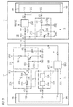
- Figure 2 shows a circuit diagram of a first example a part of the UART bus system of Figure 1 with two bus participants 3A, 3B.
- the bus subscriber 3B has a microcontroller 8B with UART bus interface 9B on.
- This UART bus interface 9B has a UART transmit output 10B and a UART receive input 11B on. Furthermore, an interrupt input 12B is provided. about the inputs 11B, 12B and the output 10B of the interface 9B is the microcontroller 8B with the single-wire bus line 4 coupled.
- the bus subscriber 3B also has a simple, commonly used transceivers 7B on.
- the bus interface 9A In contrast to the bus interface 9B is the bus interface 9A of the bus node 3A not as a UART interface educated.
- the bus interface 9A has a transmission output 10A, which is designed as an output compare output (TxD) is. Furthermore, an input 11A is provided, which serves as an input capture input (RxD) is formed. Finally one is further input 12A is provided, which serves as an interrupt input is trained. This interrupt input 12A is internally with connected to a Schmitt trigger circuit.
- the bus participant 3A also has a transceiver 7A.
- transceiver 7B The structure of the transceiver 7B will first be described below and then that of the transceiver 7A.
- the transceiver 7B has an input path 13B and a Output path 14B on.
- the input path 13B connects the inputs 11B, 12B with the single-wire bus line 4, whereas the Output path 14B the output 10B with the single-wire bus line. 4 combines.
- a circuit device 15B which is a protective element 16B, for example Resistor, upstream.
- the circuit device 15B is with supply connections for the first supply potential VBB and the second supply potential GND connected. Further, the circuit device 15B is connected to one terminal connected to a third supply potential VCC.
- the circuit device 15B is used for buffering an input side via the single-wire line 4 coupled bus signal X1.
- This bus signal X1 is in the circuit device 16B from a first supply voltage VBB-GND to a second supply voltage VCC-GND transformed down. For example, the supply voltage in the circuit device 15B lowered from 12V to 5V. That from the circuit means 15B provided on the output side Signal X2 is supplied to the two inputs 11B, 12B.
- the output path 14B has an output driver 21B.
- the Output driver 21B includes a transistor 17B which is over a transmission signal X3 provided by the output 10B is activated becomes. Between the output 10B and the control input of the transistor 17B is further a bias resistor 18B for adjustment of the tax potential.
- the transistor 17B generates on the output side a signal X4, which on the one hand via the one-wire bus power 4 is transmitted and on the other hand is fed back as an echo in the input path 13B.
- Parallel to the controlled path of the transistor 17B is a buffer capacitor 19B, parallel to the base-emitter terminals of transistor 17B, a resistor 20B.
- the transceiver 7A additionally a comparator 22A in the input path 13A on.
- the low pass filter 24A is for setting an appropriate delay due to different signal propagation times of the Signals in transmission path 13A and reception path 14A.
- the low pass filter 24A is the output side with the interrupt input 12A connected.
- the XOR gate 23A has two inputs, wherein a first input to the output of the circuit device 15A and the second input to the transmission output 10A of Interface 9A is connected. The XOR gate 23A thus becomes the output signal Y2 of the circuit device 15A and the output signal Y3 of the interface 9A supplied.
- a level converter 25A in the transmission path 14A is arranged.
- the level converter 25A includes a second one Transistor 26A, the control side via a resistor 27A is connected to the transmission output 10A.
- the transistor 26A is supplied via the supply potential VCC. Between the supply connection for the supply potential VCC and the control terminal of the transistor 26A is a resistor 28A is provided for setting a level. On the output side is the transistor 26A to the input of the output driver 21A connected.
- the operation of the transceiver 7A is short described. It is assumed that at a bus subscriber, the right to broadcast (dominant) is the data to be sent have a logical "zero" (LOW). That means alike that a logical "one" (HIGH) is a recessive state the one-wire bus line or a bus station called.
- the output driver 21A of the bus subscriber 3A is similar like the output driver 21B of the bus driver 3B, a driver transistor 17A, a series resistor 18A, a buffer capacitor 19A and a resistor 20A. Additionally points the output driver 21A has a resistor 29A acting as Pull-up resistor is formed and between the connection for the positive supply potential VBB and the Collector-side terminal of the driver transistor 17A arranged is. A tap between the collector side connection the driver transistor 17A and the pull-up resistor 29A forms the output of the driver stage 21A. This exit the driver stage 21A is connected to the input / output terminal 43A of the bus subscriber 3A.
- the transmission mode of the interface 9A is to be sent Date Y3 provided at the output 10A and the level converter 25A is converted into a signal Y4, the signal Y3 being inverted, ie sign is reversed.
- This signal Y4 is converted by the output driver 21A into a signal Y5, which is placed on the single-wire bus interface 4. That too Signal Y5 is inverted from signal Y4. At least a part Y1 of this transmitted signal Y5 is used as well Echo fed back to receive path 13A.
- the resulting from the switch means 15A converted and buffered signal Y2 is supplied to a first input of the XOR gate 23A.
- the second input of the XOR gate 23A becomes the one to be sent Signal Y3 supplied.
- the two signals Y2, Y3 at the input of the XOR gate 23A has a logical "zero". At the exit of the XOR gate 23A is therefore also a logical one "Zero" on.
- the comparator 22A thus recognizes that there is no short circuit or access collision and triggers no interrupt at input 12A.
- this diagnosis for an access collision or a short circuit on the single-wire bus line 4 can additionally or alternatively by a more or less elaborate software.
- the special advantage in the hardware implementation according to FIG 2, however, is that this hardware diagnosis a much higher data transfer rate and therefore one greater speed of data communication.
- FIG. 3 shows a data frame format for a data communication in a bus system according to the invention.
- a data frame 30 contains an example 2 byte wide "header" 31, a for example, 0 - 15 bytes wide date 32, in which the user data are included, as well as, for example, 2 bytes wide Field 33, in which a checksum to verify the sent Date 32 is included.
- the header 31 besides the Address also user-defined message type ID data and length field information.
- the header 31 thus contains in particular the address of a Busteil ceremonies, for which determines the data to be sent 32 are. For this reason, this address data is before the Transmission of the actual user data 32 to be sent transmitted. Based on this address data according to the invention In addition, it is checked whether an access collision exists. An access collision occurs when, at least two bus participants more or less simultaneously over the same Single-wire bus line want to send data. But there only one of these bus subscribers, namely or based on the Address data as dominant detected bus subscribers bus access receives, it must be prevented that the remaining bus participants at the same time data via its bus interface send. This procedure can thus be prioritized or arbitration be made. The arbitration is not here with the bus arbitration of a CANbas notorious Bus system to compare. Checking the bus access authorization is done here software or hardware as to which bus subscriber is dominant.
- Such an access request will be from another Bus participants also recognized as such.
- relatively rare Cases can happen, however, that several bus participants more or less simultaneously over the same single-wire bus data want to send. In these relatively rare cases it can come to an access collision. It therefore exists here special need such an access collision as possible to recognize quickly, i. preferably within the first bits or bytes of an address.
- a first byte of a data frame which, for example, in FIG the header 31 is provided, just for this bus subscriber distinctive and thus unique bit pattern on.
- This bit pattern can advantageously also be the address represent this bus participant.
- FIG. 4 shows the address format of a 1-byte-wide address field 34 of a bus participant.
- the address field 34 includes a first 4-bit wide address field 35 and a second 4-bit wide address field 36.
- the first address field (source address) 35 the address of the bus subscriber is stored, of which data is being sent
- the second address field (Destination address) 36 is the address of the bus user filed, to which the data should be sent.
- the addresses of a bus participant can be more or less arbitrary to get voted. However, they should each be unique and possibly as characteristic of just this bus subscriber be. Using these addresses, every bus user can the bus system to detect a bus access collision.
- Each bus user can have one of these addresses, being careful that one address each just forgiven. When using these addresses can in a very simple way an access collision of each Bus subscribers are detected.
- Figure 5 shows on the basis of three sub-figures (A) - (C) schematic Representations for comparing the addresses of different Bus subscriber to illustrate the invention Method for detecting an access collision.
- Figure 2 shows a circuit diagram of a first example a part of the UART bus system of Figure 1 with two Bus subscribers 3A, 3B.
- a respective address field 34 is preceded by a start bit 37, which typically has a logical "0".
- the start bit 37 indicates that subsequently an address and thus a data transfer begins.
- the address field 34 is a parity bit 38 and a stop bit 39 downstream.
- the Stop bit 39 which typically includes a logical "1", indicates an end of the address.
- FIGS. 5 (A) - 5 (C) are each two address fields 34 of bus subscribers, which submit an access request to the single-wire bus.
- the abbreviation for this access request x12 is used, which indicates that the bus participant with the address "1" on the bus subscriber with the address "2" Want to send data.
- FIG. 5 shows three examples (FIGS. 5 (A) - (C)) in which in each case the addresses according to FIG. 4 are used.
- the crosses designate bits due to an access collision have led to an echo, which triggers an interrupt. Since every bus user has its own specific address bits It can not come to the constellation, the only one bus user detects the access collision. Rather, this access collision is advantageously carried out by detected all bus users accessing the bus. The Situation that only one bus user an access collision detected can no longer occur.
- FIG. 6 shows a second example of part of the UART bus system from Figure 1, which with a Diagnoseeinrichting Is provided.
- the Pull-up resistor 29A designed as a switchable resistor.
- a controllable switch 40A arranged between the connection for the positive supply potential VBB and the pull-up resistor 29A.
- the controllable switch 40A is advantageously as a transistor, for example as a bipolar transistor, MOSFET, JFET, etc., trained.
- the control terminal of the controllable Switch 40A is connected to a control output 41A of the microcontroller 8A connected.
- the controllable switch 40A can be so act on the control output 41A with a control signal 42A.
- a high-impedance resistor for example, a pull-down resistor 44A arranged on the side of the bus participant 3B.
- a low-resistance resistor 45B arranged on the side of the bus participant 3B.
- this Diagnostic circuit 29A, 40A, 41A, 44A, 45B, 46A, 47A leaves a short circuit of the single wire bus 4 against the positive or the negative supply potential VBB, GND or a Detect idling of the bus line 4. Depending on present Error case is at the input / output terminal 43A a flat typical potential for this error case.
- One of this Potential-derived diagnostic signal is a diagnostic input 47A of the microcontroller 8A via a circuit device 46A feedable.
- the circuit device 46A is for Example equivalent to the circuit devices 15A, 15B built and serves the buffering and conversion of a in the Circuit device 46A input-side coupled signal.
- FIG. 7 shows a block diagram on the basis of which the invention Diagnostic method is explained in more detail, which in a Bus subscriber is performed according to Figure 6.
- the bus subscriber 3A has a diagnostic device on, via the one-wire bus 4 and a communicating with the bus subscriber 3A via this single-wire bus line 4 further bus participant 3B diagnosable are.
- a diagnostic mode for diagnosing the further bus subscriber 3B and the single-wire bus line 4 intended.
- Diagnostic signal 48A has a high logic level (HIGH, "1") on, then there is a short circuit of the single-wire bus line 4 with the positive supply potential VBB (53). Does that know On the other hand, the diagnostic signal 48A has a low logic level on, then the controllable switch 40A becomes the control signal 42A is turned on (54). Subsequently, the Potential of the diagnostic signal injected into diagnostic input 47A 48A checked (55). Indicates this diagnostic signal 48A has a low logic level, then there is a short circuit the single wire bus line 4 with the potential of the reference ground GND before. In the other case, that is at a high logic level of the diagnostic signal 48A, is idle the single-wire bus line 4 (open or interrupted single-wire bus line) before (57).
- an echo signal Y1 is received (51), then first checks whether the echo signal Y1 with the respectively sent Signal Y3 correlates, that is, whether there is an echo error (58). If there is a wrong or erroneous echo signal Y1, then can be closed to a disturbance of the single-wire bus line 4 become (59).
- the disorder can be caused, for example, by overlapping from interfering signals or from a collision of several Bus participants 3B - 3D result on the same single-wire bus line 4. Is the echo signal Y1 correct with the transmitted signal Y3 match, first checks whether the other bus participants 3B has sent a response signal X4 (60).
- the method assumes that resistor 44A dimensioned much larger than the resistor 45B. Due to this different dimensioning of the two resistors 44A, 45B may be as needed in diagnostic mode such potentials are tapped at the input / output port 43A which provide the various diagnostic signals 48A, which are each characteristic of the corresponding Error case.
- diagnostic mode by this measure the quiescent current, which is between the two Bus subscribers 3A, 3B flows over the single-wire bus line 4, significantly reduced, which on the one hand lower power consumption and on the other hand, a lower burden on electronic components of these bus participants 3A, 3B causes.
- the invention is not necessarily to a UART bus system limited, but goes without saying extend to any single-wire bus systems.
- bus interfaces and transceivers are not necessarily on the in the present embodiment limited structure shown. Rather, the better Presentation of the invention, in particular with regard to the embodiment the transceiver deliberately a circuit technology very simple construction chosen. Of course you can here also depending on the desired application and application provide more complex transceiver circuits. In particular, the transceivers typically are in the receive path much more sophisticated protection elements and buffer circuits on. Also, as driver circuits arbitrary other drivers, such as tristate drivers, push-pull output stages, Differential amplifier or the like used become.
- This review and definition does not necessarily have to be based on an address field or the addresses of the various Bus participants take place. Rather, it can be very beneficial here an arbitrary data field can be used, which is a corresponding function code or an identification code which has a more or less unique identification the respective addressee. About this identification Each bus participant can determine which other Bus participants still want to access the bus.
Landscapes
- Engineering & Computer Science (AREA)
- Computer Networks & Wireless Communication (AREA)
- Signal Processing (AREA)
- Small-Scale Networks (AREA)
Abstract
Description
- Figur 1
- ein verallgemeinertes Blockschalbild für ein UART-Bussystem;
- Figur 2
- ein erstes Beispiel eines Teils des UART-Bussystems aus Figur 1, bei dem ein Busteilnehmer eine UART-Schnittstelle und der andere Busteilnehmer keine UART-Schnittstelle aufweist;
- Figur 3
- das Datenrahmenformat für eine Datenkommunikation;
- Figur 4
- das Adressformat des erfindungsgemäßen Protokolls;
- Figur 5
- schematische Darstellungen für den Vergleich der Adressbits unterschiedlicher Busteilnehmer zur Veranschaulichung des erfindungsgemäßen Verfahrens für eine Zugriffskollision über die Eindrahtbusleitung;
- Figur 6
- ein zweites Beispiel eines Teils des UART-Bussystems aus Figur 1, welches mit einer Diagnoseeinrichting ausgestattet ist;
- Figur 7
- ein Blockschaltbild, anhand dem das erfindungsgemäße Diagnoseverfahren einer Diagnoseeinrichtung entsprechend Figur 6 näher erläutert wird.
- 1
- (UART-)Bussystem
- 2
- Bus
- 3A - 3D
- Busteilnehmer, Knoten
- 4
- (Eindraht-)Busleitung
- 5
- Versorgungsleitung
- 6
- Versorgungsleitung
- 7A - 7D
- Transceiver
- 8A - 8D
- Mikrocontroller
- 9A - 9D
- (Bus-)Schnittstellen
- 10A, 10B
- Sendeausgang
- 11A, 11B
- Empfangseingang
- 12A, 12B
- Interupt-Eingang
- 13A, 13B
- Empfangspfad
- 14A, 14B
- Sendepfad
- 15A, 15B
- Schaltungseinrichtung
- 16A, 16B
- Schutzelement
- 17A, 17B
- Treibertransistor
- 18A, 18B
- Vorwiderstand
- 19A, 19B
- Pufferkondensator
- 20A, 20B
- Widerstand
- 21A, 21B
- Ausgangstreiber
- 22A
- Vergleicherschaltung
- 23A
- XOR-Gatter
- 24A
- Tiefpassfilter
- 25A
- Pegelwandler
- 26A
- Pegelwandlertransistor
- 27A
- Vorwiderstand
- 28A
- Widerstand
- 29A
- (pull-up-)Widerstand
- 30
- Datenrahmenformat
- 31
- Header
- 32
- Datenfeld
- 33
- Feld für Prüfsumme
- 34
- Adressfeld
- 35
- erster Teil des Adressfelds
- 36
- zweiter Teil des Adressfelds
- 37
- Start-Bit
- 38
- Parity-Bit
- 39
- Stopp-Bit
- 40A
- steuerbarer Schalter, MOSFET
- 41A
- Steuerausgang
- 42A
- Steuersignal
- 43A, 43B
- Eingangs/Ausgangsanschlüsse
- 44A
- (hochohmiger) Widerstand
- 45B
- (niederohmiger) Widerstand
- 46A
- Schaltungseinrichtung
- 47A
- Diagnoseeingang
- 48A
- Diagnosesignal
- 50 - 62
- Verfahrensschritte
- VBB
- (erstes, positives) Versorgungspotenzial
- GND
- (zweites) Versorgungspotenzial, Bezugspotenzial
- VCC
- Versorgungspotenzial
- X1, X2
- Empfangssignale
- X3, X4
- Sendesignale
- Y1, Y2
- Empfangssignale
- Y3 - Y5
- Sendesignale
- Y6
- Interuptsignal
Claims (28)
- Schnittstellenschaltung zur Ankopplung eines über einen UART-basiertes Bussystem (1) anzusprechenden Busteilnehmers (3A) an einen Eindrahtbus (4) des Bussystems (1),
mit einem Datenausgang (10A) zum Ausgeben eines über den Eindrahtbus zu sendenden, binären ersten Datensignals (Y3),
mit einem Dateneingang (11A) zum Aufnehmen eines binären zweiten Datensignals (Y2), welches von über den Eindrahtbus (4) empfangenen Datensignalen (Y1) und/oder von dem ersten Datensignal (Y2) abgeleiteten Echosignals (Y1) abgeleitet ist,
mit einer als Hardwareschaltung ausgebildeten Vergleichereinrichtung (22A), die aus einem Vergleich der eingangsseitig eingekoppelten ersten und zweiten Datensignale (Y2, Y3) einen Zugriffskonflikt mehreren auf den Eindrahtbus zugreifenden Busteilnehmer (3A - 3D) und/oder einen Kurzschluss des Eindrahtbus (4) erkennt und die in diesem Falle ein Interuptsignal (Y6) ausgibt,
mit einem Interupteingang (12A) zum Aufnehmen des Interuptsignals (Y6). - Schnittstellenschaltung nach Anspruch 1,
dadurch gekennzeichnet, dass die Vergleichereinrichtung (22A) ein XOR-Gatter (23A) aufweist, die die ersten und zweiten binären Datensignale (Y2, Y3) bitweise miteinander vergleicht. - Schnittstellenschaltung nach Anspruch 2,
dadurch gekennzeichnet, dass die Vergleichereinrichtung (22A) ein dem ODER-Gatter (23A) nachgeschaltete Tiefpassfilter (24A) aufweist, welches eine Verzögerung aufgrund von unterschiedlichen Signallaufzeiten des ersten und des zweiten Datensignals (Y2, Y3) einstellt. - Schnittstellenschaltung nach einem der vorstehenden Ansprüche,
dadurch gekennzeichnet, dass in einem Datenrahmenformat (30) der Datensignale jeweils ein Identifikationsfeld (34) vorgesehen ist, welches eine eindeutige Identifikation der Busteilnehmer (3A - 3D) ermöglicht. - Schnittstellenschaltung nach Anspruch 4,
dadurch gekennzeichnet, dass das Identifikationsfeld (34) als Adressfeld (34) ausgebildet ist, welches die Quelladresse (35) und die Zieladresse (36) eines zu sendenden Datensignals (Y3) enthält, wobei die Vergleichereinrichtung (22A) dazu ausgelegt ist, lediglich die Bits der Adressfelder (34) des ersten und des zweiten Datensignals (Y2, Y3) bitweise miteinander zu vergleichen. - Schnittstellenschaltung nach einem der vorstehenden Ansprüche,
dadurch gekennzeichnet, dass der Dateneingang (11A) als Input-Capture-Eingang und der Datenausgang (10A) als Capture-Compare-Ausgang ausgebildet ist. - Schnittstellenschaltung nach einem der vorstehenden Ansprüche,
dadurch gekennzeichnet, dass eine Interupteinrichtung, die einen Interupteingang (12A) zur Einkopplung des Interuptsignal (Y6) aufweist und die bei Vorliegen des Interuptsignals (Y6) eine Datenkommunikation des Busteilnehmers (3A) zu zumindest einem weiteren Busteilnehmer (3B - 3D) unterbricht oder stoppt. - Schnittstellenschaltung nach einem der vorstehenden Ansprüche,
dadurch gekennzeichnet, dass die Schnittstellenschaltung einen zwischen dem Dateneingang (11A) und dem Datenausgang (10A) einerseits und dem Eindrahtbus (4) andererseits angeordneten Transceiver (7A) aufweist, wobei der Transceiver (7A) einen Sendepfad (14A), in dem ein Ausgangstreiber (21A) angeordnet ist, und einen Empfangspfad (13A) aufweist. - Schnittstellenschaltung nach Anspruch 8,
dadurch gekennzeichnet, dass im Empfangspfad (13A) eine Pufferschaltung (15A) zur Pufferung eines eingangsseitig über den Eindrahtbus (4) eingekoppeltes erstes Datensignals (Y1) vorgesehen ist. - Schnittstellenschaltung nach einem der Ansprüche 8 oder 9,
dadurch gekennzeichnet, dass im Empfangspfad (13A) eine Spannungswandlerschaltung (15A) vorgesehen ist, die ein über den Eindrahtbus (4) eingekoppeltes erstes Datensignal (Y1) von einer ersten Versorgungsspannung (VBB-GND) auf eine zweite Versorgungsspannung (VCC-GND) herunter transformiert. - Schnittstellenschaltung nach einem der Ansprüche 8 bis 10,
dadurch gekennzeichnet, dass im Sendepfad (14A) ein Pegelwandler (25A) zur Wandlung des Pegels des zu sendenden ersten Datensignals (Y3) vorgesehen ist. - Schnittstellenschaltung nach einem der vorstehenden Ansprüche,
dadurch gekennzeichnet, dass die Schnittstellenschaltung zumindest einen weiteren Dateneingang, der als UART-Eingang ausgebildet ist, und zumindest einen weiteren Datenausgang, der als UART-Ausgang ausgebildet ist, aufweist. - Schnittstellenschaltung nach einem der vorstehenden Ansprüche,
dadurch gekennzeichnet, dass eine Diagnoseeinrichtung (29A, 40A, 41A, 44A - 47A) zur Diagnose des Zustands der Eindrahtbusses (4) und/oder zumindest eines weiteren mit dem Busteilnehmer (3B) über die Schnittstellenschaltung kommunizierenden Busteilnehmers (3B - 3D) vorgesehen ist, wobei die Elemente der Diagnoseeinrichtung (29A, 40A, 41A, 44A - 47A) über einen Eingangs/Ausgangsanschluss (43A) jeweils mit dem Eindrahtbusses (4) gekoppelt sind. - Schnittstellenschaltung Anspruch 13,
dadurch gekennzeichnet, dass die Diagnoseeinrichtung (29A, 40A, 41A, 44A - 47A) einen mit einem Versorgungspotenzial (VBB, GND) verbindbaren ersten Widerstand (29A) enthält. - Schnittstellenschaltung nach einem der Ansprüche 13 oder 14,
dadurch gekennzeichnet, dass die Diagnoseeinrichtung (29A, 40A, 41A, 44A - 47A) einen steuerbaren Schalter (40A) aufweist, dessen Lastpfad zwischen dem ersten Widerstand (29A) und dem positiven Versorgungspotenzial (VBB) angeordnet ist und dessen Steueranschluss zur Ansteuerung mit einem Steuersignal (42A) mit einem Steueranschluss (41A) gekoppelt ist. - Schnittstellenschaltung nach einem der Ansprüche 13 - 15,
dadurch gekennzeichnet, dass die Diagnoseeinrichtung (29A, 40A, 41A, 44A - 47A) einen zweiten Widerstand (44A) aufweist, der zwischen dem Eingangs/Ausgangsanschluss (43A) und einem Anschluss für ein negatives Versorgungspotenzial oder ein Bezugspotenzial (GND) angeordnet ist. - Schnittstellenschaltung nach einem der Ansprüche 13 - 16,
dadurch gekennzeichnet, dass die Diagnoseeinrichtung (29A, 40A, 41A, 44A - 47A) einen Diagnoseingang (47A) aufweist, der mit dem Eingangs/Ausgangsanschluss (43A) verbunden ist und in den in einem Diagnosebetrieb somit ein am Eingangs/Ausgangsanschluss (43A) abgreifbares Diagnoseeingangssignal (48) einkoppelbar ist. - Bussystem (1)
mit einem UART-basierten Eindrahtbus (4),
mit einer Vielzahl von Busteilnehmern (3A - 3D), wobei ein Busteilnehmer (3A - 3D) jeweils
zumindest eine Transceiverschaltung (7A - 7D), die die physikalische Anbindung an den Eindrahtbus (4) gewährleistet,
zumindest eine über den Eindrahtbus (4) anzusprechende Einrichtung (8A - 8D), die die Daten verarbeitet und die Datenkommunikation steuert, und
zumindest eine Schnittstellenschaltung (9A - 9D), über die die Datenkommunikation über den Eindrahtbus (4) nach Maßgabe eines Busprotokolls erfolgt, aufweist,
wobei zumindest ein Busteilnehmer (3A) eine Schnittstellenschaltung (9A, 7A) nach einem der vorstehenden Ansprüche aufweist. - Bussystem nach Anspruch 18,
dadurch gekennzeichnet, dass zumindest ein Busteilnehmer (3B - 3D) eine Schnittstellenschaltung (9B - 9D) aufweist, die zumindest einen UART-Eingang (11B) und zumindest einen UART-Ausgang (10B) aufweist. - Bussystem nach einem der Ansprüche 18 oder 19,
dadurch gekennzeichnet, dass zumindest eine Einrichtung (8A - 8D) als programmgesteuerte Einrichtung, insbesondere als Mikroprozessor oder als Mikrocontroller, ausgebildet ist. - Bussystem nach einem der Ansprüche 18 bis 20,
dadurch gekennzeichnet, dass zumindest eine Schnittstellenschaltung (9A - 9D) als Hardwareschnittstelle ausgebildet ist. - Bussystem nach einem der Ansprüche 18 bis 21,
dadurch gekennzeichnet, dass jeder Busteilnehmer (3A - 3D) eine für diesen Busteilnehmer (3A - 3D) charakteristische Adresse aufweist. - Verfahren zum Betreiben einer Schnittstellenschaltung nach einem der Ansprüche 1 bis 17,
dadurch gekennzeichnet, dass in einem Datenrahmenformat der Datensignale jeweils ein Identifikationsfeld (34) vorgesehen ist, welches eine eindeutige Identifikation der Busteilnehmer (3A - 3D) ermöglicht. - Verfahren nach Anspruch 23,
dadurch gekennzeichnet, dass das Identifikationsfeld (34) als Adressfeld (34) ausgebildet ist, welches die Quelladresse (35) und Zieladresse (36) eines gesendeten Datensignals enthält, wobei lediglich die Bits der Adressfelder (34) des ersten und des zweiten Datensignals (Y2, Y3) bitweise miteinander verglichen werden. - Verfahren nach einem der Ansprüche 23 oder 24,
dadurch gekennzeichnet, dass in einem Datenrahmenformat der Datensignale (Y2, Y3) jeweils ein Datenfeld (32) für die zu übertragenden Nutzdaten vorgesehen ist, wobei der Vergleich der Adressfelder (31, 34) stattfindet, noch bevor die eigentlichen Daten in dem Datenfeld (32) übertragen werden. - Verfahren nach einem der Ansprüche 24 oder 25,
dadurch gekennzeichnet, dass jeder Busteilnehmer (3A - 3D) eine für diesen Busteilnehmer (3A - 3D) charakteristische Identifikation aufweist. - Verfahren zum Betreiben einer Schnittstellenschaltung nach einem der Ansprüche 1 bis 17,
dadurch gekennzeichnet, dass ein Diagnosebetrieb (50 - 62) vorgesehen ist, bei dem im Falle, dass kein Echosignal (Y1) auf ein gesendetes Signal (Y3) hin empfangen wird, folgende Verfahrensschritte vorgenommen werden:Überprüfen (52) des Potenzials des am Eingangs/Ausgangsanschluss (43A) anliegenden Diagnosesignals (48A);Einschalten (54) des steuerbaren Schalters (40A);Erneutes Überprüfen (55) des Potenzials des Diagnosesignals (48A). - Verfahren nach Anspruch 27,
dadurch gekennzeichnet, dass im Falle, dass kein Echosignal (Y1) auf ein gesendetes Signal (Y3) hin empfangen wird, folgende Verfahrensschritte im Diagnosebetrieb (50 - 62) vorgenommen werden:Überprüfen (58), ob das empfangene Echosignal (Y1) dem gesendeten Signal (Y3) entspricht;Überprüfen (60) eines Antwortsignals (X4) eines über den Eindrahtbus (4) mit der Schnittstellenschaltung kommunizierenden weiteren Busteilnehmers (3B).
Applications Claiming Priority (4)
| Application Number | Priority Date | Filing Date | Title |
|---|---|---|---|
| DE2003140806 DE10340806B3 (de) | 2003-09-04 | 2003-09-04 | Schnittstelle für ein UART-basiertes Bussystem |
| DE10340806 | 2003-09-04 | ||
| DE10358039 | 2003-12-11 | ||
| DE10358039 | 2003-12-11 |
Publications (2)
| Publication Number | Publication Date |
|---|---|
| EP1515237A1 true EP1515237A1 (de) | 2005-03-16 |
| EP1515237B1 EP1515237B1 (de) | 2007-02-21 |
Family
ID=34137324
Family Applications (1)
| Application Number | Title | Priority Date | Filing Date |
|---|---|---|---|
| EP20040103833 Expired - Lifetime EP1515237B1 (de) | 2003-09-04 | 2004-08-09 | Schnittstelle für ein UART-basiertes Bussystem |
Country Status (2)
| Country | Link |
|---|---|
| EP (1) | EP1515237B1 (de) |
| DE (1) | DE502004002939D1 (de) |
Cited By (1)
| Publication number | Priority date | Publication date | Assignee | Title |
|---|---|---|---|---|
| CN114676078A (zh) * | 2022-03-25 | 2022-06-28 | 惠州高盛达智显科技有限公司 | 一种基于uart接口信号的自动识别方法 |
Citations (6)
| Publication number | Priority date | Publication date | Assignee | Title |
|---|---|---|---|---|
| US4063220A (en) * | 1975-03-31 | 1977-12-13 | Xerox Corporation | Multipoint data communication system with collision detection |
| US4259663A (en) * | 1979-06-07 | 1981-03-31 | Ford Motor Company | Contention interference detection by comparison of transmitted and received signal information |
| EP0246666A2 (de) * | 1986-05-22 | 1987-11-25 | Chrysler Corporation | Serieller Datenbus für verschiedene Betriebsarten (SCI, SPI und gepufferte SPI) und Verfahren für serielle Peripherieschnittstelle in einem seriellen Datenbus |
| US5636343A (en) * | 1995-01-31 | 1997-06-03 | Mitsubishi Electric Semiconductor Software Co., Ltd. | Microcomputer with built-in serial input-output circuit and collision detection circuit responsive to common input-output line being occupied |
| EP0952706A2 (de) * | 1998-04-17 | 1999-10-27 | Ford Global Technologies, Inc. | Vehfaren zur Entdeckung und Lösung von Datenkorruption in einem UART-basierten Kommunikationsnetzwerk |
| DE10045947A1 (de) * | 2000-09-22 | 2002-04-11 | Thees Joachim | Vorrichtung und Verfahren zur Kommunikation zwischen Microcontrollern |
-
2004
- 2004-08-09 DE DE200450002939 patent/DE502004002939D1/de not_active Expired - Lifetime
- 2004-08-09 EP EP20040103833 patent/EP1515237B1/de not_active Expired - Lifetime
Patent Citations (6)
| Publication number | Priority date | Publication date | Assignee | Title |
|---|---|---|---|---|
| US4063220A (en) * | 1975-03-31 | 1977-12-13 | Xerox Corporation | Multipoint data communication system with collision detection |
| US4259663A (en) * | 1979-06-07 | 1981-03-31 | Ford Motor Company | Contention interference detection by comparison of transmitted and received signal information |
| EP0246666A2 (de) * | 1986-05-22 | 1987-11-25 | Chrysler Corporation | Serieller Datenbus für verschiedene Betriebsarten (SCI, SPI und gepufferte SPI) und Verfahren für serielle Peripherieschnittstelle in einem seriellen Datenbus |
| US5636343A (en) * | 1995-01-31 | 1997-06-03 | Mitsubishi Electric Semiconductor Software Co., Ltd. | Microcomputer with built-in serial input-output circuit and collision detection circuit responsive to common input-output line being occupied |
| EP0952706A2 (de) * | 1998-04-17 | 1999-10-27 | Ford Global Technologies, Inc. | Vehfaren zur Entdeckung und Lösung von Datenkorruption in einem UART-basierten Kommunikationsnetzwerk |
| DE10045947A1 (de) * | 2000-09-22 | 2002-04-11 | Thees Joachim | Vorrichtung und Verfahren zur Kommunikation zwischen Microcontrollern |
Cited By (1)
| Publication number | Priority date | Publication date | Assignee | Title |
|---|---|---|---|---|
| CN114676078A (zh) * | 2022-03-25 | 2022-06-28 | 惠州高盛达智显科技有限公司 | 一种基于uart接口信号的自动识别方法 |
Also Published As
| Publication number | Publication date |
|---|---|
| EP1515237B1 (de) | 2007-02-21 |
| DE502004002939D1 (de) | 2007-04-05 |
Similar Documents
| Publication | Publication Date | Title |
|---|---|---|
| DE69433882T2 (de) | Vorrichtung zur Übertragung von Daten | |
| EP0658258B1 (de) | Netzwerkschnittstelle | |
| EP3977682B1 (de) | Fehlererkennung-testeinrichtung für eine teilnehmerstation eines seriellen bussystems und verfahren zum testen von mechanismen zur fehlererkennung bei einer kommunikation in einem seriellen bussystem | |
| EP1198736A1 (de) | Verfahren zum konfigurieren eines feldbus-teilnehmers | |
| EP3725041B1 (de) | Verfahren zur bereitstellung von informationen für die lokalisierung von fehlern in einem kommunikationsnetzwerk eines gerätes, entsprechend ausgelegte busteilnehmerstation sowie fahrzeug | |
| DE102018221957A1 (de) | Einrichtung für eine Teilnehmerstation eines seriellen Bussystems und Verfahren zur Kommunikation in einem seriellen Bussystem | |
| EP3977683B1 (de) | Einrichtung für eine teilnehmerstation eines seriellen bussystems und verfahren zur kommunikation in einem seriellen bussystem | |
| EP3970324B1 (de) | Sende-/empfangseinrichtung und kommunikationssteuereinrichtung für eine teilnehmerstation eines seriellen bussystems und verfahren zur kommunikation in einem seriellen bussystem | |
| WO2020120555A1 (de) | Teilnehmerstation für ein serielles bussystem und verfahren zur kommunikation in einem seriellen bussystem | |
| DE10340806B3 (de) | Schnittstelle für ein UART-basiertes Bussystem | |
| WO2021058432A1 (de) | Konfliktdetektor für eine teilnehmerstation eines seriellen bussystems und verfahren zur kommunikation in einem seriellen bussystem | |
| WO2020126754A1 (de) | Einrichtung für eine teilnehmerstation eines seriellen bussystems und verfahren zur kommunikation in einem seriellen bussystem | |
| EP1515237B1 (de) | Schnittstelle für ein UART-basiertes Bussystem | |
| EP4094407B1 (de) | Sende-/empfangseinrichtung und kommunikationssteuereinrichtung für eine teilnehmerstation eines seriellen bussystems und verfahren zur kommunikation in einem seriellen bussystem | |
| WO2021148351A1 (de) | Sende-/empfangseinrichtung und kommunikationssteuereinrichtung für eine teilnehmerstation eines seriellen bussystems und verfahren zur kommunikation in einem seriellen bussystem | |
| WO2022017820A1 (de) | Einrichtungen für eine teilnehmerstation eines seriellen bussystems und verfahren zur kommunikation in einem seriellen bussystem | |
| DE10243319B4 (de) | Sichere Datenübertragung | |
| WO2021047894A1 (de) | Einrichtung für eine teilnehmerstation eines seriellen bussystems und verfahren zur kommunikation in einem seriellen bussystem | |
| DE102019212033A1 (de) | Teilnehmerstation für ein serielles Bussystem und Verfahren zur Kommunikation in einem seriellen Bussystem | |
| EP3681109B1 (de) | Verfahren zum erkennen eines zustands eines teilnehmers eines kommunikationsbusses, kommunikationsbussystem, verriegelungsanlage mit einem kommunikationsbussystem und transceiver | |
| WO2021148348A1 (de) | Sende-/empfangseinrichtung für eine teilnehmerstation eines seriellen bussystems und verfahren zur kommunikation in einem seriellen bussystem | |
| WO2020244986A1 (de) | Teilnehmerstation für ein serielles bussystem und verfahren zur kommunikation in einem seriellen bussystem | |
| EP4094408A1 (de) | Sende-/empfangseinrichtung und kommunikationssteuereinrichtung für eine teilnehmerstation eines seriellen bussystems und verfahren zur kommunikation in einem seriellen bussystem | |
| WO2020109313A1 (de) | Teilnehmerstationen für ein serielles bussystem und verfahren zum übertragen einer nachricht in einem seriellen bussystem | |
| DE102024206781A1 (de) | Sende-/Empfangseinrichtung für eine Teilnehmerstation eines seriellen Bussystems und Verfahren zur Kommunikation mit differentiellen Signalen in einem seriellen Bussystem |
Legal Events
| Date | Code | Title | Description |
|---|---|---|---|
| PUAI | Public reference made under article 153(3) epc to a published international application that has entered the european phase |
Free format text: ORIGINAL CODE: 0009012 |
|
| AK | Designated contracting states |
Kind code of ref document: A1 Designated state(s): AT BE BG CH CY CZ DE DK EE ES FI FR GB GR HU IE IT LI LU MC NL PL PT RO SE SI SK TR |
|
| AX | Request for extension of the european patent |
Extension state: AL HR LT LV MK |
|
| 17P | Request for examination filed |
Effective date: 20050217 |
|
| AKX | Designation fees paid |
Designated state(s): DE FR GB |
|
| GRAP | Despatch of communication of intention to grant a patent |
Free format text: ORIGINAL CODE: EPIDOSNIGR1 |
|
| GRAS | Grant fee paid |
Free format text: ORIGINAL CODE: EPIDOSNIGR3 |
|
| GRAA | (expected) grant |
Free format text: ORIGINAL CODE: 0009210 |
|
| AK | Designated contracting states |
Kind code of ref document: B1 Designated state(s): DE FR GB |
|
| REG | Reference to a national code |
Ref country code: GB Ref legal event code: FG4D Free format text: NOT ENGLISH |
|
| GBT | Gb: translation of ep patent filed (gb section 77(6)(a)/1977) |
Effective date: 20070221 |
|
| REF | Corresponds to: |
Ref document number: 502004002939 Country of ref document: DE Date of ref document: 20070405 Kind code of ref document: P |
|
| ET | Fr: translation filed | ||
| PLBE | No opposition filed within time limit |
Free format text: ORIGINAL CODE: 0009261 |
|
| STAA | Information on the status of an ep patent application or granted ep patent |
Free format text: STATUS: NO OPPOSITION FILED WITHIN TIME LIMIT |
|
| 26N | No opposition filed |
Effective date: 20071122 |
|
| REG | Reference to a national code |
Ref country code: FR Ref legal event code: TP |
|
| REG | Reference to a national code |
Ref country code: GB Ref legal event code: 732E Free format text: REGISTERED BETWEEN 20110825 AND 20110831 |
|
| PGFP | Annual fee paid to national office [announced via postgrant information from national office to epo] |
Ref country code: GB Payment date: 20120821 Year of fee payment: 9 |
|
| PGFP | Annual fee paid to national office [announced via postgrant information from national office to epo] |
Ref country code: FR Payment date: 20120906 Year of fee payment: 9 Ref country code: DE Payment date: 20120831 Year of fee payment: 9 |
|
| GBPC | Gb: european patent ceased through non-payment of renewal fee |
Effective date: 20130809 |
|
| PG25 | Lapsed in a contracting state [announced via postgrant information from national office to epo] |
Ref country code: DE Free format text: LAPSE BECAUSE OF NON-PAYMENT OF DUE FEES Effective date: 20140301 |
|
| REG | Reference to a national code |
Ref country code: DE Ref legal event code: R119 Ref document number: 502004002939 Country of ref document: DE Effective date: 20140301 |
|
| REG | Reference to a national code |
Ref country code: FR Ref legal event code: ST Effective date: 20140430 |
|
| PG25 | Lapsed in a contracting state [announced via postgrant information from national office to epo] |
Ref country code: GB Free format text: LAPSE BECAUSE OF NON-PAYMENT OF DUE FEES Effective date: 20130809 |
|
| PG25 | Lapsed in a contracting state [announced via postgrant information from national office to epo] |
Ref country code: FR Free format text: LAPSE BECAUSE OF NON-PAYMENT OF DUE FEES Effective date: 20130902 |