EP1515145A1 - Hochspannung-schnittstellenmodul - Google Patents
Hochspannung-schnittstellenmodul Download PDFInfo
- Publication number
- EP1515145A1 EP1515145A1 EP04021302A EP04021302A EP1515145A1 EP 1515145 A1 EP1515145 A1 EP 1515145A1 EP 04021302 A EP04021302 A EP 04021302A EP 04021302 A EP04021302 A EP 04021302A EP 1515145 A1 EP1515145 A1 EP 1515145A1
- Authority
- EP
- European Patent Office
- Prior art keywords
- voltage
- circuit
- resistance
- conditioning circuit
- reduced
- Prior art date
- Legal status (The legal status is an assumption and is not a legal conclusion. Google has not performed a legal analysis and makes no representation as to the accuracy of the status listed.)
- Withdrawn
Links
- 230000003750 conditioning effect Effects 0.000 claims abstract description 36
- 238000005070 sampling Methods 0.000 claims abstract description 17
- 238000012360 testing method Methods 0.000 claims abstract description 8
- 238000000034 method Methods 0.000 claims description 10
- 230000037361 pathway Effects 0.000 claims description 9
- 239000004593 Epoxy Substances 0.000 claims description 4
- 230000015556 catabolic process Effects 0.000 claims description 4
- 230000008878 coupling Effects 0.000 claims 1
- 238000010168 coupling process Methods 0.000 claims 1
- 238000005859 coupling reaction Methods 0.000 claims 1
- 238000005259 measurement Methods 0.000 description 8
- 230000035939 shock Effects 0.000 description 6
- 230000006378 damage Effects 0.000 description 3
- 238000013480 data collection Methods 0.000 description 2
- RYGMFSIKBFXOCR-UHFFFAOYSA-N Copper Chemical compound [Cu] RYGMFSIKBFXOCR-UHFFFAOYSA-N 0.000 description 1
- 230000004075 alteration Effects 0.000 description 1
- 239000000969 carrier Substances 0.000 description 1
- 230000001143 conditioned effect Effects 0.000 description 1
- 229910052802 copper Inorganic materials 0.000 description 1
- 239000010949 copper Substances 0.000 description 1
- 239000012212 insulator Substances 0.000 description 1
- 238000006467 substitution reaction Methods 0.000 description 1
Images


Classifications
-
- G—PHYSICS
- G01—MEASURING; TESTING
- G01R—MEASURING ELECTRIC VARIABLES; MEASURING MAGNETIC VARIABLES
- G01R15/00—Details of measuring arrangements of the types provided for in groups G01R17/00 - G01R29/00, G01R33/00 - G01R33/26 or G01R35/00
- G01R15/04—Voltage dividers
-
- G—PHYSICS
- G01—MEASURING; TESTING
- G01R—MEASURING ELECTRIC VARIABLES; MEASURING MAGNETIC VARIABLES
- G01R15/00—Details of measuring arrangements of the types provided for in groups G01R17/00 - G01R29/00, G01R33/00 - G01R33/26 or G01R35/00
- G01R15/14—Adaptations providing voltage or current isolation, e.g. for high-voltage or high-current networks
Definitions
- the present invention relates generally to voltage measurement systems and more particularly, a fail-safe system to measure unsafe voltages remotely by locally conditioning the measured voltages.
- a typical solution reduces unsafe voltage with a voltage divider or resistor network.
- a voltage divider or resistor network Such a circuit is shown in FIGURE 1.
- an unsafe voltage input 12 is applied to conditioning circuit 10.
- resistor 14 and resistor 16 divide or reduce the unsafe input voltage and provide a reduced output voltage 18 as described by Equation 1:
- Vout Vin R 16 ( R 14 + R 16 ) Equation 1 shows the ratio by which the unsafe voltage is reduced.
- the unsafe voltage is reduced by the ratio of resistor 16 to the sum of resistor 16 and resistor 14.
- output voltage 18 is significantly less than the unsafe input voltage 12.
- this simply solution has serious drawbacks. If resister 14 fails in a short circuit condition, output voltage 18 fails to equal voltage of unsafe input voltage 12.
- the present invention provides a high voltage interface system and method that substantially eliminates or reduces disadvantages and problems associated with previously developed voltage sampling methods used to measure unsafe voltages. More specifically, the present invention provides a voltage conditioning interface module to condition an electrical signal locally. This module receives the unsafe electrical signal at an input port. This input port is electrically coupled to an external sampling point on an electrical circuit or system under test.
- a conditioning circuit having both a voltage reducing circuit and a voltage limiting circuit provides a reduced voltage.
- the voltage limiting circuit is in parallel with the output terminals that output the reduced voltage. This arrangement ensures that when a circuit element within the voltage reducing circuit fails, an unsafe condition does not exist across these terminals.
- a first electrical pathway couples the received electrical signal to the conditioning circuit. This pathway typically employs high voltage carriers or leads.
- a second circuit pathway couples the modules output to a data acquisition or display.
- the voltage reducing circuit drops the unsafe voltage across a first resistance and a second resistance arranged in series.
- the output terminals measure the voltage drop across the second resistance.
- the voltage limiting circuit typically uses a transorb arranged in parallel to the second resistance.
- the voltage limiting circuit uses a first diode aligned such that if a voltage across the output terminals exceeds the diodes breakdown voltage, the output terminals are shunted to a reference point.
- a second diode in the circuit is arranged in parallel to the first diode, but aligned such that forward current flow in the second diode is opposite that of the first diode. This arrangement ensures that should the second resistance fail as an open circuit, the output terminals are shunted to ground.
- the voltage limiting circuit guarantees that a single point failure in either the first resistance or the second resistance does not result in the reduced voltage output exceeding a predetermined safe voltage.
- the voltage conditioning circuit may be encapsulated within an epoxy package.
- sampling point(s) within a circuit under test couple via a first circuit pathway to provide the sampled unsafe-voltage signal to a voltage divider circuit.
- This sampling point may be located within a complex system having a plurality of sampling points coupled to a remote data acquisition system.
- the sampled voltage drops across the voltage divider circuit.
- a reduced voltage measured across a portion of the voltage divider provides the reduced voltage output.
- the reduced voltage at the reduced voltage output is prevented from exceeding a predetermined voltage level by a voltage limiting circuit.
- the ratio of reduced voltage to the sampled voltage may be a constant ratio calculated according to Kirchhoff's law.
- the ratio of the second resistance to the sum of the first resistance and the second resistance in one embodiment is about 1/101.01. Additionally, in most applications, the measured electrical signal does not exceed about 600 volts and the reduced voltage does not exceed about 40 volts.
- the reduced voltage output may then be provided to a data acquisition system or display (meter) through a second circuit pathway.
- Yet another embodiment provides a voltage interface module to locally condition a potentially unsafe electrical signal sampled from within a complex system.
- An input port electrically couples to receive the unsafe electrical signal from an external sampling point within the complex system.
- a conditioning circuit encapsulated within epoxy contains a voltage divider circuit having a first resistance and a second resistance. The voltage output is taken across the second resistance to provide a reduced voltage output. This voltage is protected from an over voltage condition by a voltage limiting circuit arranged in parallel with the second resistance. The limiting circuit bounds the reduced voltage across the output terminals when either the first resistance or the second resistance fails.
- a second set of electrical leads may couple the output terminals to a data acquisition system or display.
- the voltage limiting circuit may contain a transorb or other like device known to those skilled in the art.
- the voltage limiting circuit has two diodes. The first diode is aligned such that if the reduced voltage across the output terminals exceeds the diode's breakdown voltage, the output terminals are shunted to a reference point or ground.
- the second diode is arranged in parallel to the first diode but is aligned such that forward current flow in the second diode is opposite that of the first diode.
- the second diode prevents an unsafe voltage from being applied to the output terminals when the second resistance fails in any open circuit condition.
- FIGURE 1 depicts a prior art method by which the sampled voltage could be reduced
- FIGURE 2 provides a circuit that reduces the sampled voltage by a predetermined ratio while providing a guarantee of over voltage protection.
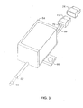
- FIGURE 3 provides a pictorial view of one embodiment of an interface module taught by this disclosure.
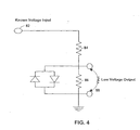
- FIGURE 4 describes how the ratio of resistances within the circuit may be determined with a known voltage point and measured voltage output.
- FIGUREs Preferred embodiments of the present invention are illustrated in the FIGUREs, like numerals being used to refer to like and corresponding parts of the various drawings.
- the disclosure provides a high voltage interface module used to reduce unsafe voltage to safe levels.
- a high or unsafe voltage input 32 is applied to circuit 30.
- Input voltage 32 drops across the voltage divider circuit having resistor 34 and resistor 36.
- the output voltage equals the portion of input voltage dropped across the terminals of resistor 36.
- the valve equals input voltage 32 reduced by the ratio of resistor 36 to the value of resistor 36 summed with resistor 34.
- Transorb 38 prevents a failure in either resistor 34 or resistor 36 from resulting in the presence of a shock or other electrical hazard. This hazard would be carried within leads 40 and 42, used to carry the output voltage to test equipments 44.
- Transorb 38 may comprise a pair of oppositely aligned diodes 46 and 48. When diode 46 breaks down, for example, at 40 volts. Such a condition may occur if resistor 34 were to short-circuit. Similarly, if resistor 36 were to open circuit, the resulting the output voltage across the terminals of resistor 36 would be shunted to the reference point or ground by diode 48. In this condition, terminals 50 and 52 are connected to the reference points where diode 48 shunts input voltage 32.
- This circuit designed to be installed at or near a high-voltage sampling point, reduces the need to run dangerous high-voltage leads from the sampling point to testing equipment 44.
- input voltage 32 is reduced by a ratio of 1/101.01.
- the output voltage may be limited by a 40-volt transorb in the event of any signal element failure.
- the reduced-voltage output measured across the terminals of resistor 36, runs to a data acquisition system or to a meter (display).
- this system employs passive components and requires no adjustments or calibration. Additionally, the described results eliminate the need for high-voltage leads in favor of low-voltage leads 40 and 42.
- the low-voltage leads carry voltages that do not pose a shock hazard to personnel or an electrical hazard to equipment. This reduces risk associated with testing complex equipment containing high or unsafe voltages and has many industrial applications.
- FIGURE 3 provides an isometric view of one embodiment of a high-voltage interface module.
- leads 60 and 62 couple to sampling points for a high-voltage output.
- this circuit is encapsulated within potted box enclosure 64. This enclosure protects technicians working on the circuit.
- Copper tab 66 serves as the reference or ground of the previously described circuit of FIGURE 2.
- Low-voltage leads 68 and 70 route the output voltage to data collection equipment. The connection passes through electrical connections 72 and 74.
- FIGURE 4 illustrates that a known voltage input 82 is applied to the circuit 85.
- Resistor 86 allows a low-voltage output measurement to be taken across terminals 88 of resistor 86.
- Equation 3 uses the empirically determined ratio of Equation 2 to determine the value of V unknown .
- V unknown V measured V in V out
- the ratio in Equation 2 may be recorded in data associated with the individual interface module for later use when sampling input voltages of an unknown value(s).
- the measured voltage is in Equation 3 shows that an unknown high-voltage input may be easily calculated as the product of a measured low voltage output (V measured ) and the inverse ratio described in Equation 2.
- the ratio of a known high-voltage input (V in ) to its measured low-voltage output (V out ) equals the ratio of the resistor values.
- the disclosed voltage interface module provides the ability to safely sample high-voltage signals and condition those signals locally at the point of measurement. Then these signals are routed via low-voltage leads to data collection equipment. This arrangement avoids potential shock hazards to which previous high-voltage measurement systems were susceptible.
- the present invention provides a safe and simple means to measure unsafe voltages in a complex system while protecting equipment and personnel from inadvertent and unexpected encounters with high-voltages. This system has numerous industrial applications, and ensures that should a signal element failure occur, the output of the interface module remains at a safe voltage level.
Landscapes
- Physics & Mathematics (AREA)
- General Physics & Mathematics (AREA)
- Emergency Protection Circuit Devices (AREA)
Applications Claiming Priority (2)
| Application Number | Priority Date | Filing Date | Title |
|---|---|---|---|
| US10/659,890 US6937026B2 (en) | 2003-09-11 | 2003-09-11 | High voltage interface module |
| US659890 | 2003-09-11 |
Publications (1)
| Publication Number | Publication Date |
|---|---|
| EP1515145A1 true EP1515145A1 (de) | 2005-03-16 |
Family
ID=34136766
Family Applications (1)
| Application Number | Title | Priority Date | Filing Date |
|---|---|---|---|
| EP04021302A Withdrawn EP1515145A1 (de) | 2003-09-11 | 2004-09-08 | Hochspannung-schnittstellenmodul |
Country Status (2)
| Country | Link |
|---|---|
| US (1) | US6937026B2 (de) |
| EP (1) | EP1515145A1 (de) |
Cited By (5)
| Publication number | Priority date | Publication date | Assignee | Title |
|---|---|---|---|---|
| EP1863158A3 (de) * | 2006-05-29 | 2008-12-24 | Samsung Electronics Co., Ltd. | Stromversorgungsvorrichtung |
| GB2482534A (en) * | 2010-08-05 | 2012-02-08 | Siemens Plc | Superconducting coil node voltage divider with externally selectable resistor |
| CN103048585A (zh) * | 2013-01-29 | 2013-04-17 | 重庆市智能水表有限责任公司 | 一种红外光电对管开路故障在线检测方法 |
| CN104006857A (zh) * | 2014-06-10 | 2014-08-27 | 深圳市骏普科技开发有限公司 | 一种光电直读水表传感器抑制气泡干扰的方法 |
| EP3825701A1 (de) * | 2019-11-19 | 2021-05-26 | General Electric Company | Leistungselektronikanordnung mit einer vergossenen hochspannungsdämpfungskarte für eine windturbine |
Families Citing this family (3)
| Publication number | Priority date | Publication date | Assignee | Title |
|---|---|---|---|---|
| DE102015215801A1 (de) * | 2015-08-19 | 2017-02-23 | Siemens Aktiengesellschaft | Eigenversorgte Messvorrichtung und Messverfahren |
| US12313684B2 (en) | 2019-07-01 | 2025-05-27 | Gillig Llc | High-voltage system test measurement systems and methods |
| US12444556B2 (en) | 2019-07-03 | 2025-10-14 | Gillig Llc | High-voltage system test measurement systems and methods |
Citations (5)
| Publication number | Priority date | Publication date | Assignee | Title |
|---|---|---|---|---|
| JPS5733364A (en) * | 1980-08-06 | 1982-02-23 | Hitachi Ltd | Voltage divider for high voltage |
| DE3714945A1 (de) * | 1986-05-09 | 1987-11-12 | Koch & Sterzel Kg | Frequenzunabhaengiger kapazitiv-ohmscher spannungsteiler zum messen von hochspannungen in mittel- und hochfrequenten roentgengeneratoren |
| GB2217856A (en) * | 1988-04-18 | 1989-11-01 | Queensland Electricity Commiss | Testing high voltage devices |
| US5107202A (en) * | 1989-10-23 | 1992-04-21 | Trustees Of Princeton University | Fiber optic current monitor for high-voltage applications |
| WO1999015906A1 (de) * | 1997-09-23 | 1999-04-01 | Trench Switzerland Ag | Kombinierter kleinsignal-strom- und spannungswandler |
Family Cites Families (5)
| Publication number | Priority date | Publication date | Assignee | Title |
|---|---|---|---|---|
| US4099216A (en) * | 1976-11-12 | 1978-07-04 | Westinghouse Electric Corp. | Fuseless intrinsic safety barrier |
| JPS55107132A (en) | 1979-02-09 | 1980-08-16 | Akebono Brake Ind Co Ltd | Working oil circulation circuit for wet type disc brake |
| US4698740A (en) * | 1986-02-14 | 1987-10-06 | Westinghouse Electric Corp. | Current fed regulated voltage supply |
| US4835462A (en) * | 1988-02-01 | 1989-05-30 | The United States Of America As Represented By The Secretary Of The Navy | Means for proximal end measurement of AC voltage across distal end cable load |
| US5644215A (en) * | 1995-06-07 | 1997-07-01 | Micron Technology, Inc. | Circuit and method for regulating a voltage |
-
2003
- 2003-09-11 US US10/659,890 patent/US6937026B2/en not_active Expired - Fee Related
-
2004
- 2004-09-08 EP EP04021302A patent/EP1515145A1/de not_active Withdrawn
Patent Citations (5)
| Publication number | Priority date | Publication date | Assignee | Title |
|---|---|---|---|---|
| JPS5733364A (en) * | 1980-08-06 | 1982-02-23 | Hitachi Ltd | Voltage divider for high voltage |
| DE3714945A1 (de) * | 1986-05-09 | 1987-11-12 | Koch & Sterzel Kg | Frequenzunabhaengiger kapazitiv-ohmscher spannungsteiler zum messen von hochspannungen in mittel- und hochfrequenten roentgengeneratoren |
| GB2217856A (en) * | 1988-04-18 | 1989-11-01 | Queensland Electricity Commiss | Testing high voltage devices |
| US5107202A (en) * | 1989-10-23 | 1992-04-21 | Trustees Of Princeton University | Fiber optic current monitor for high-voltage applications |
| WO1999015906A1 (de) * | 1997-09-23 | 1999-04-01 | Trench Switzerland Ag | Kombinierter kleinsignal-strom- und spannungswandler |
Non-Patent Citations (1)
| Title |
|---|
| PATENT ABSTRACTS OF JAPAN vol. 0061, no. 00 (P - 121) 9 June 1982 (1982-06-09) * |
Cited By (10)
| Publication number | Priority date | Publication date | Assignee | Title |
|---|---|---|---|---|
| EP1863158A3 (de) * | 2006-05-29 | 2008-12-24 | Samsung Electronics Co., Ltd. | Stromversorgungsvorrichtung |
| GB2482534A (en) * | 2010-08-05 | 2012-02-08 | Siemens Plc | Superconducting coil node voltage divider with externally selectable resistor |
| CN102376412A (zh) * | 2010-08-05 | 2012-03-14 | 英国西门子公司 | 用于超导磁体的线圈节点电压输出端 |
| GB2482534B (en) * | 2010-08-05 | 2012-08-15 | Siemens Plc | Coil node voltage outputs for superconducting magnets |
| CN102376412B (zh) * | 2010-08-05 | 2016-04-20 | 英国西门子公司 | 用于超导磁体的线圈节点电压输出端 |
| CN103048585A (zh) * | 2013-01-29 | 2013-04-17 | 重庆市智能水表有限责任公司 | 一种红外光电对管开路故障在线检测方法 |
| CN104006857A (zh) * | 2014-06-10 | 2014-08-27 | 深圳市骏普科技开发有限公司 | 一种光电直读水表传感器抑制气泡干扰的方法 |
| CN104006857B (zh) * | 2014-06-10 | 2017-10-20 | 深圳市骏普科技开发有限公司 | 一种光电直读水表传感器抑制气泡干扰的方法 |
| EP3825701A1 (de) * | 2019-11-19 | 2021-05-26 | General Electric Company | Leistungselektronikanordnung mit einer vergossenen hochspannungsdämpfungskarte für eine windturbine |
| US11664715B2 (en) | 2019-11-19 | 2023-05-30 | General Electric Company | Power electronics assembly having a potted high voltage attenuator card for a wind turbine |
Also Published As
| Publication number | Publication date |
|---|---|
| US6937026B2 (en) | 2005-08-30 |
| US20050057260A1 (en) | 2005-03-17 |
Similar Documents
| Publication | Publication Date | Title |
|---|---|---|
| US4389695A (en) | Equipment for protecting electronic equipment and personnel against inadvertent occurrence of extended or transient high voltages and method | |
| US5412526A (en) | Surge arrester circuit and housing therefor | |
| US4099216A (en) | Fuseless intrinsic safety barrier | |
| US8179653B2 (en) | Multiple operating voltage electrical surge protection apparatus | |
| US6477025B1 (en) | Surge protection device with thermal protection, current limiting, and failure indication | |
| US3527985A (en) | Electrical barrier device | |
| US6937026B2 (en) | High voltage interface module | |
| US20070121269A1 (en) | Earthing and overvoltage protection arrangement | |
| CA2289270A1 (en) | Data surge protection module | |
| EP1403832B2 (de) | Intrinsisch sichere explosionssichere sensorschaltung | |
| GB2131558A (en) | Measuring potential difference | |
| WO2014026933A1 (de) | Sicherungsausfallanzeige | |
| US12259412B2 (en) | Surge protection device integrating a current measurement sensor | |
| US7215519B2 (en) | Ground and line fault interrupt controller/adapter | |
| WO1993004517A1 (en) | Improved lightning protection for field mounted instruments | |
| US5751536A (en) | Method and apparatus for providing isolation from hazardous voltage levels in a hybrid instrumentation system | |
| US20240283193A1 (en) | Hazardous environment electrical feedback barrier device, assembly, system and method | |
| US4301403A (en) | Electrical circuit testing | |
| US12288948B1 (en) | Power cable plug connector | |
| US8143895B2 (en) | Coil node voltage outputs for superconducting magnets | |
| US6163445A (en) | Low-voltage test signal path protection circuit with extended bandwidth, overvoltage and transient protection | |
| US12253546B2 (en) | Voltage presence determination system for a high voltage electrical network | |
| US6239961B1 (en) | Overvoltage protection circuit | |
| US11942244B2 (en) | Surge protection apparatus and method for substation protective relays | |
| DE582742C (de) | Einrichtung zur UEberwachung des Isolationszustandes von Wechselstromgeneratoren, Transformatoren u. dgl. |
Legal Events
| Date | Code | Title | Description |
|---|---|---|---|
| PUAI | Public reference made under article 153(3) epc to a published international application that has entered the european phase |
Free format text: ORIGINAL CODE: 0009012 |
|
| AK | Designated contracting states |
Kind code of ref document: A1 Designated state(s): AT BE BG CH CY CZ DE DK EE ES FI FR GB GR HU IE IT LI LU MC NL PL PT RO SE SI SK TR |
|
| AX | Request for extension of the european patent |
Extension state: AL HR LT LV MK |
|
| 17P | Request for examination filed |
Effective date: 20050916 |
|
| AKX | Designation fees paid |
Designated state(s): DE FR GB IT |
|
| GRAP | Despatch of communication of intention to grant a patent |
Free format text: ORIGINAL CODE: EPIDOSNIGR1 |
|
| RTI1 | Title (correction) |
Free format text: HIGH VOLTAGE INTERFACE MODULE AND ASSOCIATED METHOD |
|
| STAA | Information on the status of an ep patent application or granted ep patent |
Free format text: STATUS: THE APPLICATION IS DEEMED TO BE WITHDRAWN |
|
| 18D | Application deemed to be withdrawn |
Effective date: 20100817 |