EP1513203A2 - Lichtemittierende Halbleitervorrichtung und Herstellungsverfahren - Google Patents
Lichtemittierende Halbleitervorrichtung und Herstellungsverfahren Download PDFInfo
- Publication number
- EP1513203A2 EP1513203A2 EP04255416A EP04255416A EP1513203A2 EP 1513203 A2 EP1513203 A2 EP 1513203A2 EP 04255416 A EP04255416 A EP 04255416A EP 04255416 A EP04255416 A EP 04255416A EP 1513203 A2 EP1513203 A2 EP 1513203A2
- Authority
- EP
- European Patent Office
- Prior art keywords
- layer
- light emitting
- ohmic contact
- type clad
- emitting device
- Prior art date
- Legal status (The legal status is an assumption and is not a legal conclusion. Google has not performed a legal analysis and makes no representation as to the accuracy of the status listed.)
- Withdrawn
Links
Images



Classifications
-
- H—ELECTRICITY
- H10—SEMICONDUCTOR DEVICES; ELECTRIC SOLID-STATE DEVICES NOT OTHERWISE PROVIDED FOR
- H10H—INORGANIC LIGHT-EMITTING SEMICONDUCTOR DEVICES HAVING POTENTIAL BARRIERS
- H10H20/00—Individual inorganic light-emitting semiconductor devices having potential barriers, e.g. light-emitting diodes [LED]
- H10H20/80—Constructional details
- H10H20/83—Electrodes
- H10H20/832—Electrodes characterised by their material
- H10H20/835—Reflective materials
-
- H—ELECTRICITY
- H10—SEMICONDUCTOR DEVICES; ELECTRIC SOLID-STATE DEVICES NOT OTHERWISE PROVIDED FOR
- H10H—INORGANIC LIGHT-EMITTING SEMICONDUCTOR DEVICES HAVING POTENTIAL BARRIERS
- H10H20/00—Individual inorganic light-emitting semiconductor devices having potential barriers, e.g. light-emitting diodes [LED]
- H10H20/01—Manufacture or treatment
- H10H20/032—Manufacture or treatment of electrodes
-
- H—ELECTRICITY
- H10—SEMICONDUCTOR DEVICES; ELECTRIC SOLID-STATE DEVICES NOT OTHERWISE PROVIDED FOR
- H10H—INORGANIC LIGHT-EMITTING SEMICONDUCTOR DEVICES HAVING POTENTIAL BARRIERS
- H10H20/00—Individual inorganic light-emitting semiconductor devices having potential barriers, e.g. light-emitting diodes [LED]
- H10H20/80—Constructional details
- H10H20/81—Bodies
- H10H20/822—Materials of the light-emitting regions
- H10H20/824—Materials of the light-emitting regions comprising only Group III-V materials, e.g. GaP
- H10H20/825—Materials of the light-emitting regions comprising only Group III-V materials, e.g. GaP containing nitrogen, e.g. GaN
-
- H—ELECTRICITY
- H10—SEMICONDUCTOR DEVICES; ELECTRIC SOLID-STATE DEVICES NOT OTHERWISE PROVIDED FOR
- H10H—INORGANIC LIGHT-EMITTING SEMICONDUCTOR DEVICES HAVING POTENTIAL BARRIERS
- H10H20/00—Individual inorganic light-emitting semiconductor devices having potential barriers, e.g. light-emitting diodes [LED]
- H10H20/80—Constructional details
- H10H20/83—Electrodes
- H10H20/832—Electrodes characterised by their material
- H10H20/833—Transparent materials
Definitions
- the present invention relates to a light emitting device and a method of manufacturing the same, and more particularly, to a light emitting device having a reflective electrode structure wherein ohmic characteristics are improved and a method of manufacturing the light emitting device.
- GaN gallium nitride
- Such GaN light emitting devices are classified into top-emitting light emitting diodes (TLEDS) and flip-chip light emitting diodes (FCLEDS).
- TLEDS emit light through an ohmic contact layer in direct contact with a p-type clad layer while the low electric conductivity of the p-type clad layer provides current injection through a transparent ohmic contact layer having a low ohmic value without obstructions.
- TLEDS generally have a structure wherein a nickel (Ni) layer and a gold (Au) layer are successively stacked over a p-type clad layer.
- Ni layer forms a semi-transparent ohmic contact layer having a specific contact resistance of 10 -3 to 10 -4 ⁇ cm 2 through annealing in O 2 ambient.
- the low specific contact resistance of the semi-transparent ohmic contact layer is formed between a Ni layer and a GaN forming a p-type clad layer and between the Ni layer and an Au layer when an annealing at a temperature of 500-600°C is performed in O 2 ambient, thus resulting in lowering Schottky barrier height (SBH) and easily providing holes, being multiple carriers, onto around the surface of the p-type clad layer. Therefore, the effective carrier concentration in the vicinity of the p-type clad layer surface increases.
- SBH Schottky barrier height
- a Ni layer and a Au layer formed over a p-type clad layer show characteristics of ohmic conduction through annealing, wherein the reactivation process removing compounds among Mg-H metals and increasing the concentration of Mg dopant on the surface of GaN makes the effective carrier concentration more than 10 19 on the surface of the p-type clad layer and causes a tunneling conduction between the p-type clad layer and the ohmic contact layer containing NiO.
- TLEDS employing a semi-transparent electrode thin film made of Ni and Au have low light efficiency, thus making it difficult to realize a light emitting device having a large capacity and high brightness.
- metals have high reflective efficiency and thus provide high light emitting efficiency.
- the metals have small work function, resulting in making the life span of a light emitting device short because of the difficulty to form an ohmic contact having a low ohmic value and failing to provide a stable light emitting device because of the poor adhesive property to GaN.
- a light emitting device having a light emitting layer between an n-type clad layer and a p-type clad layer comprises: a reflective layer reflecting light emitted from the light emitting layer and an ohmic contact layer formed by adding an additional element to an indium oxide between the reflective layer and the p-type clad layer.
- the present invention provides a light emitting device having an electrode structure wherein a low ohmic value and high reflective efficiency are achieved and a method of manufacturing the light emitting device.
- Examples of the additional element may include at least one element selected from the group consisting of Mg, Ag, Zn, Sc, Hf, Zr, Te, Se, Ta, W, Nb, Cu, Si, Ni, Co, Mo, Cr, Mn, Hg, Pr, and lanthanide (Ln).
- the addition rate of the additional element to an indium oxide may be 0.1-49 atomic percent.
- the reflective layer may be made of at least one selected from the group consisting of rhodium (Rh), Ag, and zinc (Zn).
- the thickness of the ohmic contact layer may be 0.1-100nm.
- a substrate may be formed in the lower part of the n-type clad layer and be made of a material transmitting light.
- a method of manufacturing a light emitting device having a light emitting layer between an n-type clad layer and a p-type clad layer comprising: forming an ohmic contact layer by adding an additional element to an indium oxide on the p-type clad layer of a light emitting a structure wherein a n-type clad layer, light emitting layer, and a p-type clad layer are successively stacked on a substrate; and forming a reflective layer over the ohmic contact layer; annealing a resultant structure in which the reflective layer is formed.
- Examples of the additional element in the process of forming the ohmic contact layer may include at least one element selected from the group consisting of Mg, Ag, Zn, Sc, Hf, Zr, Te, Se, Ta, W, Nb, Cu, Si, Ni, Co, Mo, Cr, Mn, Hg, Pr, and lanthanide (Ln).
- the annealing may be done at a temperature between 200°C and 700°C
- the annealing may be performed in gas ambient including at least one element selected from the group consisting of nitrogen, argon, helium, oxygen, hydrogen, and air in a reactor equipped with the stacked structure.
- the annealing may be performed in vacuum condition of the interior of a reactor equipped with the resultant structure.
- the annealing may be done for a period ranging between 10 seconds and 2 hours.
- the ohmic contact layer may be formed with a device selected from the group consisting of an electron-beam evaporator, thermal evaporator, and dual-type thermal evaporator.
- a p-type electrode structure includes an ohmic contact layer 30 and a reflective layer 40.
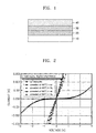
- FIG.1 illustrates a structure wherein the ohmic contact layer 30 and the reflective layer 40 are successively stacked on a group III nitride based p-type clad layer 20 formed on a substrate 10 in order to experiment on the characteristics between a p-type electrode structure and a p-type clad layer requiring improved ohmic characteristics.
- the p-type clad layer is formed in opposition to the n-type clad layer each other centering around a light emitting layer of a group III nitride based light emitting device.
- a group III nitride compound added with a p-type dopant can be used as the p-type clad layer 20.
- the group III nitride compound for example, can be expressed as Al x In y Ga z N wherein 0 ⁇ x ⁇ 1,0 ⁇ y ⁇ 1,0 ⁇ z ⁇ 1, and 0 ⁇ x+y+z ⁇ 1.
- Examples of the p-type dopant include Mg, Zn, Ca, Sr, Ba, and the like.
- the ohmic contact layer 30 is formed by adding a predetermined additional element for improving characteristics to an indium oxide, for example, In 2 O 3 .
- the additional element is preferably a material that can form the ohmic contact layer 30 having improved ohmic characteristics by controlling band gap, electron affinity, and work function of the indium oxide.
- Metal increasing effective carrier concentration and having good preferential reactivity with components other than nitrogen among compounds composing the p-type clad layer 20 are employed as materials suitable for the additional element in the ohmic contact layer 30.
- the additional element that preferentially reacts with gallium (Ga) prior to nitrogen is added to the indium oxide in the ohmic contact layer 30.
- Ga vacancy is formed over the surface of the p-type clad layer 30 through the reaction between Ga of the p-type clad layer 20 and the ohmic contact layer 30 because of the ohmic contact layer 30 having the above described characteristics.
- the Ga vacancy formed over the p-type clad layer 20 acts as a p-type dopant, thus increasing effective p-type carrier concentration on the surface of the p-type clad layer 20 by the reaction between the p-type clad layer 20 and the ohmic contact layer 30.
- materials that remain behind over the surface of the p-type clad layer in the forming process and are able to form transparent conductive oxide by reacting with gallium oxide (Ga 2 O 3 ), which is a natural oxide layer obstructing the flow of carriers in the interface between the p-type clad layer 20 and the ohmic contact layer 30, are employed in the ohmic contact layer 30.
- gallium oxide Ga 2 O 3
- the additional element added to In 2 O 3 of the ohmic contact layer 30 can be at least one selected from the group consisting of Mg, Ag, Zn, Sc, Hf, Zr, Te, Se, Ta, W, Nb, Cu, Si, Ni, Co, Mo, Cr, Mn, Hg, Pr, and lanthanide (Ln).
- the addition rate of the additional element to the indium oxide is preferably in the range of 0.1-49 atomic percent.
- the atomic percent refers to the rate between the numbers of the added element.
- the thickness of the ohmic contact layer 30 is preferably in the range of 0.1-100 nm.
- the reflective layer 40 is the uppermost layer of the p-type electrode structure.
- the reflective layer 40 may be formed using a material that has the restrained surface degradation in the range of 300-600°C, the temperature range generally applied in the process of manufacturing FCLEDS, is stable to oxidation, and has high reflective capability without changing the characteristics.
- the reflective layer 40 can be formed of one selected from the group consisting of Rh, Ag, and Zn.
- the thickness of the reflective layer 40 may be 10-1000nm.
- the ohmic contact layer 30 and the reflective layer 40 may be formed by an electron-beam evaporator.
- the ohmic contact layer 30 and the reflective layer 40 may be formed by various known evaporating methods except for the sputtering method, for example, physical vapor deposition (PVD), chemical vapor deposition (CVD), plasma laser deposition (PLD), thermal evaporator, dual-type thermal evaporator, and the like.
- PVD physical vapor deposition
- CVD chemical vapor deposition
- PLAD plasma laser deposition
- thermal evaporator dual-type thermal evaporator, and the like.
- the evaporation is performed at the range of 20-1500°C and the pressure at the interior of the reactor is an atmosphere to about 10- 12 torr.
- the sputtering is difficult to apply because the GaN based p-type clad layer 30 is changed into an insulator due to the damage from plasma in the process of forming the p-type electrode structure.
- the ohmic contact layer 30 and the reflective layer 40 undergo annealing process after the evaporation process.
- Annealing is done at the temperature of 200-700°C in vacuum or gas ambient for about 10 seconds to 2 hours.
- At least one element selected from the group consisting of nitrogen, argon, helium, oxygen, hydrogen, and air may be injected into the interior of a reactor.
- a structure wherein the p-type clad layer 20 made up mainly of GaN is formed over the substrate, is washed in an ultrasonic bath at the temperature of 60°C for 5 minutes respectively by trichloroethylene, acetone, methanol, and distilled water and undergoes hard baking at the temperature of 100°C for 10 minutes in order to eliminate remaining water from the sample.
- photo-resist undergoes spin coating over the p-type clad layer 20 at 4.500rpm.
- the photo-resist undergoes soft baking at the temperature of 85°C for 15 minutes.
- a mask and the sample are aligned in order to develop a mask pattern and are exposed in ultraviolet rays (UV) of 22.8mW for 15 seconds.
- UV ultraviolet rays
- the sample is soaked in the solution, wherein developing solution and distilled water are mixed at the rate of 1 to 4, for 25 seconds and is developed.
- the sample is soaked in BOE solution for 5 minutes. Then, the ohmic contact layer 30 is evaporated by an electron-beam evaporator.
- the ohmic contact layer 30 is evaporated by mounting a reaction object, formed by mixing In 2 O 3 powder with oxide magnesium (MgO) at the rate of 9 to 1 and sintering the mixture, at a reaction object mounting stage in the chamber of an electron-beam evaporator.
- a reaction object formed by mixing In 2 O 3 powder with oxide magnesium (MgO) at the rate of 9 to 1 and sintering the mixture, at a reaction object mounting stage in the chamber of an electron-beam evaporator.
- the reflective layer 40 is evaporated by Ag and undergoes lift-off process with acetone. Then, an electrode structure is manufactured by annealing the sample in a rapid thermal annealing (RTA) furnace at the temperature of 330-530°C for 1 minute.
- RTA rapid thermal annealing
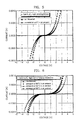
- FIGS. 2 through 4 are a graph showing the result of measuring the electric characteristics of the ohmic contact layer 30 and the reflective layer 40 which were sequentially formed in different thickness on the p-type clad layer 20 having GaN of carrier concentration of 4 ⁇ 5 ⁇ 10 17 cm -3 as a main component wherein the ohmic contact layer 30 was formed so that Mg is contained in the indium oxide and the reflective layer 40 was formed of Ag. Also, the ohmic contact layer 30 and the reflective layer 40 were annealed at the temperature of 330-530°C in air ambient before the measure.
- FIG. 2 is a graph showing the result of measuring the electric characteristics when the thicknesses of the ohmic contact layer 30 and the reflective layer 40 were 5nm and 100nm, respectively.
- FIG. 3 is a graph showing the result of measuring the electric characteristics when the thickness of the ohmic contact layer 30 was 2.5nm and that of the reflective layer 40 was 200nm.
- FIG.4 is when the thickness of the ohmic contact layer 30 was 5nm and that of the reflective layer 40 was 200nm.
- FIGS 5 and 6 show the result of comparing the characteristics in such a case that an additional element was added to the indium oxide with the characteristics in a conventional case that no the additional element was added.
- FIG. 5 shows the result of measuring the characteristics of electric current and voltage of the sample before and after annealing at the temperature of 530°C in air ambient when an In 2 O 3 layer was evaporated at the thickness of 2.5nm over a p-type clad layer with In 2 O 3 alone without adding any other element and a reflective layer was evaporated at the thickness of 200nm on the In 2 O 3 layer with aluminum.
- the characteristics of electric current and voltage were non-linear in the In 2 O 3 layer without having any added element regardless of annealing.
- FIG. 6 shows the result of measuring the characteristics of electric current and voltage of the sample before and after annealing at the temperature of 330-530°C in air ambient when an ohmic contact layer with Mg added to In 2 O 3 was deposited to the thickness of 2.5nm on a p-type clad layer and a titanium layer was deposited to the thickness of 10 nm and a reflective layer was deposited to the thickness of 200nm on the ohmic contact layer with aluminum.
- Material forming the ohmic contact layer 30 is oxide having high light transmittance and high conductivity.
- the ohmic contact layer 30 is formed by adding an additional element to In 2 O 3 through doping or mixing in order to control band gap, electron affinity, and work function, which determine the electrical characteristics of the ohmic contact layer 30 in contact with the p-type clad layer 20.
- the ohmic contact layer 30 made of the oxide forms a transparent conductive oxide, GaInO3, in reaction with Ga 2 O 3 that is an oxide layer existing over the upper part of the p-type clad layer 20 in the process of annealing.
- the ohmic contact layer 30 forms Ga vacancy over the surface, thus increasing the effective hole concentration around the surface of the p-type clad layer 20.
- the formed oxide has considerably high work function value, resulting in lowering the height and width of SBH when it contacts with the p-type clad layer 20, thus improving the ohmic contact characteristics and providing light transmittance close to 100%.
- FIG. 7 is a view showing an example of a light emitting device employing the p-type electrode structure of FIG. 1.
- the light emitting device has a structure wherein a substrate 110, a buffer layer 120, an n-type clad layer 130, a light emitting layer 140, a p-type clad layer 150, an ohmic contact layer 230, and a reflective layer 240 are successively stacked.
- Reference numeral 180 denotes a p-type electrode pad and reference numeral 190 an n-type electrode pad.
- the substrate 110 is made of a transparent material such as sapphire or silicon carbide (SiC).
- the buffer layer 120 can be omitted.
- Each layer from the buffer layer 120 to the p-type clad layer 150 is formed of mainly any one compound selected from the compounds expressed as a group III nitride based compounds, for example, Al x In y Ga z N(0 ⁇ x ⁇ 1,0 ⁇ y ⁇ 1,0 ⁇ z ⁇ 1, and 0 ⁇ x+y+z ⁇ 1).
- the appropriate dopant is added to the n-type clad layer 130 and the p-type clad layer 150.
- the light emitting layer 140 can be formed in various methods such as a single layer or a MQW layer.
- the buffet layer 120 is formed of GaN.
- the n-type clad layer 150 is formed by adding Si, Ge, Se, Te, and the like as an n-type dopant to GaN.
- the p-type clad layer 150 is formed by adding Mg, Zn, Ca,Sr, Ba, and the like as a p-type dopant to GaN.
- Each layer is formed by the above described evaporation method, for example, PVD, CVD, PLD, thermal evaporator, dual-type thermal evaporator, and the like.
- the ohmic contact layer 230 is formed by adding an additional element to In 2 O 3 as shown in FIG. 1 and the reflective layer 240 is formed of one selected from the group consisting of Ag, Rh, and Zn. Then the layers undergo annealing.
- the treatment of the surface of the p-type clad layer 150, which was exposed from a light emitting structure stacked with a substrate mainly formed of InGaN, a buffer layer, an n-type clad layer, a light emitting layer, and a p-type clad layer, and electron beam lithography process were same those of the example described with reference to FIG. 1 before evaporating a p-type electrode structure.
- Light emitting diodes were manufactured by annealing at the temperature of 530°C for 1 minute in air ambient after successively evaporating the ohmic contact layer 230 with In 2 O 3 , which contained Mg as an additional element after the surface treatment and the electron beam lithography process, and the reflective layer 240 with Ag by an electron beam evaporator, undergoing lift-off process with acetone, and putting a sample in a RTA.
- FIGS. 8 and 9 show the result from measuring the characteristics of operating voltage when the ohmic contact layer 230 and the reflective layer 240 in accordance with the-invention were blue light emitting diodes having mainly InGaN.
- the annealing in this case was conducted at the temperature of 530°C in air ambient.
- FIG. 8 shows a case wherein the thickness of the ohmic contact layer 30 was 5nm and that of the reflective layer 40 was 100nm.
- FIG. 9 shows the result of measuring the characteristics of electric current and voltage in each case that the thickness of the ohmic contact layer 30 was 2.5nm and 5nm respectively while the thickness of the reflective layer 40 was 200nm.
- a light emitting device employing a p-type electrode structure of the invention has improved operating characteristics considering the fact that operating voltage at 20mA was 3.14-3.15V.
- FIG. 10 shows the results of measuring the relationship between operating voltage and output power after annealing the ohmic contact layer 230 having different thickness over the p-type clad layer 150 in air ambient.
- InGaN blue light emitting diodes have a packaged MQW structure.
- the output power changes depending on the thickness of the ohmic contact layer 230 and that of the reflective layer 240 with Ag.
- the characteristics of ohmic contact with a p-type clad layer is improved, thus increasing the efficiency and yield of wire bonding during packaging FCLEDS. Also, it is possible to increase the light emitting efficiency and life span of light emitting devices due to the low contactless resistance and the excellent electric current and voltage characteristic.
Landscapes
- Led Devices (AREA)
- Electrodes Of Semiconductors (AREA)
Applications Claiming Priority (2)
| Application Number | Priority Date | Filing Date | Title |
|---|---|---|---|
| KR1020030062830A KR100571816B1 (ko) | 2003-09-08 | 2003-09-08 | 질화물계 발광소자 및 그 제조방법 |
| KR2003062830 | 2003-09-08 |
Publications (2)
| Publication Number | Publication Date |
|---|---|
| EP1513203A2 true EP1513203A2 (de) | 2005-03-09 |
| EP1513203A3 EP1513203A3 (de) | 2006-11-29 |
Family
ID=34132246
Family Applications (1)
| Application Number | Title | Priority Date | Filing Date |
|---|---|---|---|
| EP04255416A Withdrawn EP1513203A3 (de) | 2003-09-08 | 2004-09-07 | Lichtemittierende Halbleitervorrichtung und Herstellungsverfahren |
Country Status (5)
| Country | Link |
|---|---|
| US (2) | US7205576B2 (de) |
| EP (1) | EP1513203A3 (de) |
| JP (1) | JP2005086210A (de) |
| KR (1) | KR100571816B1 (de) |
| CN (1) | CN100474639C (de) |
Families Citing this family (16)
| Publication number | Priority date | Publication date | Assignee | Title |
|---|---|---|---|---|
| US7067849B2 (en) | 2001-07-17 | 2006-06-27 | Lg Electronics Inc. | Diode having high brightness and method thereof |
| US6949395B2 (en) | 2001-10-22 | 2005-09-27 | Oriol, Inc. | Method of making diode having reflective layer |
| US7148520B2 (en) | 2001-10-26 | 2006-12-12 | Lg Electronics Inc. | Diode having vertical structure and method of manufacturing the same |
| KR100624416B1 (ko) * | 2003-12-23 | 2006-09-18 | 삼성전자주식회사 | 플립칩형 질화물계 발광소자 및 그 제조방법 |
| KR100862456B1 (ko) * | 2004-12-04 | 2008-10-08 | 삼성전기주식회사 | 투명 전극 및 이를 구비하는 화합물 반도체 발광소자 |
| KR100638813B1 (ko) * | 2005-04-15 | 2006-10-27 | 삼성전기주식회사 | 플립칩형 질화물 반도체 발광소자 |
| KR100609117B1 (ko) * | 2005-05-03 | 2006-08-08 | 삼성전기주식회사 | 질화물계 반도체 발광소자 및 그 제조방법 |
| KR100661711B1 (ko) * | 2005-08-30 | 2006-12-26 | 엘지이노텍 주식회사 | 반사 전극을 구비한 질화물 반도체 발광소자 및 그 제조방법 |
| WO2010113238A1 (ja) * | 2009-04-03 | 2010-10-07 | パナソニック株式会社 | 窒化物系半導体素子およびその製造方法 |
| US9142743B2 (en) * | 2011-08-02 | 2015-09-22 | Kabushiki Kaisha Toshiba | High temperature gold-free wafer bonding for light emitting diodes |
| TWI593138B (zh) * | 2013-12-23 | 2017-07-21 | Nat Chunghsing Univ | Led |
| US20160284957A1 (en) * | 2015-03-23 | 2016-09-29 | Toshiba Corporation | REFLECTIVE CONTACT FOR GaN-BASED LEDS |
| US10361364B2 (en) * | 2017-06-14 | 2019-07-23 | International Business Machines Corporation | Co-fabrication of magnetic device structures with electrical interconnects having reduced resistance through increased conductor grain size |
| US12507508B2 (en) * | 2017-08-30 | 2025-12-23 | Xiamen San'an Optoelectronics Co., Ltd. | Micro light-emitting diode and micro light-emitting diode array |
| CN107681034B (zh) * | 2017-08-30 | 2019-11-12 | 天津三安光电有限公司 | 微型发光二极管及其制作方法 |
| CN112071768B (zh) * | 2020-09-04 | 2022-09-20 | 晶能光电(江西)有限公司 | P面工艺监测结构及方法、晶圆结构 |
Family Cites Families (17)
| Publication number | Priority date | Publication date | Assignee | Title |
|---|---|---|---|---|
| DE3324647A1 (de) * | 1983-07-08 | 1985-01-17 | Schott Glaswerke, 6500 Mainz | Tauchverfahren zur herstellung transparenter, elektrisch leitfaehiger, dotierter indiumoxidschichten |
| US6936859B1 (en) * | 1998-05-13 | 2005-08-30 | Toyoda Gosei Co., Ltd. | Light-emitting semiconductor device using group III nitride compound |
| JP3736181B2 (ja) * | 1998-05-13 | 2006-01-18 | 豊田合成株式会社 | Iii族窒化物系化合物半導体発光素子 |
| TW437104B (en) * | 1999-05-25 | 2001-05-28 | Wang Tien Yang | Semiconductor light-emitting device and method for manufacturing the same |
| JP2001111109A (ja) * | 1999-10-07 | 2001-04-20 | Sharp Corp | 窒化ガリウム系化合物半導体発光素子 |
| JP4024994B2 (ja) * | 2000-06-30 | 2007-12-19 | 株式会社東芝 | 半導体発光素子 |
| KR20020026737A (ko) * | 2000-10-02 | 2002-04-12 | 염근영 | 투명 오믹접합을 갖는 광전소자 및 그 제조방법 |
| JP4925512B2 (ja) * | 2001-02-16 | 2012-04-25 | スタンレー電気株式会社 | 波長変換型半導体素子 |
| TW492202B (en) * | 2001-06-05 | 2002-06-21 | South Epitaxy Corp | Structure of III-V light emitting diode (LED) arranged in flip chip configuration having structure for preventing electrostatic discharge |
| JP3912044B2 (ja) * | 2001-06-06 | 2007-05-09 | 豊田合成株式会社 | Iii族窒化物系化合物半導体発光素子の製造方法 |
| JP2003168823A (ja) * | 2001-09-18 | 2003-06-13 | Toyoda Gosei Co Ltd | Iii族窒化物系化合物半導体発光素子 |
| JP4084620B2 (ja) * | 2001-09-27 | 2008-04-30 | 信越半導体株式会社 | 発光素子及び発光素子の製造方法 |
| US6869820B2 (en) * | 2002-01-30 | 2005-03-22 | United Epitaxy Co., Ltd. | High efficiency light emitting diode and method of making the same |
| TW577178B (en) * | 2002-03-04 | 2004-02-21 | United Epitaxy Co Ltd | High efficient reflective metal layer of light emitting diode |
| KR100491968B1 (ko) * | 2002-03-25 | 2005-05-27 | 학교법인 포항공과대학교 | 갈륨나이트라이드계 광소자의 p형 오믹 전극의 제조방법 |
| US6958494B2 (en) * | 2003-08-14 | 2005-10-25 | Dicon Fiberoptics, Inc. | Light emitting diodes with current spreading layer |
| KR100624411B1 (ko) * | 2003-08-25 | 2006-09-18 | 삼성전자주식회사 | 질화물계 발광소자 및 그 제조방법 |
-
2003
- 2003-09-08 KR KR1020030062830A patent/KR100571816B1/ko not_active Expired - Fee Related
-
2004
- 2004-09-01 US US10/930,915 patent/US7205576B2/en not_active Expired - Lifetime
- 2004-09-07 EP EP04255416A patent/EP1513203A3/de not_active Withdrawn
- 2004-09-08 CN CNB2004101038182A patent/CN100474639C/zh not_active Expired - Lifetime
- 2004-09-08 JP JP2004261354A patent/JP2005086210A/ja active Pending
-
2007
- 2007-03-07 US US11/714,843 patent/US7541207B2/en not_active Expired - Lifetime
Non-Patent Citations (1)
| Title |
|---|
| CHEN AND LIN: "The Microstructures and Mechanical Properties of the Sn-Zn-Ag-Al-Ga Solder Alloys - the Effect of Ag", JOURNAL OF ELECTRONIC MATERIALS, vol. 31, no. 8, August 2002 (2002-08-01), pages 861 - 867 * |
Also Published As
| Publication number | Publication date |
|---|---|
| JP2005086210A (ja) | 2005-03-31 |
| US20050051783A1 (en) | 2005-03-10 |
| US7205576B2 (en) | 2007-04-17 |
| US7541207B2 (en) | 2009-06-02 |
| KR20050025871A (ko) | 2005-03-14 |
| US20070254391A1 (en) | 2007-11-01 |
| KR100571816B1 (ko) | 2006-04-17 |
| CN1619853A (zh) | 2005-05-25 |
| CN100474639C (zh) | 2009-04-01 |
| EP1513203A3 (de) | 2006-11-29 |
Similar Documents
| Publication | Publication Date | Title |
|---|---|---|
| US7541207B2 (en) | Light emitting device and method of manufacturing the same | |
| US7180094B2 (en) | Nitride-based light emitting device and method of manufacturing the same | |
| EP1810351B1 (de) | Gan-halbleiter-verbundleuchtelement | |
| US7973325B2 (en) | Reflective electrode and compound semiconductor light emitting device including the same | |
| KR100624411B1 (ko) | 질화물계 발광소자 및 그 제조방법 | |
| JP2011199319A (ja) | 薄膜電極、及びその製造方法 | |
| JP2011151426A (ja) | 高性能の窒化ガリウム系発光素子のための薄膜電極およびその製造方法 | |
| US20050040755A1 (en) | Transparent thin film electrode for light emitting diode and laser diode | |
| KR100764458B1 (ko) | 전극층, 이를 구비하는 발광소자 및 전극층 제조방법 | |
| KR100580627B1 (ko) | 플립칩형 질화물계 발광소자 및 그 제조방법 | |
| KR100589645B1 (ko) | 산화아연계 발광소자 및 그 제조방법 | |
| KR100574106B1 (ko) | 질화물계 발광소자 및 그 제조방법 | |
| KR100574103B1 (ko) | 플립칩형 질화물계 발광소자 및 그 제조방법 |
Legal Events
| Date | Code | Title | Description |
|---|---|---|---|
| PUAI | Public reference made under article 153(3) epc to a published international application that has entered the european phase |
Free format text: ORIGINAL CODE: 0009012 |
|
| AK | Designated contracting states |
Kind code of ref document: A2 Designated state(s): AT BE BG CH CY CZ DE DK EE ES FI FR GB GR HU IE IT LI LU MC NL PL PT RO SE SI SK TR |
|
| AX | Request for extension of the european patent |
Extension state: AL HR LT LV MK |
|
| PUAL | Search report despatched |
Free format text: ORIGINAL CODE: 0009013 |
|
| AK | Designated contracting states |
Kind code of ref document: A3 Designated state(s): AT BE BG CH CY CZ DE DK EE ES FI FR GB GR HU IE IT LI LU MC NL PL PT RO SE SI SK TR |
|
| AX | Request for extension of the european patent |
Extension state: AL HR LT LV MK |
|
| 17P | Request for examination filed |
Effective date: 20070321 |
|
| AKX | Designation fees paid |
Designated state(s): DE FR GB |
|
| 17Q | First examination report despatched |
Effective date: 20070709 |
|
| RAP1 | Party data changed (applicant data changed or rights of an application transferred) |
Owner name: GWANGJU INSTITUTE OF SCIENCE AND TECHNOLOGY Owner name: SAMSUNG LED CO., LTD. |
|
| GRAP | Despatch of communication of intention to grant a patent |
Free format text: ORIGINAL CODE: EPIDOSNIGR1 |
|
| RIC1 | Information provided on ipc code assigned before grant |
Ipc: H01L 33/42 20100101ALN20121024BHEP Ipc: H01L 33/40 20100101AFI20121024BHEP Ipc: H01L 33/32 20100101ALN20121024BHEP |
|
| RAP1 | Party data changed (applicant data changed or rights of an application transferred) |
Owner name: GWANGJU INSTITUTE OF SCIENCE AND TECHNOLOGY Owner name: SAMSUNG ELECTRONICS CO., LTD. |
|
| STAA | Information on the status of an ep patent application or granted ep patent |
Free format text: STATUS: THE APPLICATION IS DEEMED TO BE WITHDRAWN |
|
| 18D | Application deemed to be withdrawn |
Effective date: 20130403 |