EP1513196A2 - Elektrolumineszierende Anzeigevorrichtungen mit aktiver Matrix und deren Herstellungsverfahren - Google Patents
Elektrolumineszierende Anzeigevorrichtungen mit aktiver Matrix und deren Herstellungsverfahren Download PDFInfo
- Publication number
- EP1513196A2 EP1513196A2 EP04019148A EP04019148A EP1513196A2 EP 1513196 A2 EP1513196 A2 EP 1513196A2 EP 04019148 A EP04019148 A EP 04019148A EP 04019148 A EP04019148 A EP 04019148A EP 1513196 A2 EP1513196 A2 EP 1513196A2
- Authority
- EP
- European Patent Office
- Prior art keywords
- wire
- layer
- electrode
- forming
- insulating layer
- Prior art date
- Legal status (The legal status is an assumption and is not a legal conclusion. Google has not performed a legal analysis and makes no representation as to the accuracy of the status listed.)
- Ceased
Links
- 238000000034 method Methods 0.000 title claims abstract description 34
- 238000005401 electroluminescence Methods 0.000 title claims abstract description 27
- 239000011159 matrix material Substances 0.000 title claims abstract description 24
- 239000000758 substrate Substances 0.000 claims abstract description 31
- 239000010410 layer Substances 0.000 claims description 145
- 229910052751 metal Inorganic materials 0.000 claims description 31
- 239000002184 metal Substances 0.000 claims description 31
- 239000011241 protective layer Substances 0.000 claims description 20
- PXHVJJICTQNCMI-UHFFFAOYSA-N Nickel Chemical compound [Ni] PXHVJJICTQNCMI-UHFFFAOYSA-N 0.000 claims description 15
- 239000010949 copper Substances 0.000 claims description 10
- 239000010931 gold Substances 0.000 claims description 10
- 239000010936 titanium Substances 0.000 claims description 10
- 229910052782 aluminium Inorganic materials 0.000 claims description 9
- XAGFODPZIPBFFR-UHFFFAOYSA-N aluminium Chemical compound [Al] XAGFODPZIPBFFR-UHFFFAOYSA-N 0.000 claims description 9
- AMGQUBHHOARCQH-UHFFFAOYSA-N indium;oxotin Chemical compound [In].[Sn]=O AMGQUBHHOARCQH-UHFFFAOYSA-N 0.000 claims description 8
- 239000000463 material Substances 0.000 claims description 8
- VYZAMTAEIAYCRO-UHFFFAOYSA-N Chromium Chemical compound [Cr] VYZAMTAEIAYCRO-UHFFFAOYSA-N 0.000 claims description 5
- RYGMFSIKBFXOCR-UHFFFAOYSA-N Copper Chemical compound [Cu] RYGMFSIKBFXOCR-UHFFFAOYSA-N 0.000 claims description 5
- 229910052779 Neodymium Inorganic materials 0.000 claims description 5
- BQCADISMDOOEFD-UHFFFAOYSA-N Silver Chemical compound [Ag] BQCADISMDOOEFD-UHFFFAOYSA-N 0.000 claims description 5
- RTAQQCXQSZGOHL-UHFFFAOYSA-N Titanium Chemical compound [Ti] RTAQQCXQSZGOHL-UHFFFAOYSA-N 0.000 claims description 5
- 229910052802 copper Inorganic materials 0.000 claims description 5
- PCHJSUWPFVWCPO-UHFFFAOYSA-N gold Chemical compound [Au] PCHJSUWPFVWCPO-UHFFFAOYSA-N 0.000 claims description 5
- 229910052737 gold Inorganic materials 0.000 claims description 5
- QEFYFXOXNSNQGX-UHFFFAOYSA-N neodymium atom Chemical compound [Nd] QEFYFXOXNSNQGX-UHFFFAOYSA-N 0.000 claims description 5
- 229910052759 nickel Inorganic materials 0.000 claims description 5
- 229910052709 silver Inorganic materials 0.000 claims description 5
- 239000004332 silver Substances 0.000 claims description 5
- 229910052715 tantalum Inorganic materials 0.000 claims description 5
- GUVRBAGPIYLISA-UHFFFAOYSA-N tantalum atom Chemical compound [Ta] GUVRBAGPIYLISA-UHFFFAOYSA-N 0.000 claims description 5
- 229910052719 titanium Inorganic materials 0.000 claims description 5
- WFKWXMTUELFFGS-UHFFFAOYSA-N tungsten Chemical compound [W] WFKWXMTUELFFGS-UHFFFAOYSA-N 0.000 claims description 5
- 229910052721 tungsten Inorganic materials 0.000 claims description 5
- 239000010937 tungsten Substances 0.000 claims description 5
- 229910000838 Al alloy Inorganic materials 0.000 claims description 4
- ZOKXTWBITQBERF-UHFFFAOYSA-N Molybdenum Chemical compound [Mo] ZOKXTWBITQBERF-UHFFFAOYSA-N 0.000 claims description 3
- 238000000151 deposition Methods 0.000 claims description 3
- 229910052750 molybdenum Inorganic materials 0.000 claims description 3
- 239000011733 molybdenum Substances 0.000 claims description 3
- 230000009972 noncorrosive effect Effects 0.000 claims description 2
- 230000000149 penetrating effect Effects 0.000 claims description 2
- 230000002708 enhancing effect Effects 0.000 abstract description 2
- 239000011229 interlayer Substances 0.000 description 7
- 239000007769 metal material Substances 0.000 description 5
- 230000008901 benefit Effects 0.000 description 4
- 239000012044 organic layer Substances 0.000 description 3
- 238000002161 passivation Methods 0.000 description 3
- 239000010409 thin film Substances 0.000 description 3
- 229910001182 Mo alloy Inorganic materials 0.000 description 2
- 229910004205 SiNX Inorganic materials 0.000 description 2
- VYPSYNLAJGMNEJ-UHFFFAOYSA-N Silicium dioxide Chemical group O=[Si]=O VYPSYNLAJGMNEJ-UHFFFAOYSA-N 0.000 description 2
- QVGXLLKOCUKJST-UHFFFAOYSA-N atomic oxygen Chemical compound [O] QVGXLLKOCUKJST-UHFFFAOYSA-N 0.000 description 2
- 239000011521 glass Substances 0.000 description 2
- 238000002347 injection Methods 0.000 description 2
- 239000007924 injection Substances 0.000 description 2
- 239000011810 insulating material Substances 0.000 description 2
- 238000012986 modification Methods 0.000 description 2
- 230000004048 modification Effects 0.000 description 2
- 229910052760 oxygen Inorganic materials 0.000 description 2
- 239000001301 oxygen Substances 0.000 description 2
- 230000001681 protective effect Effects 0.000 description 2
- 239000000565 sealant Substances 0.000 description 2
- 229910045601 alloy Inorganic materials 0.000 description 1
- 239000000956 alloy Substances 0.000 description 1
- 238000005260 corrosion Methods 0.000 description 1
- 230000007797 corrosion Effects 0.000 description 1
- 230000005281 excited state Effects 0.000 description 1
- 230000005283 ground state Effects 0.000 description 1
- 230000005525 hole transport Effects 0.000 description 1
- 238000002310 reflectometry Methods 0.000 description 1
- 239000000126 substance Substances 0.000 description 1
- 239000012780 transparent material Substances 0.000 description 1
Images


Classifications
-
- H—ELECTRICITY
- H10—SEMICONDUCTOR DEVICES; ELECTRIC SOLID-STATE DEVICES NOT OTHERWISE PROVIDED FOR
- H10K—ORGANIC ELECTRIC SOLID-STATE DEVICES
- H10K59/00—Integrated devices, or assemblies of multiple devices, comprising at least one organic light-emitting element covered by group H10K50/00
- H10K59/10—OLED displays
- H10K59/12—Active-matrix OLED [AMOLED] displays
- H10K59/131—Interconnections, e.g. wiring lines or terminals
-
- H—ELECTRICITY
- H05—ELECTRIC TECHNIQUES NOT OTHERWISE PROVIDED FOR
- H05B—ELECTRIC HEATING; ELECTRIC LIGHT SOURCES NOT OTHERWISE PROVIDED FOR; CIRCUIT ARRANGEMENTS FOR ELECTRIC LIGHT SOURCES, IN GENERAL
- H05B33/00—Electroluminescent light sources
- H05B33/10—Apparatus or processes specially adapted to the manufacture of electroluminescent light sources
-
- H—ELECTRICITY
- H10—SEMICONDUCTOR DEVICES; ELECTRIC SOLID-STATE DEVICES NOT OTHERWISE PROVIDED FOR
- H10K—ORGANIC ELECTRIC SOLID-STATE DEVICES
- H10K59/00—Integrated devices, or assemblies of multiple devices, comprising at least one organic light-emitting element covered by group H10K50/00
- H10K59/80—Constructional details
- H10K59/805—Electrodes
- H10K59/8052—Cathodes
-
- H—ELECTRICITY
- H10—SEMICONDUCTOR DEVICES; ELECTRIC SOLID-STATE DEVICES NOT OTHERWISE PROVIDED FOR
- H10K—ORGANIC ELECTRIC SOLID-STATE DEVICES
- H10K50/00—Organic light-emitting devices
- H10K50/80—Constructional details
- H10K50/805—Electrodes
- H10K50/82—Cathodes
Definitions
- the present invention relates to an organic electroluminescence device, and more particularly, to an active matrix electroluminescence device and a method for fabricating the same.
- the present invention is suitable for a wide scope of applications, it is particularly suitable for enhancing an electrical characteristic of wires outside of an emissive area of the device.
- An electroluminescence device is being viewed as a next generation flat display device for its characteristics of a wide viewing angle, a high aperture ratio, and a high chromaticity. More specifically, in an organic electroluminescence (EL) device, when an electric charge is injected into an organic luminous layer formed between a hole injection electrode and an electron injection electrode, the electron and the hole are paired to each other generating an exciton, the excited state of which falls to a ground state, thereby emitting light. Thus, the organic electroluminescence device (ELD) can be operated at a lower voltage, as compared to other display devices.
- EL organic electroluminescence
- the organic ELD can be classified into a passivation ELD and an active matrix ELD.
- the passivation ELD is formed of a transparent electrode on a transparent substrate, an organic electroluminous layer on the transparent electrode, and a cathode electrode on the organic electroluminous layer.
- the active matrix ELD is formed of a plurality of scan lines and data lines defining a pixel area on a substrate, a switching device electrically connecting the scan lines and the data lines and controlling the electroluminescence device, a transparent electrode (i.e. , anode) electrically connected to the switching device and formed in the pixel area on the substrate, an organic electroluminous layer on the transparent electrode, and a metal electrode ( i.e. , cathode) on the organic electroluminous layer.
- the active matrix ELD further includes the switching device, which is a thin film transistor (TFT).
- the wires and electrodes outside of emissive area are not covered by a protective layer, but mostly covered by an indium tin oxide (ITO) layer.
- ITO indium tin oxide
- an ITO layer which is a pixel electrode, is formed on the wire so as to be in contact with the common electrode (i.e. , cathode). Subsequently, the common electrode is formed on the ITO layer.
- the emissive layer since an organic electroluminous layer is formed between the pixel electrode and the common electrode, an interfacial characteristic between the pixel electrode and the common electrode does not change. However, since the pixel electrode and the common electrode formed on the wires are in direct contact with each other, the interfacial characteristic between the two electrodes change. Therefore, the current flow between the wires and the common electrode is deteriorated, thereby lowering product reliability.
- the present invention is directed to an active matrix electroluminescence device and a method for fabricating the same that substantially obviate one or more problems due to limitations and disadvantages of the related art.
- An object of the present invention is to provide an active matrix electroluminescence device and method for fabricating the same that can enhance an electrical characteristic of wires outside of an emissive area.
- an active matrix electroluminescence device includes transistors formed on an emissive area of a substrate, a wire formed on a non-emissive area of the substrate, an insulating layer formed on the substrate and the transistors, and exposing a portion of the wire, a first electrode formed on the insulating layer in the emissive area, an electroluminous layer formed on the first electrode, and a second electrode formed on the electroluminous layer and the wire.
- the wire is connected to a pad part, and the wire is formed of at least one of molybdenum (Mo), aluminum (Al), and neodymium (Nd).
- Mo molybdenum
- Al aluminum
- Nd neodymium
- the insulating layer includes a trench for exposing a portion of the wire on the non-emissive area.
- the first electrode is connected to the transistor of the emissive area through a contact hole penetrating the insulating layer and is formed of indium tin oxide (ITO).
- the second electrode is formed of one of aluminum (Al) and an aluminum alloy.
- the active matrix electroluminescence device further includes a metal layer formed on the wire.
- the metal layer is formed of at least one of chrome (Cr), copper (Cu), tungsten (W), gold (Au), nickel (Ni), silver (Ag), titanium (Ti), and tantalum (Ta).
- a method for fabricating an active matrix electroluminescence device includes forming a wire on a non-emissive area of a substrate, and forming transistors on an emissive area of the substrate, forming an insulating layer on the substrate, the wire, and the transistors, and selectively removing the insulating layer, so as to expose the wire, forming a first electrode on the insulating layer in the emissive area, forming an electroluminous layer on the first electrode, and forming a second electrode on the electroluminous layer and the wire.
- the wire and source and drain electrodes of the transistors are formed simultaneously.
- a contact hole exposing a portion of the transistors is formed, when selectively removing the insulating layer so as to expose a portion of the wire.
- the method for fabricating the active matrix electroluminescence device further includes forming a metal layer on the wire, after selectively removing the insulating layer so as to expose the wire.
- the forming a first electrode on the insulating layer in the emissive area includes depositing an indium tin oxide (ITO) layer on an entire surface of the insulating layer, and selectively removing the indium tin oxide layer in the non-emissive area by using an etchant non-corrosive to the wire.
- ITO indium tin oxide
- a method for fabricating an active matrix electroluminescence device includes forming a wire on a non-emissive area of a substrate, and forming transistors on an emissive area of the substrate, forming an insulating layer on the substrate, the wire, and the transistors, and selectively removing the insulating layer, so as to expose the wire and source and drain electrodes of the transistors, forming a metal layer on the wire, and forming electrode lines connected to each of the source and drain electrodes, forming a protective layer on an entire surface of the insulating layer and the electrode lines, and selectively removing the protective layer so as to expose the metal layer and the electrode line, forming a first electrode on the insulating layer in the emissive area, forming an electroluminous layer on the first electrode, and forming a second electrode on the electroluminous layer and the wire.
- the wire and source and drain electrodes of the transistors are formed simultaneously.
- the metal layer and the electrode lines are formed of the same material.
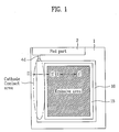
- FIG. 1 illustrates a plane view of an active matrix electroluminescence device according to the present invention
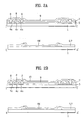
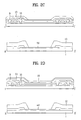
- FIGs. 2A to 2E illustrate cross-sectional views showing the process steps of a method for fabricating the active matrix electroluminescence device according to a first embodiment of the present invention.
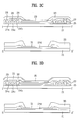
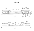
- FIGs. 3A to 3E illustrate cross-sectional views showing the process steps of a method for fabricating the active matrix electroluminescence device according to a second embodiment of the present invention.
- FIG. 1 illustrates a plane view of an active matrix electroluminescence device according to the present invention.
- an emissive area and a non-emissive area are defined on a substrate 1.
- a plurality of emissive pixels is formed in the emissive area.
- a pad part 2 a common electrode contact wire 4d connected to the pad part 2, and circuits, such as a gate driver and a data driver, are formed in the non-emissive area.
- the pixel electrode (i.e. , the ITO layer) and the common electrode (i.e. , cathode) 16 are formed not to be in direct contact with each other, when formed on the wire or the electrode in the non-emissive area.
- FIGs. 2A to 2E illustrate cross-sectional views showing the process steps of a method for fabricating the active matrix electroluminescence device according to a first embodiment of the present invention.
- a metallic material layer is formed on a glass substrate 1, which is then selectively removed.
- the metallic material layer is formed of any one of or an alloy of molybdenum (Mo), aluminum (Al), and neodymium (Nd).
- a gate insulating layer 5 is formed on the entire surface. More specifically, the gate insulating layer 5 is formed on the substrate 1, the source and drain electrodes 4a and 4b, a channel 4c, and the wire 4d. Then, a gate electrode 6 is formed at a predetermined area of the gate insulating layer 5 being aligned with the channel 4c. The source and drain electrodes 4a and 4b, the channel 4c, and the gate electrode 6 form a thin film transistor switching each pixel in the emissive area.
- An interlayer dielectric 7 is formed on the gate insulating layer 5 and the gate electrode 6. Then, the gate insulating layer 5 and the gate electrode 6 are selectively removed, so as to form a plurality of contact holes exposing a portion of the surface of the source and drain electrodes 4a and 4b. At this point, a trench is formed on the gate insulating layer 5 and the interlayer dielectric 7 in the non-emissive area, so as to expose the wire 4d. Thereafter, the contact holes are filled with a metal, thereby forming a plurality of electrode lines 8 each electrically connected to the source and drain electrodes 4a and 4b.
- an insulating material such as a SiN x group material or a SiO x group material, is deposited on the entire surface of the interlayer dielectric 7 and the electrode lines 8, so as to form a protective layer 9.
- the protective layer 9 is selectively removed, thereby exposing the electrode line 8 connected to the drain electrode 4b in the emissive area.
- the protective layer 9 formed on the wire 4d is also removed.
- the gate insulating layer 5, the interlayer dielectric 7, and the protective layer 9 in the non-emissive area can also be etched simultaneously, so as to form the trench exposing the wire 4d.
- the pixel electrode 10 in order to form a pixel electrode 10 in the emissive area, a metallic material is deposited on the protective layer 9, which is then selectively removed.
- the pixel electrode 10 is formed of a transparent material, such as indium tin oxide (ITO).
- the pixel electrode in the top-emission ELD, is formed of a metal having high reflectivity and work function. Since the bottom-emission ELD is given as an example in the present invention, the pixel electrode 10 is formed of an ITO layer.
- the ITO layer 10 is formed only in the pixel area within the emissive area, but the ITO layer 10 is not formed on the wire 4d of the non-emissive area.
- the etchant used for removing the ITO layer 10 deposited on the wire 4d of the non-emissive area However, the etchant used herein should not corrode the substance of the wire 4d.
- an insulating layer 13 is deposited on the entire surface of the protective layer 9 and the pixel electrode 10. Then, the insulating layer 13 is selectively removed, so as to expose a portion of the pixel electrode 10 and the wire 4d.
- the insulating layer 13 forms a boundary area between the pixel areas in the emissive area.
- a shadow mask (not shown) is used to deposit an organic electroluminous layer 15 on the pixel electrode 10.
- the organic electroluminous layer 15 is not formed on the non-emissive layer.
- the organic electroluminescent layer 15 is classified into a red (R) organic electrolumous layer, a green (G) organic electroluminous layer, and a blue (B) organic electroluminous layer depending upon the emitted color. And, the R, G, and B organic electroluminous layers are serially formed in the corresponding pixel area.
- the organic electroluminous includes an organic layer (not shown), a hole injecting layer (not shown) and a hole transport layer (not shown) for injecting and transporting holes supplied from the pixel electrode 10 into the organic layer, respectively, and an electron injecting layer (not shown) and an electron transport layer (not shown) for injecting and transporting electrons supplied from the common electrode into the organic layer, respectively.
- an aluminum (Al) layer or an aluminum alloy layer is deposited on the entire surface of the organic electroluminous layer 15, so as to form the common electrode 16.
- the common electrode 16 is formed on the organic electroluminous layer 15 in the emissive area, and on the wire 4d and the insulating layer 13 in the non-emissive area. Therefore, the common electrode 16 is in direct contact with the wire 4d.
- a protective layer (not shown) is formed, in a later process, so as to protect the organic electroluminous layer 15 from oxygen and moisture. Then, a sealant (not shown) and a transparent substrate are used to form a protective cap.
- FIGs. 3A to 3E illustrate cross-sectional views showing the process steps of a method for fabricating the active matrix electroluminescence device according to a second embodiment of the present invention.
- a metallic material layer is formed on a glass substrate 21, which is then selectively removed.
- the metallic material layer is formed of any one of or an alloy of molybdenum (Mo), aluminum (Al), and neodymium (Nd).
- a gate insulating layer 25 is formed on the entire surface. More specifically, the gate insulating layer 25 is formed on the substrate 21, the source and drain electrodes 24a and 24b, a channel 24c, and the wire 24d. Then, a gate electrode 26 is formed at a predetermined area of the gate insulating layer 25 being aligned with the channel 24c. The source and drain electrodes 24a and 24b, the channel 24c, and the gate electrode 26 form a thin film transistor switching each pixel in the emissive area.
- An interlayer dielectric 27 is formed on the gate insulating layer 25 and the gate electrode 26. Then, the gate insulating layer 25 and the gate electrode 26 are selectively removed, so as to form a plurality of contact holes exposing a portion of the surface of the source and drain electrodes 24a and 24b. At this point, a trench is formed on the interlayer dielectric 27 and the gate insulating layer 25 in the non-emissive area, so as to expose the wire 24d.
- the contact holes are filled with a metal, thereby forming a plurality of electrode lines 28 each electrically connected to the source and drain electrodes 24a and 24b.
- a buffer metal layer 31 is formed on the wire 24d in the non-emissive area. The buffer metal layer 31 is formed either after forming the electrode lines 28 and the protective layer 29, or at the same time the electrode lines 28 are formed. When the buffer electrode layer 31 and the electrode lines 28 are formed simultaneously, the buffer metal layer 31 is formed of the same material as the electrode lines 28.
- the buffer electrode layer 31 is formed of a metal that is not corroded by an ITO etchant, such as any one of chrome (Cr), copper (Cu), tungsten (W), gold (Au), nickel (Ni), silver (Ag), titanium (Ti), tantalum (Ta), or an alloy of any of the same.
- ITO etchant such as any one of chrome (Cr), copper (Cu), tungsten (W), gold (Au), nickel (Ni), silver (Ag), titanium (Ti), tantalum (Ta), or an alloy of any of the same.
- an insulating material such as a SiN x group material or a SiO x group material, is deposited on the entire surface of the gate electrode 26, the interlayer dielectric 27, and the electrode lines 28, so as to form a protective layer 29.
- the protective layer 29 is selectively removed, thereby exposing the electrode line 28 connected to the drain electrode 24b in the emissive area.
- the protective layer 29 is formed after forming the buffer metal layer 31, the protective layer 29 formed on the buffer metal layer 31 is also removed.
- an ITO layer is formed on the protective layer 29 in order to form the pixel electrode 30 in the emissive area, and then, the ITO layer is selectively removed.
- the etchant used to remove the ITO layer 30, which is deposited in the non-emissive area, may be corrosive to the material of the wire 24d. Since the buffer metal layer 31 is formed on the wire 24d, the buffer metal layer 31 can protect the wire 24d from corrosion.
- the ITO layer 30 is formed only in the pixel area within the emissive area and is not formed in the non-emissive area.
- the insulating layer 33 is selectively removed so as to expose a portion of the pixel electrode 30 and the buffer metal layer 31.
- the insulating layer 33 forms a boundary area between the pixel areas in the emissive area.
- a shadow mask (not shown) is used to deposit an organic electroluminous layer 35 on the pixel electrode 30. At this point, the organic electroluminous layer 35 is not formed on the non-emissive layer.
- a common electrode 36 is formed on the entire surface of the organic electroluminous layer 35.
- the common electrode 36 is formed on the organic electroluminous layer 35 in the emissive area, and on the buffer metal layer 31 and the insulating layer 33 in the non-emissive area. Accordingly, the common electrode 36 is not in direct contact with the wire 24d. Instead, the common electrode 36 is electrically connected to the wire 24d through the buffer metal layer 31.
- a protective layer (not shown) is formed, in a later process, so as to protect the organic electroluminous layer 35 from oxygen and moisture. Then, a sealant (not shown) and a transparent substrate are used to form a protective cap.
- the ITO layer is not formed on the wire or electrode that contacts the common electrode from the outside of the emissive layer, or, alternatively, another metal layer is formed instead of the ITO layer, thereby preventing changes in the interfacial characteristic caused by the ITO layer.
Landscapes
- Engineering & Computer Science (AREA)
- Microelectronics & Electronic Packaging (AREA)
- Manufacturing & Machinery (AREA)
- Electroluminescent Light Sources (AREA)
- Devices For Indicating Variable Information By Combining Individual Elements (AREA)
Priority Applications (2)
| Application Number | Priority Date | Filing Date | Title |
|---|---|---|---|
| EP09178265A EP2161753A3 (de) | 2003-09-08 | 2004-08-12 | Elektrolumineszenzvorrichtung mit aktiver Matrix und Herstellungsverfahren dafür |
| EP16173259.9A EP3098856B1 (de) | 2003-09-08 | 2004-08-12 | Elektrolumineszenzvorrichtung mit aktiver matrix und verfahren zur herstellung davon |
Applications Claiming Priority (2)
| Application Number | Priority Date | Filing Date | Title |
|---|---|---|---|
| KR2003062622 | 2003-09-08 | ||
| KR1020030062622A KR100546668B1 (ko) | 2003-09-08 | 2003-09-08 | 유기 el 디스플레이 패널 제조 방법 |
Related Child Applications (1)
| Application Number | Title | Priority Date | Filing Date |
|---|---|---|---|
| EP16173259.9A Division EP3098856B1 (de) | 2003-09-08 | 2004-08-12 | Elektrolumineszenzvorrichtung mit aktiver matrix und verfahren zur herstellung davon |
Publications (2)
| Publication Number | Publication Date |
|---|---|
| EP1513196A2 true EP1513196A2 (de) | 2005-03-09 |
| EP1513196A3 EP1513196A3 (de) | 2006-06-07 |
Family
ID=34132241
Family Applications (3)
| Application Number | Title | Priority Date | Filing Date |
|---|---|---|---|
| EP16173259.9A Expired - Lifetime EP3098856B1 (de) | 2003-09-08 | 2004-08-12 | Elektrolumineszenzvorrichtung mit aktiver matrix und verfahren zur herstellung davon |
| EP04019148A Ceased EP1513196A3 (de) | 2003-09-08 | 2004-08-12 | Elektrolumineszierende Anzeigevorrichtungen mit aktiver Matrix und deren Herstellungsverfahren |
| EP09178265A Ceased EP2161753A3 (de) | 2003-09-08 | 2004-08-12 | Elektrolumineszenzvorrichtung mit aktiver Matrix und Herstellungsverfahren dafür |
Family Applications Before (1)
| Application Number | Title | Priority Date | Filing Date |
|---|---|---|---|
| EP16173259.9A Expired - Lifetime EP3098856B1 (de) | 2003-09-08 | 2004-08-12 | Elektrolumineszenzvorrichtung mit aktiver matrix und verfahren zur herstellung davon |
Family Applications After (1)
| Application Number | Title | Priority Date | Filing Date |
|---|---|---|---|
| EP09178265A Ceased EP2161753A3 (de) | 2003-09-08 | 2004-08-12 | Elektrolumineszenzvorrichtung mit aktiver Matrix und Herstellungsverfahren dafür |
Country Status (5)
| Country | Link |
|---|---|
| US (2) | US7518308B2 (de) |
| EP (3) | EP3098856B1 (de) |
| JP (3) | JP4702519B2 (de) |
| KR (1) | KR100546668B1 (de) |
| CN (1) | CN100536193C (de) |
Cited By (1)
| Publication number | Priority date | Publication date | Assignee | Title |
|---|---|---|---|---|
| EP2061083A1 (de) | 2007-11-16 | 2009-05-20 | Samsung Mobile Display Co., Ltd. | Organische lichtemittierende Vorrichtung |
Families Citing this family (5)
| Publication number | Priority date | Publication date | Assignee | Title |
|---|---|---|---|---|
| KR100782457B1 (ko) | 2005-10-20 | 2007-12-05 | 삼성에스디아이 주식회사 | 유기전계 발광표시장치 |
| US8026513B2 (en) * | 2006-01-05 | 2011-09-27 | Konica Minolta Holdings, Inc. | Bottom emission type organic electroluminescent panel |
| KR101764272B1 (ko) | 2010-12-02 | 2017-08-16 | 삼성디스플레이 주식회사 | 유기 발광 표시 장치 및 그 제조방법 |
| KR101802523B1 (ko) * | 2011-08-02 | 2017-11-28 | 엘지디스플레이 주식회사 | 유기전계발광표시장치와 이의 제조방법 |
| KR102568518B1 (ko) * | 2016-10-25 | 2023-08-18 | 엘지디스플레이 주식회사 | 고 개구율을 갖는 초고해상도 평판 표시장치 |
Citations (2)
| Publication number | Priority date | Publication date | Assignee | Title |
|---|---|---|---|---|
| US5999235A (en) * | 1996-12-17 | 1999-12-07 | Mitsubishi Denki Kabushiki Kaisha | Liquid crystal displaying apparatus and method of manufacturing TFT array |
| WO2003005773A1 (en) * | 2001-05-25 | 2003-01-16 | Samsung Electronics Co., Ltd. | Organic electroluminescence device and method for fabricating thereof |
Family Cites Families (18)
| Publication number | Priority date | Publication date | Assignee | Title |
|---|---|---|---|---|
| JP3306923B2 (ja) | 1992-10-09 | 2002-07-24 | セイコーエプソン株式会社 | 液晶装置の製造方法 |
| JPH06337440A (ja) | 1993-05-28 | 1994-12-06 | Seiko Epson Corp | Mim型非線形素子及びその製造方法 |
| JP3097841B2 (ja) * | 1997-11-20 | 2000-10-10 | 松下電器産業株式会社 | フォトマスク及びアクティブ素子アレイ基板の製造方法 |
| JP3423232B2 (ja) * | 1998-11-30 | 2003-07-07 | 三洋電機株式会社 | アクティブ型el表示装置 |
| JP3346324B2 (ja) | 1999-02-26 | 2002-11-18 | 日本電気株式会社 | エッチング方法 |
| JP4075028B2 (ja) * | 1999-06-14 | 2008-04-16 | セイコーエプソン株式会社 | 回路基板、表示装置、および電子機器 |
| JP2001102169A (ja) * | 1999-10-01 | 2001-04-13 | Sanyo Electric Co Ltd | El表示装置 |
| JP2001281698A (ja) | 2000-03-30 | 2001-10-10 | Advanced Display Inc | 電気光学素子の製法 |
| TW493282B (en) | 2000-04-17 | 2002-07-01 | Semiconductor Energy Lab | Self-luminous device and electric machine using the same |
| JP2001337619A (ja) * | 2000-05-25 | 2001-12-07 | Toshiba Corp | アレイ基板の製造方法 |
| KR100715943B1 (ko) * | 2001-01-29 | 2007-05-08 | 삼성전자주식회사 | 액정표시장치 및 그 제조방법 |
| JP3608614B2 (ja) | 2001-03-28 | 2005-01-12 | 株式会社日立製作所 | 表示装置 |
| KR100600844B1 (ko) | 2001-04-04 | 2006-07-14 | 삼성에스디아이 주식회사 | 유기 전계 발광 표시장치의 제조 방법 |
| JP2003059939A (ja) * | 2001-08-08 | 2003-02-28 | Advanced Display Inc | 薄膜トランジスタアレイ基板およびその製造方法 |
| KR100743105B1 (ko) | 2001-10-22 | 2007-07-27 | 엘지.필립스 엘시디 주식회사 | 유기 전계발광표시소자 및 그 제조방법 |
| US7042024B2 (en) | 2001-11-09 | 2006-05-09 | Semiconductor Energy Laboratory Co., Ltd. | Light emitting apparatus and method for manufacturing the same |
| TW582182B (en) * | 2003-02-19 | 2004-04-01 | Au Optronics Corp | AM-OLED display |
| US7057208B2 (en) * | 2003-03-25 | 2006-06-06 | Semiconductor Energy Laboratory Co., Ltd. | Display device and manufacturing method thereof |
-
2003
- 2003-09-08 KR KR1020030062622A patent/KR100546668B1/ko not_active Expired - Fee Related
-
2004
- 2004-07-29 JP JP2004221860A patent/JP4702519B2/ja not_active Expired - Fee Related
- 2004-07-30 US US10/902,066 patent/US7518308B2/en not_active Expired - Fee Related
- 2004-08-12 EP EP16173259.9A patent/EP3098856B1/de not_active Expired - Lifetime
- 2004-08-12 EP EP04019148A patent/EP1513196A3/de not_active Ceased
- 2004-08-12 EP EP09178265A patent/EP2161753A3/de not_active Ceased
- 2004-08-20 CN CNB200410064151XA patent/CN100536193C/zh not_active Expired - Fee Related
-
2009
- 2009-02-17 US US12/372,463 patent/US8310151B2/en not_active Expired - Fee Related
-
2010
- 2010-02-16 JP JP2010031663A patent/JP5083677B2/ja not_active Expired - Fee Related
- 2010-10-18 JP JP2010233543A patent/JP5413745B2/ja not_active Expired - Fee Related
Patent Citations (2)
| Publication number | Priority date | Publication date | Assignee | Title |
|---|---|---|---|---|
| US5999235A (en) * | 1996-12-17 | 1999-12-07 | Mitsubishi Denki Kabushiki Kaisha | Liquid crystal displaying apparatus and method of manufacturing TFT array |
| WO2003005773A1 (en) * | 2001-05-25 | 2003-01-16 | Samsung Electronics Co., Ltd. | Organic electroluminescence device and method for fabricating thereof |
Cited By (2)
| Publication number | Priority date | Publication date | Assignee | Title |
|---|---|---|---|---|
| EP2061083A1 (de) | 2007-11-16 | 2009-05-20 | Samsung Mobile Display Co., Ltd. | Organische lichtemittierende Vorrichtung |
| US8030838B2 (en) | 2007-11-16 | 2011-10-04 | Samsung Mobile Display Co., Ltd. | Organic light emitting display apparatus |
Also Published As
| Publication number | Publication date |
|---|---|
| JP5413745B2 (ja) | 2014-02-12 |
| US20050052126A1 (en) | 2005-03-10 |
| JP4702519B2 (ja) | 2011-06-15 |
| CN100536193C (zh) | 2009-09-02 |
| EP3098856A1 (de) | 2016-11-30 |
| EP3098856B1 (de) | 2022-04-06 |
| KR20050025786A (ko) | 2005-03-14 |
| EP1513196A3 (de) | 2006-06-07 |
| US8310151B2 (en) | 2012-11-13 |
| JP2011100120A (ja) | 2011-05-19 |
| JP5083677B2 (ja) | 2012-11-28 |
| EP2161753A3 (de) | 2010-07-14 |
| JP2010153388A (ja) | 2010-07-08 |
| JP2005084675A (ja) | 2005-03-31 |
| CN1596039A (zh) | 2005-03-16 |
| KR100546668B1 (ko) | 2006-01-26 |
| US20090153047A1 (en) | 2009-06-18 |
| US7518308B2 (en) | 2009-04-14 |
| EP2161753A2 (de) | 2010-03-10 |
Similar Documents
| Publication | Publication Date | Title |
|---|---|---|
| US7312571B2 (en) | Organic electroluminescent device including layer having uneven patterns | |
| US7755280B2 (en) | Active matrix electroluminescence device having a metallic protective layer and method for fabricating the same | |
| US7803029B2 (en) | Method of fabricating organic electroluminescent display device | |
| US7804242B2 (en) | Top-emission active matrix electroluminescence device and method for fabricating the same | |
| CN102222683A (zh) | 平板显示器设备及其制造方法 | |
| US20080136339A1 (en) | Organic EL display device | |
| US8310151B2 (en) | Active matrix electroluminescence device and method for fabricating the same | |
| KR100556369B1 (ko) | 유기 el 소자 및 그 제조 방법 | |
| KR20100065685A (ko) | 듀얼패널 타입 유기전계 발광소자 및 이의 제조 방법 | |
| KR20080104452A (ko) | 유기전계 발광소자 및 그 제조 방법 | |
| KR20090031149A (ko) | 전계발광소자 |
Legal Events
| Date | Code | Title | Description |
|---|---|---|---|
| PUAI | Public reference made under article 153(3) epc to a published international application that has entered the european phase |
Free format text: ORIGINAL CODE: 0009012 |
|
| AK | Designated contracting states |
Kind code of ref document: A2 Designated state(s): AT BE BG CH CY CZ DE DK EE ES FI FR GB GR HU IE IT LI LU MC NL PL PT RO SE SI SK TR |
|
| AX | Request for extension of the european patent |
Extension state: AL HR LT LV MK |
|
| PUAL | Search report despatched |
Free format text: ORIGINAL CODE: 0009013 |
|
| AK | Designated contracting states |
Kind code of ref document: A3 Designated state(s): AT BE BG CH CY CZ DE DK EE ES FI FR GB GR HU IE IT LI LU MC NL PL PT RO SE SI SK TR |
|
| AX | Request for extension of the european patent |
Extension state: AL HR LT LV MK |
|
| 17P | Request for examination filed |
Effective date: 20061005 |
|
| 17Q | First examination report despatched |
Effective date: 20061117 |
|
| AKX | Designation fees paid |
Designated state(s): DE FR GB NL |
|
| STAA | Information on the status of an ep patent application or granted ep patent |
Free format text: STATUS: THE APPLICATION HAS BEEN REFUSED |
|
| 18R | Application refused |
Effective date: 20130629 |