EP1511176B1 - Méthode et appareil pour digitaliser plusieurs signaux analogiques en parallèle - Google Patents
Méthode et appareil pour digitaliser plusieurs signaux analogiques en parallèle Download PDFInfo
- Publication number
- EP1511176B1 EP1511176B1 EP20040103965 EP04103965A EP1511176B1 EP 1511176 B1 EP1511176 B1 EP 1511176B1 EP 20040103965 EP20040103965 EP 20040103965 EP 04103965 A EP04103965 A EP 04103965A EP 1511176 B1 EP1511176 B1 EP 1511176B1
- Authority
- EP
- European Patent Office
- Prior art keywords
- signal
- unit
- rate
- digital
- sampling
- Prior art date
- Legal status (The legal status is an assumption and is not a legal conclusion. Google has not performed a legal analysis and makes no representation as to the accuracy of the status listed.)
- Expired - Fee Related
Links
Images

Classifications
-
- H—ELECTRICITY
- H03—ELECTRONIC CIRCUITRY
- H03M—CODING; DECODING; CODE CONVERSION IN GENERAL
- H03M1/00—Analogue/digital conversion; Digital/analogue conversion
- H03M1/12—Analogue/digital converters
- H03M1/1205—Multiplexed conversion systems
- H03M1/122—Shared using a single converter or a part thereof for multiple channels, e.g. a residue amplifier for multiple stages
- H03M1/1225—Shared using a single converter or a part thereof for multiple channels, e.g. a residue amplifier for multiple stages using time-division multiplexing
Definitions
- the present invention relates to a device and a method for the device for converting at least two parallel incoming analog signals to be processed by digital signal processors digital signals, wherein at least a first analog signal of the incoming analog signals at least one first signal path is assignable and at least one further, in particular at least one second , Analog signal of the incoming analog signals at least one further, in particular at least one second signal path is assignable.
- a [nalog] / D [igital] converters are an indispensable part of modern communication systems; however, analog-to-digital converters, with their high technical requirements and specifications, represent a significant cost factor gaining in importance as digital logic progresses in miniaturization. This cost factor is particularly evident in broadcast receivers, where it is often desirable to receive multiple systems simultaneously, so that conventionally a corresponding number of analog-to-digital converters are needed.
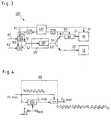
- the first, in Figure 1 upper analog signal A1 passes through a sampling unit P1, which is clocked by a clock generator unit T1. Subsequently, the sampled values of the sampled analog signal A1 are digitized in a quantization unit Q1 connected downstream of the sampling unit P1 and further processed in a digital signal processor 10 connected downstream of the quantization unit Q1; The same applies to the second, in Figure 1 lower analog signal A2 as well as possibly for further, simultaneously with the first analog signal A1 and the second analog signal A2 arriving further analog signals.
- a device for converting at least two parallel incoming analog signals to digital signals to be processed by means of digital signal processors.
- the two parallel incoming analog signals are assigned to two different signal paths in which they are simultaneously convertible by means of an analog / digital converter. There is a sampling of the incoming analog signals in response to a clock signal at different time intervals.
- the present invention has the object, a device of the type mentioned and a method of the type mentioned so that the size and cost of the device or implementation of the method are minimized.
- sampling rate which is also referred to as the sampling frequency
- sampling frequency is the frequency at which instantaneous voltage samples are taken as samples from the analog input signal.
- the quantization unit associated with the analog-to-digital converter operates at a double rate compared to single systems known from the prior art.
- the quantization unit is alternately assigned to one or the other system defined by the respective channel or signal path, so that a two-channel quantizer with a symmetrical sampling rate is formed.
- sampling frequency or sampling rate indicates how many times in one second the analog-to-digital converter determines a sample from the incoming analog signal.
- the sampling frequency or sampling rate is critical to the quality of the A [nalog] / D [igital] conversion; For example, in sound cards, sampling rates of about four kilohertz to about 44 kilohertz are common; In the studio area, sampling frequencies of up to 96 kilohertz and above are used (24-bit converters to 36-bit converters).
- the above principle can be implemented not only for two but also for N (> 2) channels or paths, with all paths or systems being operated with the same sampling clock; in this case, then an N-channel quantizer with symmetrical sampling rate formed.
- the symmetrical variant of the present invention should usefully be used for two substantially similar analog input signals with similar or equal frequency bandwidth, it is advisable to use the asymmetrical variant of the present invention for the case where the first analog input signal has a higher frequency bandwidth than the further analog Input signal (or as the other analog input signals), because for this (s) narrow-band (s) analog signal (s) satisfies a lower sampling rate than for the first analog signal.
- the output signal of the quantization unit assigned to the analog / digital converter, in particular integrated in the analog / digital converter, is supplied to the digital signal processing paths. Since the first path continues to run at the full sampling rate, every Nth value (in the above example: every fifth value) but is assigned to the second path, the sampled and then quantized first signal must be added, since every Nth value ( in the above example: every fifth value) of the first signal is missing:
- Such a supplementing of the quantized first signal is possible via an adapted to this quantized first signal interpolation, which is associated with a certain implementation effort, in particular with a certain amount of computation.
- An even more advantageous variant of the signal supplement is to replace the missing samples in the first channel or signal path by zero, that is, by a vanishing sample.
- the sampling rate In order to reproduce the original signal from the sampled voltage values, the sampling rate must be at least twice the sampling rate of the sampled signal. For example, if the signal to be sampled has a frequency of 500 kilohertz, then the sampling rate must be one megahertz or more.
- sampling theorem is fundamental to the application of information theory to continuous signals because it allows the representation of a continuous signal of finite duration by a finite number of degrees of freedom, that is also as a binary signal.
- the results of signal processing thus remain Usually unadulterated, because in broadcast applications only the desired channel with the desired program is selected.
- the present invention further relates to a circuit arrangement, in particular an integrated circuit, comprising a device according to the kind set forth above.
- the present invention relates to the use of at least one device according to the kind set out above and / or at least one circuit arrangement according to the kind set out above and / or a method according to the kind set out above in digital communication systems, in particular in digital broadcast receiving systems.
- D [igital] S [ignal] P [rocessor] s the D [igital] S [ignal] P [rocessor] s 10, 12 to electronic component for processing the digitized audio signals according to a predetermined algorithm, with an override of the digital signal processors 10, 12 is to be avoided if possible.
- the peculiarity of the first exemplary embodiment according to FIG. 2 and of the second exemplary embodiment according to FIG. 3 can be seen in that the two analog signals A1, A2 are generated by means of a single analogue / digital converter 20 (see FIG 20 '(see Figure 3) can be digitized simultaneously.
- analog signals are first sampled in a time frame (sampling theorem), then quantified and encoded in a dual system.
- Analog / digital converters basically work according to different conversion methods, which differ in the conversion speed, the quantization, the coding and the resolution with which the analog signals are digitally reproduced.
- the conversion of the analog signals into the digital signals is necessary to allow processing of the binary signal by a computer or by the digital signal processors 10, 12.
- In the domestic sector are currently predominantly 16-bit converters used in the professional field 20-bit converters to 36-bit converters.
- the first analog signal A1 in FIG. 2 and the second analog signal A2 lower in FIG. 2 are received symmetrically and alternately by means of a sampling rate R sampled by respective samples.
- the clock for this symmetrical sampling of the two signal paths S1, S2 is provided by a clock unit 40, which applies the sampling rate R to the analog / digital converter 20, and here in particular the first signal path S1 and the second signal path S2.
- the second analog signal A2 lower in FIG. 3 is sampled in a second sampling unit 32 connected in parallel with the analog / digital converter 20 'and connected in parallel with the first sampling unit 30 to obtain second sampling values, the sampling unit 32 being triggered by the second sampling clock R2 supplied by the clock unit 40 'and after passing through the frequency divider unit 42' corresponds to a rational fraction of the first sample clock R1.
- a sampling and quantization distributed to the two channels S1, S2 is given insofar as the time intervals defined by the sampling rate R2 of the second signal path S2 during which the first signal path S1 is not sampled or quantized is used to sample or quantize the second signal path S2.
- a peculiarity of the second embodiment according to FIG. 3 can therefore be seen in the fact that in the first signal path S1 every fifth value is not sampled, because in this time interval the second signal path S2 is being sampled. In other words, of the samples of the first signal A1, every fifth value due to non-sampling is missing and therefore to be replaced or supplemented.
- This replacement or supplementation is realized by means of a signal supplementing unit 60 which is arranged in the first signal path S 1 between the quantization unit 50 'and the first digital signal processor 10.
- the replacement takes place by replacing the missing fifth values of the first digital signal Z1 formed in the quantization unit 50 'with a vanishing sample, namely zero.
- the sampling rate is dependent on the frequency of the signal to be sampled and is subject to the sampling theorem, according to which signal reproduction presupposes a sampling rate which is at least twice as high as the frequency of the signal to be sampled.
- the temporal correlation between the sampling of the second signal path S2 and the signal supplement 60 connected downstream of the quantization unit 50 'in the first signal path S1 is given by the clock unit 40' and by the further frequency divider units 42 'connected downstream of the clock unit 40'; Specifically, in the second embodiment shown in FIG. 3, the sampling of the second analog signal A2 by the rates R2 obtained by the frequency divider units 42 'is time correlated with the replacement of each fifth value of the first digitized signal Z1.
- the supplemented and thus "complete" first digital signal Z1 is finally further processed in the first digital signal processor 10; the further digital signal Z2 likewise formed in the quantization unit 50 'is further processed in the second digital signal processor 12.
- the fact that the power consumption of an analogue-to-digital converter unit basically increases in an approximately proportional manner to the sampling rate must be considered.
- any Nth value of the quantized signal Z1: x (n) received by the quantizer 50 '(see Fig. 3) is replaced with zero, that is, with a zero value.
Landscapes
- Engineering & Computer Science (AREA)
- Theoretical Computer Science (AREA)
- Analogue/Digital Conversion (AREA)
Claims (6)
- Dispositif (100, 100') pour convertir au moins deux signaux analogiques d'entrée (A1, A2) par des processeurs numériques de signaux (10, 12) pour obtenir des signaux numériques à traiter (Z1, Z2),- au moins un premier signal analogique (A1) des signaux analogiques d'entrée (A1, A2) étant associé à au moins un premier chemin de signal (S1) et au moins un autre, notamment au moins un second signal analogique (A2) des signaux analogiques d'entrée (A1, A2) étant associé à au moins un autre, notamment au moins un second chemin de signal (S2),- au moins les deux signaux analogiques (A1, A2) étant convertis en même temps par un convertisseur analogique/numérique (20, 20'),- au moins une unité de détection (22 ; 30, 32) détectant les signaux analogiques respectifs (A1, A2) pour obtenir les valeurs de détection respectives, le premier chemin de signal (S1) et l'autre notamment le second chemin de signal (S2), fonctionnant avec chaque fois une vitesse (R, R1, R2) notamment une vitesse de détection générée par au moins une unité d'horloge (40, 40'),- le convertisseur analogique/numérique (20, 20') ayant une unité de quantification (50, 50') en aval de l'unité de détection (22 ; 30, 32), cette unité de quantification étant associée selon les valeurs de détection à quantifier respectivement suivant la vitesse (R) notamment les vitesses de détection ou selon les vitesses (R1, R2) notamment les vitesses de détection à au moins deux chemins de signal (S1, S2),caractérisé en ce que
la vitesse (R2) notamment la vitesse de détection de l'autre chemin de signal (S2), notamment du second chemin de signal, correspond à une fraction notamment la fraction rationnelle (1/N) de la vitesse (R1) notamment de la vitesse de détection du premier chemin de signal (S1), fraction fournie par au moins une unité de division (42'), notamment par au moins une unité de division de fréquence. - Dispositif selon la revendication 1,
caractérisé en ce qu'
au moins une unité de complément de signal (60) est prévue dans le premier chemin de signal (S1),- à l'aide de l'unité de complément de signal (60), on remplace les valeurs manquantes par non détection notamment on remplace le zéro, et- on complète notamment par des valeurs d'interpolation, la corrélation dans le temps entre la détection de l'autre chemin notamment du second chemin de signal (S2) et notamment de l'unité de complément de signal (60) en aval de l'unité de quantification (50') sont données par l'unité d'horloge (40') et par au moins une autre unité de division (42') qui applique la vitesse (R2) à l'unité de complément de signal (60), et- dans les intervalles de temps définis par la vitesse (R2) notamment la vitesse de détection de l'autre chemin de signal (S2) notamment du second chemin de signal, pendant lesquels le premier chemin de signal (S1) n'est pas détecté, on détecte l'autre chemin de signal (S2) notamment le second chemin de signal. - Circuit notamment circuit intégré comportant un dispositif (100, 100'),
selon l'une quelconque des revendications 1 ou 2. - Procédé de conversion d'au moins deux signaux analogiques entrant (A1, A2), parallèles, par des processeurs numériques de signaux (10, 12) pour obtenir des signaux numériques (Z1, Z2) à traiter,
au moins un premier signal analogique (A1) parmi les signaux analogiques entrant (A1, A2) étant associés à au moins un premier chemin de signal (S1) et au moins un autre signal analogique (A2) notamment au moins un second signal analogique parmi les signaux analogiques entrant (A1, A2) étant appliqués à au moins un autre chemin de signal (S2), notamment à au moins un second chemin de signal (S2), et- au moins les deux signaux analogiques (A1, A2) sont convertis simultanément par un convertisseur analogique/numérique (20, 20'),- le premier signal analogique (A1) étant détecté dans une première unité de détection (30) selon une première vitesse (R1) notamment à une première vitesse de détection pour obtenir les premières valeurs de détection, et l'autre signal analogique (A2), notamment le second signal analogique est détecté dans au moins une autre unité de détection (32) notamment au moins une seconde unité de détection (32) avec une autre vitesse (R2) notamment une seconde vitesse, notamment la vitesse de détection pour obtenir d'autres valeurs de détection notamment des secondes valeurs de détection, et- dans une unité de quantification (50) pour tous les chemins de signal (S1, S2), on quantifie les valeurs de détection sous la forme de signaux numériques (Z1, Z2), et- les signaux numériques (Z1, Z2) sont traités dans les processeurs numériques de signaux respectifs (10, 12), notamment on poursuit leur traitement,caractérisé en ce qu'- on choisit la vitesse (2), notamment la vitesse de détection de l'autre chemin de signal (S2) notamment du second chemin de signal de façon à correspondre à une fraction de la vitesse (R1) notamment de la vitesse de détection du premier chemin de signal (S1). - Procédé selon la revendication 4,
caractérisé en ce que
l'autre vitesse (R2) notamment la seconde vitesse correspond notamment à une fraction rationnelle (1/N) de la première vitesse (R1) de façon que les intervalles de temps définis par l'autre vitesse (R2) notamment la seconde vitesse (R2) soit utilisés pour détecter l'autre signal analogique (A2), notamment le second signal analogique pendant que le premier signal analogique (A1) n'est pas détecté,- dans une unité de quantification (50') on quantifie les premières valeurs de détection ainsi que les autres valeurs de détection notamment les secondes,- les valeurs manquantes par non détection dans le premier signal numérique (Z1 : x(n)) formées dans l'unité de quantification (50'), sont remplacées par au moins une unité de complément de signal (60) en formant un premier signal numérique complet (Z1 : y(n)),- on remplace notamment par zéro, ou- on complète notamment par des valeurs interpolées, et
la détection de l'autre signal analogique (A2) notamment du second signal analogique et le complément de signal du premier signal numérique (Z1), notamment par l'unité de quantification (50') en aval, est mise en corrélation de temps par au moins une unité d'horloge (40') et par au moins une autre unité de division (42') appliquant la vitesse (R2) à l'unité de complément de signal (60),- le premier signal numérique complet (Z1; y(n)) étant traité dans le premier processeur de signal numérique (10) notamment son traitement étant poursuivi, et- l'autre signal numérique (Z2) notamment le second signal numérique formé dans l'unité de quantification (50'), est traité ensuite notamment son traitement est poursuivi dans le second processeur numérique de signal (12),les résultats du traitement du premier signal numérique (Z1) n'étant pas influencés dans le cas où les valeurs manquantes sont remplacées par zéro, si pour les signaux analogiques (A1, A2) on utilise chaque fois selon une partie de l'ensemble de la largeur de bande de fréquence. - Utilisation d'au moins un dispositif (100, 100') selon au moins 'l'une quelconque des revendications 1 ou 2 et/ ou au moins un circuit selon la revendication 3 et/ou un procédé selon l'une quelconque des revendications 4 ou 5 dans les systèmes de communication numérique notamment des systèmes numériques de réception radio.
Applications Claiming Priority (2)
| Application Number | Priority Date | Filing Date | Title |
|---|---|---|---|
| DE10339644 | 2003-08-28 | ||
| DE2003139644 DE10339644A1 (de) | 2003-08-28 | 2003-08-28 | Vorrichtung sowie Verfahren zum Digitalisieren von parallel eingehenden Analogsignalen |
Publications (2)
| Publication Number | Publication Date |
|---|---|
| EP1511176A1 EP1511176A1 (fr) | 2005-03-02 |
| EP1511176B1 true EP1511176B1 (fr) | 2007-11-14 |
Family
ID=34089233
Family Applications (1)
| Application Number | Title | Priority Date | Filing Date |
|---|---|---|---|
| EP20040103965 Expired - Fee Related EP1511176B1 (fr) | 2003-08-28 | 2004-08-18 | Méthode et appareil pour digitaliser plusieurs signaux analogiques en parallèle |
Country Status (2)
| Country | Link |
|---|---|
| EP (1) | EP1511176B1 (fr) |
| DE (2) | DE10339644A1 (fr) |
Family Cites Families (3)
| Publication number | Priority date | Publication date | Assignee | Title |
|---|---|---|---|---|
| US6486809B1 (en) * | 1999-06-02 | 2002-11-26 | Texas Instruments Incorporated | Analog to digital converter with configurable sequence controller |
| DE10042959C1 (de) * | 2000-08-31 | 2002-01-03 | Siemens Ag | Verfahren und Anordnung zur gleichzeitigen Analog-Digital-Wandlung mehrerer analoger Signale |
| CN100527802C (zh) * | 2001-12-11 | 2009-08-12 | 汤姆森许可公司 | 用于复用的模数转换的系统和方法 |
-
2003
- 2003-08-28 DE DE2003139644 patent/DE10339644A1/de not_active Withdrawn
-
2004
- 2004-08-18 DE DE200450005474 patent/DE502004005474D1/de active Active
- 2004-08-18 EP EP20040103965 patent/EP1511176B1/fr not_active Expired - Fee Related
Also Published As
| Publication number | Publication date |
|---|---|
| EP1511176A1 (fr) | 2005-03-02 |
| DE10339644A1 (de) | 2005-03-24 |
| DE502004005474D1 (de) | 2007-12-27 |
Similar Documents
| Publication | Publication Date | Title |
|---|---|---|
| DE602004012620T2 (de) | Digitalisiereranordnung | |
| EP0497115B1 (fr) | Procédé de shuntage des interruptions de signaux audio | |
| EP0080014A2 (fr) | Démodulateur numérique pour signaux modulés en fréquence | |
| DE102012217582A1 (de) | Kalibrierung eines rekonstruierten Signals unter Anwendung eines Mehrton-Kalibriersignals | |
| DE102013207464A1 (de) | Messverfahren und Messgerät zur Vermessung von breitbandigen Messsignalen | |
| EP0321681B1 (fr) | Partie d'un téléviseur avec des étages opérant numériquement | |
| DE102012100460A1 (de) | Prüfanordnung und Prüfverfahren zur zerstörungsfreien Erfassung eines Fehlers in einem Prüfling mittels eines Wirbelstroms | |
| DE102021209433A1 (de) | Signalempfänger, der Digitalbildsignaltrennung umfasst | |
| DE60310535T2 (de) | System zum Anpassen von Digitalisierern in verzahnten Systemen | |
| DE19625855C2 (de) | Verfahren und Signalauswerteeinrichtung zur Datenreduktion bei der Verarbeitung von Signalwerten mit einer digitalen Signalverarbeitungseinheit in einem Übertragungssystem | |
| EP1511176B1 (fr) | Méthode et appareil pour digitaliser plusieurs signaux analogiques en parallèle | |
| EP2958242B1 (fr) | Dispositif et procédé de traitement d'un signal radio | |
| DE102004049348A1 (de) | Verfahren sowie Einrichtung zur Kompensation von Kennlinienfehlern eines Analog-Digital-Wandlers | |
| EP2060036A1 (fr) | Dispositif et procédé d'analyse d'un signal de mesure transmis par un système multicanal | |
| WO1989003574A1 (fr) | Procede de codage numerique adaptatif par transformees | |
| DE10360470B4 (de) | Verfahren und Vorrichtung zum Demodulieren eines Empfangssignals | |
| WO2006034681A1 (fr) | Procede et dispositif d'essai pour tester des convertisseurs analogiques-numeriques | |
| EP2070189A1 (fr) | Récepteur radio | |
| EP2706363A2 (fr) | Ligne de marquage des points temporels communs | |
| DE10005605B4 (de) | Analoge Vorstufe | |
| EP2659281B1 (fr) | Procédé et dispositif servant à augmenter la précision de repérage radiogoniométrique d'un système de réception | |
| EP0319851A1 (fr) | Commande de phase numérique pour signaux engendrés numériquement | |
| DE102012210498A1 (de) | Signalmessgerät, Signalmessverfahren und Programm | |
| DE19800775C2 (de) | Verfahren und Anordnung zum Reduzieren der Linearitätsfehlereinflüsse bei Hochfrequenzschaltungen, inbesondere AD-Wandler | |
| DE60016633T2 (de) | Verfahren und anordnung zur analog/digital-wandlung eines signals mit einer niederfrequenz-komponente |
Legal Events
| Date | Code | Title | Description |
|---|---|---|---|
| PUAI | Public reference made under article 153(3) epc to a published international application that has entered the european phase |
Free format text: ORIGINAL CODE: 0009012 |
|
| AK | Designated contracting states |
Kind code of ref document: A1 Designated state(s): AT BE BG CH CY CZ DE DK EE ES FI FR GB GR HU IE IT LI LU MC NL PL PT RO SE SI SK TR |
|
| AX | Request for extension of the european patent |
Extension state: AL HR LT LV MK |
|
| 17P | Request for examination filed |
Effective date: 20050902 |
|
| AKX | Designation fees paid |
Designated state(s): DE FR GB IT |
|
| 17Q | First examination report despatched |
Effective date: 20051223 |
|
| GRAP | Despatch of communication of intention to grant a patent |
Free format text: ORIGINAL CODE: EPIDOSNIGR1 |
|
| GRAS | Grant fee paid |
Free format text: ORIGINAL CODE: EPIDOSNIGR3 |
|
| GRAA | (expected) grant |
Free format text: ORIGINAL CODE: 0009210 |
|
| AK | Designated contracting states |
Kind code of ref document: B1 Designated state(s): DE FR GB IT |
|
| REG | Reference to a national code |
Ref country code: GB Ref legal event code: FG4D Free format text: NOT ENGLISH |
|
| REF | Corresponds to: |
Ref document number: 502004005474 Country of ref document: DE Date of ref document: 20071227 Kind code of ref document: P |
|
| GBT | Gb: translation of ep patent filed (gb section 77(6)(a)/1977) |
Effective date: 20080225 |
|
| ET | Fr: translation filed | ||
| PLBE | No opposition filed within time limit |
Free format text: ORIGINAL CODE: 0009261 |
|
| STAA | Information on the status of an ep patent application or granted ep patent |
Free format text: STATUS: NO OPPOSITION FILED WITHIN TIME LIMIT |
|
| 26N | No opposition filed |
Effective date: 20080815 |
|
| PGFP | Annual fee paid to national office [announced via postgrant information from national office to epo] |
Ref country code: IT Payment date: 20100825 Year of fee payment: 7 |
|
| PGFP | Annual fee paid to national office [announced via postgrant information from national office to epo] |
Ref country code: GB Payment date: 20100823 Year of fee payment: 7 |
|
| GBPC | Gb: european patent ceased through non-payment of renewal fee |
Effective date: 20110818 |
|
| PG25 | Lapsed in a contracting state [announced via postgrant information from national office to epo] |
Ref country code: IT Free format text: LAPSE BECAUSE OF NON-PAYMENT OF DUE FEES Effective date: 20110818 |
|
| PG25 | Lapsed in a contracting state [announced via postgrant information from national office to epo] |
Ref country code: GB Free format text: LAPSE BECAUSE OF NON-PAYMENT OF DUE FEES Effective date: 20110818 |
|
| REG | Reference to a national code |
Ref country code: FR Ref legal event code: PLFP Year of fee payment: 13 |
|
| PGFP | Annual fee paid to national office [announced via postgrant information from national office to epo] |
Ref country code: FR Payment date: 20160825 Year of fee payment: 13 |
|
| REG | Reference to a national code |
Ref country code: DE Ref legal event code: R084 Ref document number: 502004005474 Country of ref document: DE |
|
| REG | Reference to a national code |
Ref country code: FR Ref legal event code: ST Effective date: 20180430 |
|
| PG25 | Lapsed in a contracting state [announced via postgrant information from national office to epo] |
Ref country code: FR Free format text: LAPSE BECAUSE OF NON-PAYMENT OF DUE FEES Effective date: 20170831 |
|
| PGFP | Annual fee paid to national office [announced via postgrant information from national office to epo] |
Ref country code: DE Payment date: 20181024 Year of fee payment: 15 |
|
| REG | Reference to a national code |
Ref country code: DE Ref legal event code: R119 Ref document number: 502004005474 Country of ref document: DE |
|
| PG25 | Lapsed in a contracting state [announced via postgrant information from national office to epo] |
Ref country code: DE Free format text: LAPSE BECAUSE OF NON-PAYMENT OF DUE FEES Effective date: 20200303 |