EP1511116A1 - Photoelectric transducer - Google Patents
Photoelectric transducer Download PDFInfo
- Publication number
- EP1511116A1 EP1511116A1 EP03730713A EP03730713A EP1511116A1 EP 1511116 A1 EP1511116 A1 EP 1511116A1 EP 03730713 A EP03730713 A EP 03730713A EP 03730713 A EP03730713 A EP 03730713A EP 1511116 A1 EP1511116 A1 EP 1511116A1
- Authority
- EP
- European Patent Office
- Prior art keywords
- substrate
- salts
- examples
- imposed
- percent
- Prior art date
- Legal status (The legal status is an assumption and is not a legal conclusion. Google has not performed a legal analysis and makes no representation as to the accuracy of the status listed.)
- Withdrawn
Links
Images

Classifications
-
- H—ELECTRICITY
- H01—ELECTRIC ELEMENTS
- H01G—CAPACITORS; CAPACITORS, RECTIFIERS, DETECTORS, SWITCHING DEVICES, LIGHT-SENSITIVE OR TEMPERATURE-SENSITIVE DEVICES OF THE ELECTROLYTIC TYPE
- H01G9/00—Electrolytic capacitors, rectifiers, detectors, switching devices, light-sensitive or temperature-sensitive devices; Processes of their manufacture
- H01G9/20—Light-sensitive devices
- H01G9/2022—Light-sensitive devices characterized by he counter electrode
-
- H—ELECTRICITY
- H01—ELECTRIC ELEMENTS
- H01M—PROCESSES OR MEANS, e.g. BATTERIES, FOR THE DIRECT CONVERSION OF CHEMICAL ENERGY INTO ELECTRICAL ENERGY
- H01M14/00—Electrochemical current or voltage generators not provided for in groups H01M6/00 - H01M12/00; Manufacture thereof
- H01M14/005—Photoelectrochemical storage cells
-
- H—ELECTRICITY
- H01—ELECTRIC ELEMENTS
- H01G—CAPACITORS; CAPACITORS, RECTIFIERS, DETECTORS, SWITCHING DEVICES, LIGHT-SENSITIVE OR TEMPERATURE-SENSITIVE DEVICES OF THE ELECTROLYTIC TYPE
- H01G9/00—Electrolytic capacitors, rectifiers, detectors, switching devices, light-sensitive or temperature-sensitive devices; Processes of their manufacture
- H01G9/20—Light-sensitive devices
- H01G9/2027—Light-sensitive devices comprising an oxide semiconductor electrode
- H01G9/2031—Light-sensitive devices comprising an oxide semiconductor electrode comprising titanium oxide, e.g. TiO2
-
- H—ELECTRICITY
- H01—ELECTRIC ELEMENTS
- H01M—PROCESSES OR MEANS, e.g. BATTERIES, FOR THE DIRECT CONVERSION OF CHEMICAL ENERGY INTO ELECTRICAL ENERGY
- H01M4/00—Electrodes
-
- H—ELECTRICITY
- H10—SEMICONDUCTOR DEVICES; ELECTRIC SOLID-STATE DEVICES NOT OTHERWISE PROVIDED FOR
- H10K—ORGANIC ELECTRIC SOLID-STATE DEVICES
- H10K85/00—Organic materials used in the body or electrodes of devices covered by this subclass
- H10K85/30—Coordination compounds
- H10K85/341—Transition metal complexes, e.g. Ru(II)polypyridine complexes
- H10K85/344—Transition metal complexes, e.g. Ru(II)polypyridine complexes comprising ruthenium
-
- Y—GENERAL TAGGING OF NEW TECHNOLOGICAL DEVELOPMENTS; GENERAL TAGGING OF CROSS-SECTIONAL TECHNOLOGIES SPANNING OVER SEVERAL SECTIONS OF THE IPC; TECHNICAL SUBJECTS COVERED BY FORMER USPC CROSS-REFERENCE ART COLLECTIONS [XRACs] AND DIGESTS
- Y02—TECHNOLOGIES OR APPLICATIONS FOR MITIGATION OR ADAPTATION AGAINST CLIMATE CHANGE
- Y02E—REDUCTION OF GREENHOUSE GAS [GHG] EMISSIONS, RELATED TO ENERGY GENERATION, TRANSMISSION OR DISTRIBUTION
- Y02E10/00—Energy generation through renewable energy sources
- Y02E10/50—Photovoltaic [PV] energy
- Y02E10/542—Dye sensitized solar cells
Definitions
- the present invention relates to photovoltaic devices suitable for photovoltaic power generation applications such as solar batteries.
- a photovoltaic device so-called wet solar cell such as a dye sensitized solar cell has on one side an operative electrode arranged on a photosensitive layer side and on the other side a counter electrode, an electrolyte being disposed between these electrodes.
- the counter electrode is an indispensable component to allow a redox reaction to progress smoothly, but the use of a metallic counter electrode has a drawback in that it is corroded by an electrolyte.
- a glass with a transparent oxide conductive film such as an SnO 2 :F glass
- the use of such a counter electrode is required to have a precious metal exhibiting catalytic activity, such as platinum deposited on one surface of the electrode so as to bring the activation energy of the redox reaction down.
- a precious metal exhibiting catalytic activity such as platinum
- vacuum deposition or sputtering operation requiring large-scale apparatuses must be conducted, and there are a lot of problems in industrial sense to be solved, such as those concerning production efficiency and yield.
- porous activated carbon for a counter electrode of a photovoltaic device which is different from that mentioned above has been proposed (H. Pettersson, T. Gruszecki, Solar Energy Mater. Solar Cells, vol. 70, pp 203 (2001)).
- This proposal had such restrictions in the production of the device that a porous layer must be specially provided between the operative electrode and the counter electrode and be sealed as it absorbs an electrolyte liquid.
- a method has been proposed in which electrically conductive particles and carbon material are mixed and pressurized to be formed into a counter electrode.
- the device obtained by this method had a low photoelectric conversion efficiency (H. Lindstrom, A. Holmberg, E. Magnusson, S. -E. Lindquist, L. Malmqvist, A. Hagfeldt, Nano Lett., vol. 1, pp 97 (2001)).
- the present invention was made in view of the foregoing situations and intends to provide a novel counter electrode thereby being able to produce a photovoltaic device which has excellent characteristic performances and can be easily produced.
- the present invention has been accomplished as a result of extensive studies conducted to overcome the above-described problems of the conventional products.
- the present invention relates to a photovoltaic device having a counter electrode comprising a substrate and an electrically conductive carbon layer formed thereon.
- the present invention also relates to the photovoltaic device wherein the substrate is an electrically conductive substrate.
- the counter electrode used in the present invention is composed of a substrate and an electrically conductive carbon layer (hereinafter referred to as "conductive carbon layer”) formed thereon.
- the substrate may or may not have conductivity.
- the substrate may be a metal such as gold and platinum and also selected from colored or colorless glasses, wire-reinforced glasses, glass blocks, and colored or colorless transparent resins.
- resins include polyesters such as polyethylene terephthalate, polyamides, polysulfones, polyethersulfones, polyether ether ketones, polyphenylene sulfides, polycarbonates, polyimides, polymethyl methacrylates, polystyrenes, cellulose triacetates, and polymethyl pentenes.
- the substrates used herein are those having a smooth surface at ordinary temperatures, which surface may be flat or curved or deformable with stress.
- one of the surfaces thereof may be coated with a thin metal film of gold, silver, chromium, copper, or tungsten or a conductive film made of a metal oxide.
- Preferred examples of the metal oxide include those obtained by doping to a metal oxide of tin or zinc trace amounts of other metal elements, such as Indium Tin Oxide (ITO (In 2 O 3 :Sn)), Fluorine doped Tin Oxide (FTO (SnO 2 :F)), and Aluminum doped Zinc Oxide (AZO (ZnO:Al)).
- the thickness of the conductive film is usually from 10 nm to 10 ⁇ m and preferably from 100 nm to 2 ⁇ m.
- the surface resistance (resistivity) is usually from 0.5 to 500 ⁇ /sq and preferably from 2 to 50 ⁇ /sq.
- the conductive film may be formed on a substrate in any conventional manner such as vacuum deposition, ion plating, CVD, electron beam vacuum deposition, and sputtering.
- the conductive carbon layer may be arranged on the above-described substrate or the conductive film formed thereon. No particular limitation is imposed on the form of the conductive carbon layer to be arranged. Therefore, the conductive carbon layer may be arranged in the form of mesh or stripe on the entire or a part of the substrate surface.
- the substrate is preferably that having conductivity.
- the coverage rate (area ratio) of the conductive carbon layer against the substrate is preferably 50 percent or more, more preferably 80 percent or more, and further more preferably 90 percent or more of the substrate with the objective of sufficient performances of the conductive carbon layer.
- the mesh or stripe form is imposed on the mesh or stripe form. Therefore, the mesh or stripe may be formed by straight or curved lines.
- the width of lines or the size of mesh which, therefore, may be selected depending on the type of conductive material .
- the lines have a width of preferably from 1 ⁇ m to 10 mm and particularly preferably from 2 ⁇ m to 5 mm and are spaced at intervals of usually from 1 ⁇ m to 10 cm and preferably from 2 ⁇ m to 5 cm.
- the thickness of the conductive carbon layer is usually from 1 ⁇ m to 1 mm and preferably from 2 ⁇ m to 0.5 mm.
- the conductivity (electric conductivity) of the conductive carbon layer is usually 200 ⁇ /sq or lower and preferably 20 ⁇ /sq or lower.
- conductive carbon materials forming the conductive carbon layer are not limited.
- the materials include black lead or graphite, glassy carbon, acetylene black, Ketjen black, carbon fiber, activated carbon, petroleum coke, fullerenes such as C60 and C70, and single or multi layered carbon nanotube.
- black lead and carbon fiber are not limited.
- the shape of conductive carbon materials as long as they can be eventually formed into a carbon layer. Therefore, the material may be in the form of powder, discontinuous or continuous fiber, or woven or non-woven cloth.
- the specific surface area is preferably from 100 to 2,000 m 2 /g and more preferably from 300 to 1,000 m 2 /g.
- the average particle size is from 5 to 1,000 nm and preferably from 8 to 200 nm.
- the conductive carbon layer may be composed of only any of the above-described conductive carbon materials but may contain another optional component as long as the object of the present invention can be achieved.
- a binder is preferably used for purpose of enhancing the conductivity through a raw material such as carbon powder or discontinuous or continuous fiber.
- a binder include polymeric solid electrolytes, epoxy resins, acrylic resins, melamine resins, silicone resins, polytetrafluoro ethylene, polystyrol, carboxymethyl cellulose, polyvinylidene fluoride, derivatives of these compounds, and mixtures of any of these compounds.
- the mix ratio of conductive carbon material/binder is usually from 10/90 to 90/10 and preferably from 20/80 to 80/20.
- Examples of other optional components include metal fine particles having properties that they are not corroded with an electrolyte and conductive oxide semiconductors such as ITO, FTO, and AZO.
- the conductive carbon layer is formed by a method wherein any of the above-described conductive carbon materials and a binder are mixed and formed into paste and then printed on a surface of a substrate by a special printing technique such as screen printing, surface printing, gravure printing, intaglio printing, flexographic printing, or letterpress printing or a method wherein any of the above-described conductive carbon materials and a binder are mixed and formed into paste and then filled into grooves having been formed on a substrate beforehand and excess paste is removed with a spatula.
- a special printing technique such as screen printing, surface printing, gravure printing, intaglio printing, flexographic printing, or letterpress printing
- the paste After the paste is coated on a surface of a substrate, it may be heated so as to improve the conductivity or adhesivity. Heating may be conducted with an oven, a muffle furnace, or an electric furnace or utilizing infrared heating. Although the heating temperature is varied depending on the type of paste or substrate to be used, it is preferably from 50°C to 700°C, more preferably from 100°C to 600°C, and further more preferably from 200°C to 500°C. If necessary, heating may be conducted under a nitrogen atmosphere. Alternatively, any of the conductive carbon materials shaped into a thin film, a woven or non-woven cloth, a felt or a paper-like sheet may be laminated on a substrate.
- the photovoltaic device of the present invention is characterized by using the counter electrode thus obtained and essentially comprises a transparent conductive substrate, a photovoltaic layer (semiconductor layer) formed thereon, and the counter electrode. Although the photovoltaic layer may be in direct contact with the counter electrode, an electrolyte layer is usually arranged therebetween. Examples of the photovoltaic device include those having a structure as shown in Fig. 1.
- the electrolyte may be of liquid or solid type and is preferably that exhibiting reversible electrochemical oxidation-reduction characteristics.
- the electrolyte is that having an ion conductivity of generally 1 x 10 -7 S/cm or higher, preferably 1 x 10 -6 S/cm or higher, and more preferably 1 x 10 -5 S/cm or higher, at room temperatures.
- the ion conductivity can be sought by a conventional method such as complex impedance method.
- the electrolyte used in the present invention are those whose oxidized form has a diffusion coefficient of 1 x 10 -9 cm 2 /s or higher, preferably 1 x 10 -8 cm 2 /s or higher, and more preferably 1 x 10 -7 cm 2 /s or higher.
- the diffusion coefficient is one of the indices indicating ion conductivity and can be sought by any of conventional techniques such as a constant potential current characteristics measurement and a cyclic voltammogram measurement.
- the thickness of the electrolyte layer is preferably 1 ⁇ m or more, more preferably 10 ⁇ m or more and preferably 3 mm or less and more preferably 1 mm or less.
- the electrolyte is usually composed of a solvent, a substance exhibiting reversible electrochemical oxidation-reduction characteristics and dissoluble in the solvent, and if necessary a supporting electrolyte, as essential components.
- the solvent may be any solvent as long as it is generally used for electrochemical cells or electric batteries.
- Specific examples of the solvent include acetic anhydride, methanol, ethanol, tetrahydrofuran, propylene carbonate, nitromethane, acetonitrile, dimethylformamide, dimethylsulfoxide, hexamethylphosphoamide, ethylene carbonate, dimethoxyethane, ⁇ -butyrolactone, ⁇ -valerolactone, sulfolane, propionnitrile, glutaronitrile, adiponitrile, methoxyacetonitrile, methoxypropionitrile, dimethylacetoamide, methylpyrrolidinone, dioxolane, trimethyl phosphate, triethyl phosphate, tripropyl phosphate, ethyldimethyl phosphate, tributyl phosphate, tripentyl phosphate, trihexyl phosphate, triheptyl phosphate
- Particularly preferred examples include propylene carbonate, ethylene carbonate, dimethylsulfoxide, dimethoxyethane, acetonitrile, ⁇ -butyrolactone, sulfolane, dioxolane, dimethylformamide, tetrahydrofuran, adiponitrile, methoxyacetonitrile, methoxypropionitrile, dimethylacetoamide, methylpyrrolidinone, trimethyl phosphate, and triethyl phosphate.
- One of these solvents may be used alone or two or more of the solvents may be used in the form of a mixture.
- the substance exhibiting reversible electrochemical oxidation-reduction characteristics is generally referred to as a redox agent.
- a redox agent No particular limitation is imposed on the type of the redox agent.
- the substance include ferrocene, p-benzoquinone, 7,7,8,8-tetracyanoquinodimethane, N,N,N',N'-tetramethyl-p-phenylenediamine, tetrathiafulvalene, thianthracene, and p-toluylamine.
- the substance may also be LiI, NaI, KI, CsI, CaI 2 , iodine salts of quaternary imidazolium, iodine salts of tetraalkylammonium, Br 2 , and metal bromides such as LiBr, NaBr, KBr, CsBr or CaBr 2 .
- the substance may be tetraalkylammoniumbromide, bipyridiniumbromide, bromine salts, complex salts such as ferrocyanic acid-ferricyanate, sodium polysulfide, alkylthiol-alkyldisulfide, hydroquinone-quinone, or a viologen dye.
- an oxidized form or a reduced form may be used as the redox agent.
- An oxidized form and a reduced form may be added in the form of a mixture mixed at a suitable molar ratio.
- an oxidation-reduction pair may be added such that the electrolyte exhibits electrochemical response properties.
- Examples of materials exhibiting such properties include metallocenium salts such as ferrocenium having a counter anion selected from halogen ions, SCN - , ClO 4 - , BF 4 - , CF 3 SO 3 - , (CF 3 SO 2 ) 2 N - , (C 2 F 5 SO 2 ) 2 N - , PF 6 - , AsF 6 - , CH 3 COO - , CH 3 (C 6 H 4 )SO 3 - , and (C 2 F 5 SO 2 ) 3 C - and halogens such as iodine, bromine, and chlorine.
- metallocenium salts such as ferrocenium having a counter anion selected from halogen ions, SCN - , ClO 4 - , BF 4 - , CF 3 SO 3 - , (CF 3 SO 2 ) 2 N - , (C 2 F 5 SO 2 ) 2 N - , PF 6 -
- Examples of substances exhibiting a reversible electrochemical oxidation-reduction characteristics include salts having a counter anion (X - ) selected from halogen ions and SCN - .
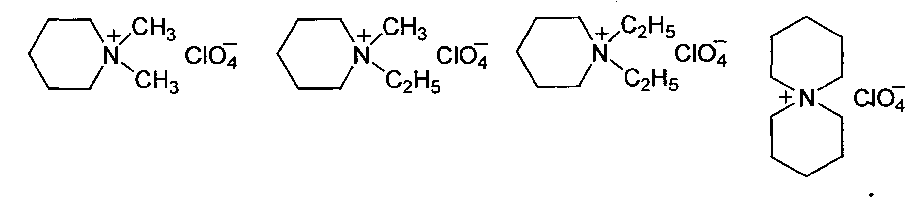
- Examples of such salts include quaternary ammonium salts such as (CH 3 ) 4 N + X - , (C 2 H 5 ) 4 N + X - , (n-C 4 H 9 ) 4 N + X - , and those represented by the following formulas: and phosphonium salts such as (CH 3 ) 4 P + X - , (C 2 H 5 ) 4 P + X - , (C 3 H 7 ) 4 P + X - , and (C 4 H 9 ) 4 P + X - .
- mixtures of these compounds may be suitably used.
- Redox ordinary-temperature melting salts may also be used as the substance exhibiting a reversible electrochemical oxidation-reduction characteristics.
- the term "redox ordinary-temperature melting salt” denotes a solvent-free salt comprising only ion pairs, in a melted state (liquid state) at ordinary temperature, more specifically denotes a salt comprising ion pairs which salt has a melting point of 20 °C or below and will be in a liquid state at a temperature exceeding 20 °C and are capable of inducing a reversible electrochemical oxidation-reduction reaction.
- One type of redox ordinary-temperature melting salts may be used alone, or two type or more thereof may be used in the form of a mixture.
- Examples of the redox ordinary-temperature melting salt include those represented by the following formulas: wherein R is an alkyl group having 2 to 20, preferably 2 to 10 carbon atoms and X - is a counter anion such as a halogen ion or SCN - ; wherein R1 and R2 are each independently an alkyl group having 1 to 10 carbon atoms, preferably methyl or ethyl or an aralkyl group having 7 to 20, preferably 7 to 13 carbon atoms, preferably benzyl and may be the same or different from each other and X - is a counter anion such as a halogen ion or SCN - ; wherein R 1 , R 2 , R 3 , and R 4 are each independently an alkyl group having one or more carbon atoms, preferably 1 to 6 carbon atoms, an aryl group having 6 to 12 carbon atoms such as phenyl, or a methoxymethyl group and may be the same or different from each other and
- the amount of the substance exhibiting reversible electrochemical oxidation-reduction characteristics is used as long as it is dissolved in any of the above-described solvents.
- the substance is used in an amount of 1 to 50 percent by mass and preferably 3 to 30 percent by mass based on the solvent.
- the supporting electrolyte to be added if necessary may be salts, acids, alkalis, ordinary-temperature melting salts which are generally used in the field of electrochemistry or electric batteries.
- the salts may be inorganic ion salts such as alkali metal salts and alkaline earth metal salts, quaternary ammonium salts, cyclic quaternary ammonium salts, and quaternary phosphonium salts. Particularly preferred are Li salts.
- the salts include Li, Na, and K salts having a counter anion selected from ClO 4 - , BF 4 - , CF 3 SO 3 - , (CF 3 SO 2 ) 2 N - , (C 2 F 5 SO 2 ) 2 N - , PF 6 - , AsF 6 - , CH 3 COO - , CH 3 (C 6 H 4 )SO 3 - , and (C 2 F 5 SO 2 ) 3 C - .
- a counter anion selected from ClO 4 - , BF 4 - , CF 3 SO 3 - , (CF 3 SO 2 ) 2 N - , (C 2 F 5 SO 2 ) 2 N - , PF 6 - , AsF 6 - , CH 3 COO - , CH 3 (C 6 H 4 )SO 3 - , and (C 2 F 5 SO 2 ) 3 C - .
- the salts may also be any of quaternary ammonium salts having a counter anion selected from ClO 4 - , BF 4 - , CF 3 SO 3 - , (CF 3 SO 2 ) 2 N - , (C 2 F 5 SO 2 ) 2 N - , PF 6 - , AsF 6 - , CH 3 COO - , CH 3 (C 6 H 4 )SO 3 - , and (C 2 F 5 SO 2 ) 3 C - , more specifically (CH 3 ) 4 N + BF 4 - , (C 2 H 5 ) 4 N + BF 4 - , (n-C 4 H 9 ) 4 N + BF 4 - , (C 2 H 5 ) 4 N + Br - , (C 2 H 5 ) 4 N + ClO 4 - , (n-C 4 H 9 ) 4 N + ClO 4 - , CH 3 (C 2 H 5 ) 3 N + BF 4 - , (CH
- More specific examples include (CH 3 ) 4 P + BF 4 - , (C 2 H 5 ) 4 P + BF 4 - , (C 3 H 7 ) 4 P + BF 4 - , and (C 4 H 9 ) 4 P + BF 4 - .
- the acids which, therefore, may be inorganic acids or organic acids.
- Specific examples of the acids are sulfuric acid, hydrochloric acid, phosphoric acids, sulfonic acids, and carboxylic acids.
- alkalis which, therefore, may be sodium hydroxide, potassium hydroxide, and lithium hydroxide.
- the ordinary-temperature melting salts used in the present invention are solvent-free salts comprising only ion pairs, in a melted state (liquid state) at ordinary temperature, more specifically salts comprising ion pairs which salts have a melting point of 20 °C or below and will be in a liquid state at a temperature exceeding 20 °C.
- One type of the ordinary-temperature melting salts may be used alone or alternatively two or more thereof may be used in the form of a mixture.
- Examples of the ordinary-temperature melting salt include those represented by the following formulas: wherein R is an alkyl group having 2 to 20, preferably 2 to 10 carbon atoms and X - is a counter anion selected from ClO 4 - , BF 4 - , (CF 3 SO 2 ) 2 N - , (C 2 F 5 SO 2 ) 2 N - , PF 6 - , AsF 6 - , CH 3 COO - , CH 3 (C 6 H 4 )SO 3 - , and (C 2 F 5 SO 2 ) 3 C - ; wherein R1 and R2 are each independently an alkyl group having 1 to 10 carbon atoms, preferably methyl or ethyl or an aralkyl group having 7 to 20, preferably 7 to 13 carbon atoms, preferably benzyl and may be the same or different from each other and X - is a counter anion selected from ClO 4 - , BF 4 - , (CF 3 SO 2 )
- the supporting electrolyte may be contained in an amount of usually 0.1 percent by mass or more, preferably 1 percent by mass or more, and more preferably 10 percent by mass or more and 70 percent by mass or less, preferably 60 percent by mass or less, and more preferably 50 percent by mass or less, in the electrolyte.
- polymeric solid electrolytes are particularly preferred because all the components of the photovoltaic device can be solid.
- particularly preferred polymeric solid electrolytes include those containing at least (c) a substance exhibiting reversible electrochemical oxidation-reduction characteristics (Component (c)) and if necessary further containing (b) a plasticizer (Component (b)), in (a) a polymeric matrix (Component (a)).
- optional components such as (d) any of the above-described supporting electrolyte or (e) an ultraviolet adsorbing agent or an amine compound may be contained in the polymeric solid electrolyte if necessary.
- the polymeric solid electrolyte is formed in a solid or gelled state by Component (b) or Components (b) and (c) and/or additional optional components retained in Component (a), i.e., the polymeric matrix.
- Component (a) i.e., polymeric matrix as long as they can be formed in a solid or gelled state by themselves or by addition of a plasticizer or a supporting electrolyte or the combination thereof.
- Polymeric compounds which have been generally used can be used in the present invention.
- polymeric compounds exhibiting characteristics of the polymeric matrix include polymeric compounds obtained by polymerizing or copolymerizing a monomer such as hexafluoropropylene, tetrafluoroethylene, trifluoroethylene, ethylene, propylene, acrylonitrile, vinylidene chloride, acrylic acid, methacrylic acid, methylacrylate, ethylacrylate, methylmethacrylate, styrene, and vinylidene fluoride. Any one of these polymeric compounds may be used alone or a mixture of any of these compounds may be used. In the present invention, polyvinylidene fluoride-based polymeric compounds are particularly preferably used.
- polyvinylidene fluoride-based polymeric compounds examples include homopolymers of vinylidene fluoride and copolymers of vinylidene fluoride and another polymerizable monomer, preferably a radical polymerizable monomer.
- another polymerizable monomer hereinafter referred to as "copolymerizable monomer" to be copolymerized with vinylidene fluoride include hexafluoropropylene, tetrafluoroethylene, trifluoroethylene, ethylene, propylene, acrylonitrile, vinylidene chloride, acrylic acid, methacrylic acid, methylacrylate, ethylacrylate, methylmethacrylate, and styrene.
- copolymerizable monomers may be used in an amount of 1 to 50 percent by mol, preferably 1 to 25 percent by mol, based on the total mass of the monomer.
- the copolymerizable monomer is preferably hexafluoropropylene.
- the polymeric solid electrolyte preferably contains a vinylidene fluoride-hexafluoropropylene copolymer obtained by copolymerizing 1 to 25 percent by mol of hexafluoropropylene with vinylidene fluoride, as the polymeric matrix.
- a mixture of two or more types of vinylidene fluoride-hexafluoropropylene copolymers with different copolymerization ratios may also be used.
- two or more of these copolymerizable monomers may be copolymerized with vinylidene fluoride.
- copolymers may be used which copolymers are obtained by copolymerizing vinylidene fluoride, hexafluoropropylene and tetrafluoroethylene; vinylidene fluoride, hexafluoropropylene and acrylic acid; vinylidene fluoride, tetrafluoroethylene and ethylene; or vinylidene fluoride, tetrafluoroethylene and propylene.
- the polymeric matrix may be a mixture of a polyvinyliden fluoride-based polymeric compound and one or more polymeric compounds selected from the group consisting of polyacrylic acid-based polymeric compounds, polyacrylate-based polymeric compounds, polymethacrylic acid-based polymeric compounds, polymethacrylate-based polymeric compounds, polyacrylonitrile-based polymeric compounds, and polyether-based polymeric compounds.
- the polymeric matrix may be a polyvinylidene fluoride-based polymeric compound may be a mixture of one or more copolymers obtained by copolymerizing a polyvinylidene fluoride-based polymeric compound with two or more monomers of the above-mentioned polymeric compounds.
- the blend ratio of the homopolymers or copolymers is usually 200 parts by mass or less, based on 100 parts by mass of the polyvinylidene fluoride-based polymeric compound.
- preferred polyvinylidene fluoride-based polymeric compounds are those having a weight-average molecular weight of generally from 10,000 to 2,000,000, preferably from 100,000 to 1,000,000.
- the plasticizer acts as a solvent of a substance exhibiting reversible electrochemical oxidation-reduction characteristics. Any type of plasticizers may be used as long as it can be generally used as an electrolyte solvent for electrochemical cells or electric cells. Specific examples include various solvents exemplified with respect to the liquid electrolyte.
- Preferred examples include propylene carbonate, ethylene carbonate, dimethylsulfoxide, dimethoxyethane, acetonitrile, ⁇ -butyrolactone, sulfolane, dioxolan, dimethylformamide, tetrahydrofuran, adiponitrile, methoxyacetonitrile, dimethylacetoamide, methylpyrrolidinone, trimethyl phosphate, and triethyl phosphate.
- ordinary-temperature melting salts may be used.
- ordinary-temperature melting salt denotes a solvent-free salt comprising only ion pairs, in a melted state (liquid state) at ordinary temperature, more specifically a salt comprising ion pairs which salt has a melting point of 20 °C or below and will be in a liquid state at a temperature exceeding 20 °C.
- Examples of the ordinary-temperature melting salt include those represented by the following formulas: wherein R is an alkyl group having 2 to 20, preferably 2 to 10 carbon atoms and X - is a halogen ion or SCN - ; wherein R1 and R2 are each independently an alkyl group having 1 to 10 carbon atoms, preferably methyl or ethyl or an aralkyl group having 7 to 20, preferably 7 to 13 carbon atoms, preferably benzyl and may be the same or different from each other and X - is a halogen ion or SCN - ; wherein R 1 , R 2 , R 3 , and R 4 are each independently an alkyl group having one or more carbon atoms, preferably 1 to 6 carbon atoms, an aryl group having 6 to 12 carbon atoms such as phenyl, or a methoxymethyl group and may be the same or different from each other and X - is a halogen ion or SCN
- plasticizers Any one of these plasticizers may be used alone or a mixture of two or more of these plasticizers may be used.
- the plasticizer may be contained in an amount of 20 percent by mass or more, preferably 50 percent by mass or more, and more preferably 70 percent by mass or more and 98 percent by mass or less, preferably 95 percent by mass or less, and more preferably 90 percent by mass or less, in the polymeric solid electrolyte.
- Component (c) i.e., substances exhibiting reversible electrochemical oxidation-reduction characteristics.
- Component (c) is a compound capable of inducing the above-described reversible electrochemical oxidation-reduction reaction and is generally referred to as a redox agent.
- Examples of the compound include ferrocene, p-benzoquinone, 7,7,8,8-tetracyanoquinodimethane, N,N,N',N'-tetramethyl-p-phenylenediamine, tetrathiafulvalene, anthracene, and p-toluylamine.
- the compound may also be LiI, NaI, KI, CsI, CaI 2 , iodine salts of quaternary imidazolium, iodine salts of tetraalkylammonium, Br 2 , and metal bromides such as LiBr, NaBr, KBr, CsBr or CaBr 2 .
- the compound may be tetraalkylammoniumbromide, bipyridiniumbromide, bromine salts, complex salts such as ferrocyanic acid-ferricyanate, sodium polysulfide, alkylthiol-alkyldisulfide, hydroquinone-quinone, or viologen.
- a reduced form Only either one of an oxidized form or a reduced form may be used as the redox agent.
- An oxidized form and a reduced form may be added in the form of a mixture mixed at a suitable molar ratio.
- Component (c) include salts having a counter anion (X - ) selected from halogen ions and SCN - .
- salts include quaternary ammonium salts such as (CH 3 ) 4 N + X - , (C 2 H 5 ) 4 N + X - , (n-C 4 H 9 ) 4 N + X - , and those represented by the following formulas: and phosphonium salts such as (CH 3 ) 4 P + X - , (C 2 H 5 ) 4 P + X - , (C 3 H 7 ) 4 P + X - , and (C 4 H 9 ) 4 P + X - .
- mixtures of these compounds may be suitably used.
- a redox ordinary-temperature melting salt may be used as Component (c).
- the term "redox ordinary-temperature melting salt” denotes a solvent-free salt comprising only ion pairs, in a melted state (liquid state) at ordinary temperature, more specifically denotes a salt comprising ion pairs which salt has a melting point of 20 °C or below and will be in a liquid state at a temperature exceeding 20 °C and are capable of inducing a reversible electrochemical oxidation-reduction reaction.
- Component (b) may or may not be used in combination.
- One type of the redox ordinary-temperature melting salts may be used alone or alternatively two or more types of the salts may be used in the form of a mixture.
- Examples of the redox ordinary-temperature melting salt include those represented by the following formulas: wherein R is an alkyl group having 2 to 20, preferably 2 to 10 carbon atoms and X - is a halogen ion or SCN - ; wherein R1 and R2 are each independently an alkyl group having 1 to 10 carbon atoms, preferably methyl or ethyl or an aralkyl group having 7 to 20, preferably 7 to 13 carbon atoms, preferably benzyl and may be the same or different from each other and X - is a halogen ion or SCN - ; wherein R 1 , R 2 , R 3 , and R 4 are each independently an alkyl group having one or more carbon atoms, preferably 1 to 6 carbon atoms, an aryl group having 6 to 12 carbon atoms such as phenyl, or a methoxymethyl group and may be the same or different from each other and X - is a halogen ion or
- Component (c) may be generally contained in an amount of usually 0.1 percent by mass or more, preferably 1 percent by mass or more, and more preferably 10 percent by mass or more and 70 percent by mass or less, preferably 60 percent by mass or less, more preferably 50 percent by mass or less, in the polymeric solid electrolyte.
- the mix ratio is desirously selected such that Component (c) is dissolved in Component (b) and does not precipitate after being formed into the polymeric solid electrolyte.
- the mix ratio by mass of Component (c)/Component (b) is in the range of preferably 0.01 to 0.5 and more preferably 0.03 to 0.3.
- the mass ratio of Component (a)/(Components (b) and (c)) is within the range of preferably 1/20 to 1/1, more preferably 1/10 to 1/2.
- the supporting electrolyte may be contained in an amount of usually 0.1 percent by mass or more, preferably 1 percent by mass or more, and more preferably 10 percent by mass or more and 70 percent by mass or less, preferably 60 percent by mass or less, and more preferably 50 percent by mass or less, in the polymeric solid electrolyte.
- the polymeric solid electrolyte may further contain other components.
- other components include ultraviolet adsorbing agents and amine compounds. No particular limitation is imposed on eligible ultraviolet adsorbing agent.
- Typical examples of the ultraviolet adsorbing agent include organic ultraviolet adsorbing agents such as compounds having a benzotriazole molecule structure or a benzophenone molecule structure.
- R 81 is hydrogen, halogen or an alkyl group having 1 to 10, preferably 1 to 6 carbon atoms.
- the halogen are fluorine, chlorine, bromine, and iodine.
- the alkyl group include methyl, ethyl, propyl, i-propyl, butyl, t-butyl and cyclohexyl groups.
- R 81 is usually substituted at the 4- or 5-position of the benzotriazole ring but the halogen and the alkyl group are usually located at the 4-position.
- R 82 is hydrogen or an alkyl group having 1 to 10, preferably 1 to 6 carbon atoms.
- alkyl group examples include methyl, ethyl, propyl, i-propyl, butyl, t-butyl, and cyclohexyl groups.
- R 83 is an alkylene or alkylidene group having 1 to 10, preferably 1 to 3 carbon atoms. Examples of the alkylene group include methylene, ethylene, trimethylene, and propylene groups. Examples of the alkylidene group include ethylidene and propylidene groups.
- the compounds represented by formula (1) include 3-(5-chloro-2H-benzotriazole-2-yl)-5-(1,1-dimethylethyl)-4-hydroxy-benzene propanoic acid, 3-(2H-benzotriazole-2-yl)-5-(1,1-dimethylethyl)-4-hydroxy-benzene ethanoic acid, 3-(2H-benzotriazole-2-yl)-4-hydroxybenzene ethanoic acid, 3-(5-methyl-2H-benzotriazole-2-yl)-5-(1-methylethyl)-4-hydroxybenzene propanoic acid, 2-(2'-hydroxy-5'-methylphenyl)benzotriazole, 2-[2'-hydroxy-3',5'-bis( ⁇ , ⁇ -dimethylbenzyl) phenyl] benzotriazole, 2-(2'-hydroxy-3', 5'-di-t-butylphenyl)benzotriazol,
- R 92 , R 93 , R 95 , R 96 , R 98 , and R 99 may be the same or different from each other and are each independently a hydroxyl group or an alkyl or alkoxy group having 1 to 10, preferably 1 to 6 carbon atoms.
- alkyl group include methyl, ethyl, propyl, i-propyl, butyl, t-butyl, and cyclohexyl groups.
- Specific examples of the alkoxy group are methoxy, ethoxy, propoxy, i-propoxy, and butoxy groups.
- R 91 , R 94 , and R 97 are each independently an alkylene or alkylidene group having 1 to 10, preferably 1 to 3 carbon atoms.
- alkylene group include methylene, ethylene, trimethylene, and propylene groups.
- alkylidene group include ethylidene and propylidene groups.
- p1, p2, p3, q1, q2, and q3 are each independently an integer of 0 to 3.
- Preferred examples of the compounds having a benzophenone molecule structure, represented by formulas (2) to (4) include 2-hydroxy-4-methoxybenzophenone-5-carboxylic acid, 2,2'-dihydroxy-4-methoxybenzophenone-5-carboxylic acid, 4-(2-hydroxybenzoyl)-3-hydroxybenzen propanoic acid, 2,4-dihydroxybenzophenone, 2-hydroxy-4-methoxybenzophenone, 2-hydroxy-4-methoxybenzophenone-5-sulfonic acid, 2-hydroxy-4-n-octoxybenzophenone, 2,2'-dihydroxy-4,4'-dimethoxybenzophenone, 2,2',4,4'-tetrahydroxybenzophenone, and 2-hydroxy-4-methoxy-2'-carboxybenzophenone.
- two or more of these ultraviolet adsorbing agents may be used in combination.
- the use of the ultraviolet adsorbing agent is optional. No particular limitation is imposed on the amount of the ultraviolet adsorbing agent to be used. However, if the agent is used, it may be contained in an amount of 0.1 percent by mass or more, preferably 1 percent by mass or more and 20 percent by mass or less and preferably 10 percent by mass or less, in the polymeric solid electrolyte.
- amine compounds which the polymeric solid electrolyte may contain No particular limitation is imposed on amine compounds which the polymeric solid electrolyte may contain.
- Various aliphatic and aromatic amines can be used.
- Typical examples of the amine compound include pyridine derivatives, bipyridine derivatives, and quinoline derivatives. It is expected that the open-circuit voltage is enhanced by addition of these amine compounds.
- Specific examples of these compounds include 4-t-butyl-pyridine, quinoline, and isoquinoline.
- the electrolyte may be produced as a redox electrolyte film, and the method for producing the same will be described next.
- the redox electrolyte film may be obtained by forming a mixture of Components (a) and (c) and optional components to be added if necessary into a film by a conventional method.
- a conventional method No particular limitation is imposed on the film forming method, which, therefore, may be any of extrusion, casting, spin-coating, and dip-coating methods.
- Extrusion may be conducted in a conventional manner wherein the mixture of the above-described components is formed into a film after being heat-melted.
- Casting is conducted by adjusting the viscosity of the mixture by adding thereto a suitable diluent, and coating and drying the diluted mixture with a conventional coater normally used for casting thereby forming the mixture into a film.
- a suitable diluent for casting thereby forming the mixture into a film.
- the coater include doctor coaters, blade coaters, rod coaters, knife coaters, reverse roll coaters, gravure coaters, spray coaters, and curtain coaters among which a suitable one is selected depending on the viscosity and film thickness.
- Spin coating is conducted by adjusting the viscosity of the mixture by adding a suitable diluent, and coating and drying the diluted mixture with a commercially available spin-coater thereby forming the mixture into a film.
- Dip coating is conducted by adjusting the viscosity of the mixture by adding a suitable diluent so as to obtain a solution of the mixture, dipping and lifting a suitable substrate therein, and drying the substrate thereby forming the mixture into a film.
- the semiconductor layer includes those of Bi 2 S 3 , CdS, CdSe, CdTe, CuInS 2 , CuInSe 2 , Fe 2 O 3 , GaP, GaAs, InP, Nb 2 O 5 , PbS, Si, SnO 2 , TiO 2 , WO 3 , ZnO, and ZnS, among which preferred are those of CdS, CdSe, CuInS 2 , CuInSe 2 , Fe 2 O 3 , GaAs, InP, Nb 2 O 5 , PbS, SnO 2 , TiO 2 , WO 3 , and ZnO. These materials may be used in combination. Particularly preferred are those of TiO 2 , ZnO, SnO 2 , and Nb 2 O 5 , while most preferred are those of TiO 2 and ZnO.
- the semiconductor used in the present invention may be monocrystalline or polycrystalline.
- the crystal system may be selected from those of anatase, rutile, or brookite type among which preferred are those of anatase type.
- the semiconductor layer may be formed by any suitable conventional method.
- the semiconductor layer may be obtained by coating a nanoparticle dispersant or sol solution, of the above-mentioned semiconductor on the substrate by any conventional method. No particular limitation is imposed on the coating method. Therefore, the coating may be conducted by a method wherein the semiconductor is obtained in the form of film by casting; spin-coating; dip-coating; bar-coating; and various printing methods such as screen-printing.
- the thickness of the semiconductor layer may be arbitrarily selected but is 0.5 ⁇ m or more and 50 ⁇ m or less, and preferably 1 ⁇ m or more and 20 ⁇ m or less.
- various dyes may be adsorbed to or contained in the layer.
- the dye to be used in the present invention can enhance the light-absorbing efficiency of the semiconductor layer.
- One or more of various metal complex dyes or organic dyes may be usually used.
- dyes having in their molecules a functional group such as carboxyl, hydroxyl, sulfonyl, phosphonyl, carboxylalkyl, hydroxyalkyl, sulfonylalkyl, and phosphonylalkyl groups are preferably used.
- Eligible metal complex dyes are a complex of ruthenium, osmium, iron, cobalt, or zinc; metal phthalocyanine; and chlorophyll.
- Examples of the metal complex dyes used in the present invention include those represented by the following formulas: wherein X is a univalent anion and two X may be independent of each other or cross-linked and are any of those represented by the following formulas: wherein X is a univalent anion and may be any of those represented by the following formulas: wherein Y is a univalent anion and may be any of halogen ions, SCN - , ClO 4 - , BF 4 - , CF 3 SO 3 - , (CF 3 SO 2 ) 2 N - , (C 2 F 5 SO 2 ) 2 N - , PF 6 - , AsF 6 - , CH 3 COO - , CH 3 (C 6 H 4 )SO 3 - , and (C 2 F 5 SO 2 ) 3 C - ; wherein Z is an atomic group having an unshared electron pair, and two Z may be independent of each other or cross-linked and any of those represented by the following
- Eligible organic dyes are cyanine-based dyes, hemicyanine-based dyes, merocyanine-based dyes, xanthene-based dyes, triphenylmethane-based dyes, and metal-free phthalocyanine-based dyes.
- dyes used in the present invention include those represented by the following formulas:
- the dye may be adsorbed to the semiconductor layer on a transparent electrically conductive substrate by coating a solution obtained by dissolving the dye in a solvent on the semiconductor layer by spray- or spin-coating and drying the solution.
- the substrate may be heated to a suitable temperature.
- the dye may be adsorbed to the semiconductor layer by dipping the layer into the solution. No particular limitation is imposed on the time for dipping as long as the dye is sufficiently adsorbed to the semiconductor layer.
- the substrate is dipped into the solution for preferably 1 to 30 hours, particularly preferably 5 to 20 hours. If necessary, the solvent or the substrate may be heated upon dipping.
- the concentration of the dye in the solution is preferably from 1 to 1,000 mM/L and more preferably from 10 to 500 mM/L.
- the solvent examples include alcohols such as methanol, ethanol, 1-propanol, 2-propanol, 1-butanol, 2-butanol, and t-butanol, nitrile-based solvents such as acetonitrile, propionitrile, methoxypropionitrile, and glutaronitrile, benzene, toluene, o-xylene, m-xylene, p-xylene, pentane, heptane, hexane, cyclohexane, heptane, ketones such as acetone, methyl ethyl ketone, diethyl ketone, and 2-butanone, diethylether, tetrahydrofuran, ethylene carbonate, propylene carbonate, nitromethane, dimethylformamide, dimethylsulfoxide, hex
- alcohols such as methanol, ethanol, 1-propanol, 2-propanol, 1-
- transparent electrically conductive substrate (hereinafter referred to as "transparent conductive substrate”) will be described next.
- the transparent conductive substrate is produced by laminating a transparent electrode layer over a transparent substrate.
- the material, thickness, size, and shape of the substrate can be properly selected depending on the purposes.
- the substrate may be selected from colored or colorless glasses, wire-reinforced glasses, glass blocks, and colored or colorless transparent resins.
- Specific examples are polyesters such as polyethylene terephthalate, polyamides, polysulfones, polyethersulfones, polyether ether ketones, polyphenylene sulfides, polycarbonates, polyimides, polymethyl methacrylates, polystyrenes, cellulose triacetates, and polymethyl pentenes.
- the term "transparent” used herein denotes a transmissivity of 10 to 100 percent.
- the substrates used herein are those having a smooth surface at ordinary temperature, which surface may be flat or curved or deformed with stress.
- the transparent electrode layer acting as an electrode may be a thin metal film of gold, silver, chromium, copper, or tungsten or an electrically conductive film made of a metal oxide.
- the metal oxide include those obtained by doping to tin oxide or zinc oxide trace amounts of components such as Indium Tin Oxide (ITO (In 2 O 3 :Sn)), Fluorine doped Tin Oxide (FTO (SnO 2 :F)), and Aluminum doped Zinc Oxide (AZO (ZnO:Al)).
- the film thickness is usually from 10 nm to 10 ⁇ m, preferably from 100 nm to 2 ⁇ m.
- the surface resistance (resistivity) is properly selected depending on the use of the substrate in the present invention, but is usually from 0.5 to 500 ⁇ /sq, preferably from 2 to 50 ⁇ /sq.
- the photovoltaic device of the present invention may be used as a photovoltaic device having a cross-section as shown in Fig. 1.
- the device has a substrate A composed of a transparent substrate and a semiconductor layer (titania and dye layers) formed thereon and a conductive counter electrode (substrate B) composed of a substrate and a conductive carbon layer formed thereon.
- substrate A composed of a transparent substrate and a semiconductor layer (titania and dye layers) formed thereon
- a conductive counter electrode substrate B
- the space defined between the substrates A and B is filled with an electrolytes, and the peripheral space of the device is sealed with a sealant.
- Lead wires (not shown) are connected to the electrically conductive portions of substrates A and B to take out electromotive force.
- the photovoltaic device of the present invention can be easily produced by a conventional method wherein the substrates A and B are sealed at their periphery and joined to each other with a predetermined space therebetween, and an electrolyte is put thereinto.
- the space between the substrates is generally 0.1 ⁇ m or larger and preferable 1 ⁇ m or larger and generally up to 1 mm and preferably 0.5 mm or smaller.
- a photovoltaic device with excellent durability can be provided at inexpensive material and production costs, using the counter electrode of the present invention.
- the resulting device is suitable for the use in solar batteries.
- thermosetting acrylic resin product name "Acrydic” manufactured by DAINIPPON INK AND CHEMICALS, INCORPORATED
- a melamine resin product name "Bansemin” manufactured by Harima Chemicals, Inc.
- graphite product name "USSP” manufactured by Nippon Graphite Industries, Ltd.
- the resulting conductive paste was bar-coated substantially over the entire surface of a 5 cm square glass substrate and heat-cured at a temperature of 160 °C for 0.5 hour. Thereafter, the cured paste was calcined under a nitrogen atmosphere at a temperature of 500 °C for 3 hours thereby obtaining a counter electrode having a conductive carbon layer.
- the thickness and surface resistance of the carbon layer was 50 ⁇ m and 50 ⁇ /sq, respectively.
- Ti-Nanoxide T manufactured by SOLARONIX was bar-coated over a 5 cm square SnO 2 :F glass (transparent conductive glass obtained by forming an SnO 2 :F film on a glass substrate) with a film resistivity of 30 ⁇ /sq and dried.
- SnO 2 :F glass transparent conductive glass obtained by forming an SnO 2 :F film on a glass substrate
- a film resistivity 30 ⁇ /sq and dried.
- the transparent conductive glass substrate was bar-coated, some pieces of Scotch-tape were attached to the 5 mm-width sides of the glass such that the thickness of the Ti-Nanoxide T was made uniform.
- the coated substrate was calcined at a temperature of 500 °C for 30 minutes.
- the substrate was dipped into a ruthenium dye represented by the formula below /ethanol solution (3.0 x 10 -4 mol/L) for 15 hours thereby forming a dye layer.
- a ruthenium dye represented by the formula below /ethanol solution (3.0 x 10 -4 mol/L) for 15 hours thereby forming a dye layer.
- the resulting glass substrate and the counter electrode obtained above were joined together.
- a propylene carbonate solution containing 0.3 mol/L lithium iodine and 0.03 mol/L iodine was infiltrated by capillary phenomenon to the contact portions of the substrate and the counter electrode, and the peripheries therebetween were sealed with an epoxy sealant.
- Lead wires were connected to the conductive layer portion of the transparent conductive substrate and the counter electrode.
- thermosetting acrylic resin product name "Acryl-G” manufactured by HONNY CHEMICAL CO., LTD.
- a melamine resin product name "NIKALAC SM551” manufactured by Sanwa Chemical Co., Ltd.
- ketjen black product name "ECP600JD” manufactured by MITSUBISHI CHEMICAL CORPORATION
- the resulting conductive paste was bar-coated substantially over the entire surface of a 5 cm square glass substrate and heat-cured at a temperature of 160 °C for 0.5 hour. Thereafter, the cured paste was calcined under a nitrogen atmosphere at a temperature of 500 °C for 3 hours thereby obtaining a counter electrode having a conductive carbon layer.
- the thickness and surface resistance of the carbon layer was 50 ⁇ m and 55 ⁇ /sq, respectively.
- Ti-Nanoxide T manufactured by SOLARONIX was bar-coated over a 5 cm square SnO 2 :F glass (transparent conductive glass obtained by forming an SnO 2 :F film on a glass substrate) with a film resistivity of 30 ⁇ /sq and dried.
- SnO 2 :F glass transparent conductive glass obtained by forming an SnO 2 :F film on a glass substrate
- a film resistivity 30 ⁇ /sq and dried.
- the transparent conductive glass substrate was bar-coated, some pieces of Scotch-tape were attached to the 5 mm-width sides of the glass such that the thickness of the Ti-Nanoxide T was made uniform.
- the coated substrate was calcined at a temperature of 500 °C for 30 minutes.
- the substrate was dipped into a ruthenium dye (product name "Ruthenium-535-bisTBA” manufactured by Solaronix) /ethanol solution (5.0 x 10 -4 mol/L) for 15 hours thereby forming a dye layer.
- ruthenium dye product name "Ruthenium-535-bisTBA” manufactured by Solaronix
- ethanol solution 5.0 x 10 -4 mol/L
- a 3-methoxypropionitrile solution containing 0.1 mol/L lithium iodine, 0.5 mol/L 1-propyl-2,3-dimethylimidazolium iodine, 0.5 mol/L 4-t-butylpyridine and 0.05 mol/L iodine was infiltrated by capillary phenomenon to the contact portions of the substrate and the counter electrode, and the peripheries therebetween were sealed with an epoxy sealant. Lead wires were connected to the conductive layer portion of the transparent conductive substrate and the counter electrode.
- thermosetting silicone resin product name "RZ-7705" manufactured by Nippon Unicar Company Limited
- ketjen black product name "ECP600JD” manufactured by MITSUBISHI CHEMICAL CORPORATION
- the resulting conductive paste was bar-coated substantially over the entire surface of a 5 cm square glass substrate and heat-cured at a temperature of 160 °C for 0.5 hour. Thereafter, the cured paste was calcined under a nitrogen atmosphere at a temperature of 500 °C for 3 hours thereby obtaining a counter electrode having a conductive carbon layer.
- the thickness and surface resistance of the carbon layer was 50 ⁇ m and 35 ⁇ /sq, respectively.
- Ti-Nanoxide T manufactured by SOLARONIX was bar-coated over a 5 cm square SnO 2 :F glass (transparent conductive glass obtained by forming an SnO 2 :F film on a glass substrate) with a film resistivity of 30 ⁇ /sq and dried.
- SnO 2 :F glass transparent conductive glass obtained by forming an SnO 2 :F film on a glass substrate
- a film resistivity 30 ⁇ /sq and dried.
- the transparent conductive glass substrate was bar-coated, some pieces of Scotch-tape were attached to the 5 mm-width sides of the glass such that the thickness of the Ti-Nanoxide T was made uniform.
- the coated substrate was calcined at a temperature of 500 °C for 30 minutes.
- the substrate was dipped into a ruthenium dye (product name "Ruthenium-620-1H-3TBA” manufactured by Solaronix) /ethanol solution (5.0 x 10 -4 mol/L) for 15 hours thereby forming a dye layer.
- a ruthenium dye product name "Ruthenium-620-1H-3TBA” manufactured by Solaronix
- ethanol solution 5.0 x 10 -4 mol/L
- a 3-methoxypropionitrile solution containing 0.1 mol/L lithium iodine, 0.5 mol/L 1-propyl-2,3-dimethylimidazolium iodine, 0.5 mol/L 4-t-butylpyridine and 0.05 mol/L iodine was infiltrated by capillary phenomenon to the contact portions of the substrate and the counter electrode, and the peripheries therebetween were sealed with an epoxy sealant. Lead wires were connected to the conductive layer portion of the transparent conductive substrate and the counter electrode.
Landscapes
- Engineering & Computer Science (AREA)
- Power Engineering (AREA)
- Microelectronics & Electronic Packaging (AREA)
- Chemical & Material Sciences (AREA)
- Chemical Kinetics & Catalysis (AREA)
- Electrochemistry (AREA)
- General Chemical & Material Sciences (AREA)
- Hybrid Cells (AREA)
- Photovoltaic Devices (AREA)
Abstract
A photovoltaic device is provided which device comprises at least a semiconductor layer formed on a transparent electrically conductive substrate, an electrolyte layer, and a counter electrode. The counter electrode is composed of a substrate and an electrically conductive carbon layer formed thereon. The photovoltaic device which is excellent in performance and can be easily produced is provided due to the use of the counter electrode. <IMAGE>
Description
The present invention relates to photovoltaic
devices suitable for photovoltaic power generation
applications such as solar batteries.
A photovoltaic device, so-called wet solar cell
such as a dye sensitized solar cell has on one side an
operative electrode arranged on a photosensitive layer
side and on the other side a counter electrode, an
electrolyte being disposed between these electrodes.
For such a photovoltaic device, the counter electrode
is an indispensable component to allow a redox reaction
to progress smoothly, but the use of a metallic counter
electrode has a drawback in that it is corroded by an
electrolyte. Alternatively, although a glass with a
transparent oxide conductive film, such as an SnO2:F
glass is generally used as a counter electrode, the use
of such a counter electrode is required to have a
precious metal exhibiting catalytic activity, such as
platinum deposited on one surface of the electrode so
as to bring the activation energy of the redox reaction
down. However, in order to deposit a precious metal
exhibiting catalytic activity such as platinum, vacuum
deposition or sputtering operation requiring
large-scale apparatuses must be conducted, and there
are a lot of problems in industrial sense to be solved,
such as those concerning production efficiency and
yield.
On the other hand, the use of porous activated
carbon for a counter electrode of a photovoltaic device
which is different from that mentioned above has been
proposed (H. Pettersson, T. Gruszecki, Solar Energy
Mater. Solar Cells, vol. 70, pp 203 (2001)). This
proposal had such restrictions in the production of the
device that a porous layer must be specially provided
between the operative electrode and the counter
electrode and be sealed as it absorbs an electrolyte
liquid. Alternatively, a method has been proposed in
which electrically conductive particles and carbon
material are mixed and pressurized to be formed into
a counter electrode. However, the device obtained by
this method had a low photoelectric conversion
efficiency (H. Lindstrom, A. Holmberg, E. Magnusson,
S. -E. Lindquist, L. Malmqvist, A. Hagfeldt, Nano Lett.,
vol. 1, pp 97 (2001)).
The present invention was made in view of the
foregoing situations and intends to provide a novel
counter electrode thereby being able to produce a
photovoltaic device which has excellent characteristic
performances and can be easily produced.
The present invention has been accomplished as a
result of extensive studies conducted to overcome the
above-described problems of the conventional products.
That is, the present invention relates to a
photovoltaic device having a counter electrode
comprising a substrate and an electrically conductive
carbon layer formed thereon.
Furthermore, the present invention also relates
to the photovoltaic device wherein the substrate is an
electrically conductive substrate.
The present invention will be described in more
detail below.
The counter electrode used in the present
invention is composed of a substrate and an
electrically conductive carbon layer (hereinafter
referred to as "conductive carbon layer") formed
thereon.
No particular limitation is imposed on the
substrate to be used in the invention. The material,
thickness, size, and shape of the substrate can be
properly selected depending on the purposes. The
substrate may or may not have conductivity. For
example, the substrate may be a metal such as gold and
platinum and also selected from colored or colorless
glasses, wire-reinforced glasses, glass blocks, and
colored or colorless transparent resins. Specific
examples of such resins include polyesters such as
polyethylene terephthalate, polyamides, polysulfones,
polyethersulfones, polyether ether ketones,
polyphenylene sulfides, polycarbonates, polyimides,
polymethyl methacrylates, polystyrenes, cellulose
triacetates, and polymethyl pentenes. The substrates
used herein are those having a smooth surface at
ordinary temperatures, which surface may be flat or
curved or deformable with stress. Alternatively, in
order to impart conductivity to the substrate, one of
the surfaces thereof may be coated with a thin metal
film of gold, silver, chromium, copper, or tungsten or
a conductive film made of a metal oxide. Preferred
examples of the metal oxide include those obtained by
doping to a metal oxide of tin or zinc trace amounts
of other metal elements, such as Indium Tin Oxide (ITO
(In2O3:Sn)), Fluorine doped Tin Oxide (FTO (SnO2:F)),
and Aluminum doped Zinc Oxide (AZO (ZnO:Al)).
The thickness of the conductive film is usually
from 10 nm to 10 µm and preferably from 100 nm to 2
µm. The surface resistance (resistivity) is usually
from 0.5 to 500 Ω/sq and preferably from 2 to 50 Ω
/sq. The conductive film may be formed on a substrate
in any conventional manner such as vacuum deposition,
ion plating, CVD, electron beam vacuum deposition, and
sputtering.
The conductive carbon layer may be arranged on the
above-described substrate or the conductive film
formed thereon. No particular limitation is imposed
on the form of the conductive carbon layer to be arranged.
Therefore, the conductive carbon layer may be arranged
in the form of mesh or stripe on the entire or a part
of the substrate surface.
In the case of arranging the conductive carbon
layer on a part of the substrate, the substrate is
preferably that having conductivity. In this case, no
particular limitation is imposed on the coverage rate
(area ratio) of the conductive carbon layer against the
substrate. However, the conductive carbon layer
covers preferably 50 percent or more, more preferably
80 percent or more, and further more preferably 90
percent or more of the substrate with the objective of
sufficient performances of the conductive carbon layer.
No particular limitation is imposed on the mesh or
stripe form. Therefore, the mesh or stripe may be
formed by straight or curved lines. No particular
limitation is imposed on the width of lines or the size
of mesh, which, therefore, may be selected depending
on the type of conductive material . The lines have
a width of preferably from 1 µm to 10 mm and
particularly preferably from 2 µm to 5 mm and are spaced
at intervals of usually from 1 µm to 10 cm and
preferably from 2 µm to 5 cm.
The thickness of the conductive carbon layer is
usually from 1 µm to 1 mm and preferably from 2 µm to
0.5 mm.
The conductivity (electric conductivity) of the
conductive carbon layer is usually 200 Ω/sq or lower
and preferably 20 Ω/sq or lower.
No particular limitation is imposed on conductive
carbon materials forming the conductive carbon layer
as long as they have conductivity suitable for the
present invention. Examples of the materials include
black lead or graphite, glassy carbon, acetylene black,
Ketjen black, carbon fiber, activated carbon,
petroleum coke, fullerenes such as C60 and C70, and
single or multi layered carbon nanotube. Preferred are
black lead and carbon fiber. No particular limitation
is imposed on the shape of conductive carbon materials
as long as they can be eventually formed into a carbon
layer. Therefore, the material may be in the form of
powder, discontinuous or continuous fiber, or woven or
non-woven cloth.
In the case of using a powder material, it is
preferably that having an adequate specific surface
area. The specific surface area is preferably from 100
to 2,000 m2/g and more preferably from 300 to 1,000 m2/g.
The average particle size is from 5 to 1,000 nm and
preferably from 8 to 200 nm.
The conductive carbon layer may be composed of
only any of the above-described conductive carbon
materials but may contain another optional component
as long as the object of the present invention can be
achieved.
For example, a binder is preferably used for
purpose of enhancing the conductivity through a raw
material such as carbon powder or discontinuous or
continuous fiber. No particular limitation is imposed
on such a binder as long as it is inactive to and not
electrolyzed in an electrolyte after being cured.
Examples of such a binder include polymeric solid
electrolytes, epoxy resins, acrylic resins, melamine
resins, silicone resins, polytetrafluoro ethylene,
polystyrol, carboxymethyl cellulose, polyvinylidene
fluoride, derivatives of these compounds, and mixtures
of any of these compounds. When any of these binders
is used, the mix ratio of conductive carbon
material/binder (mass ratio) is usually from 10/90 to
90/10 and preferably from 20/80 to 80/20.
Examples of other optional components include
metal fine particles having properties that they are
not corroded with an electrolyte and conductive oxide
semiconductors such as ITO, FTO, and AZO.
No particular limitation is imposed on the method
of forming the conductive carbon layer. Therefore, any
conventional method may be used. For example, in the
case of using a binder, the conductive carbon layer is
formed by a method wherein any of the above-described
conductive carbon materials and a binder are mixed and
formed into paste and then printed on a surface of a
substrate by a special printing technique such as
screen printing, surface printing, gravure printing,
intaglio printing, flexographic printing, or
letterpress printing or a method wherein any of the
above-described conductive carbon materials and a
binder are mixed and formed into paste and then filled
into grooves having been formed on a substrate
beforehand and excess paste is removed with a spatula.
After the paste is coated on a surface of a substrate,
it may be heated so as to improve the conductivity or
adhesivity. Heating may be conducted with an oven, a
muffle furnace, or an electric furnace or utilizing
infrared heating. Although the heating temperature is
varied depending on the type of paste or substrate to
be used, it is preferably from 50°C to 700°C, more
preferably from 100°C to 600°C, and further more
preferably from 200°C to 500°C. If necessary, heating
may be conducted under a nitrogen atmosphere.
Alternatively, any of the conductive carbon materials
shaped into a thin film, a woven or non-woven cloth,
a felt or a paper-like sheet may be laminated on a
substrate.
The photovoltaic device of the present invention
is characterized by using the counter electrode thus
obtained and essentially comprises a transparent
conductive substrate, a photovoltaic layer
(semiconductor layer) formed thereon, and the counter
electrode. Although the photovoltaic layer may be in
direct contact with the counter electrode, an
electrolyte layer is usually arranged therebetween.
Examples of the photovoltaic device include those
having a structure as shown in Fig. 1.
No particular limitation is imposed on the
electrolyte. Therefore, the electrolyte may be of
liquid or solid type and is preferably that exhibiting
reversible electrochemical oxidation-reduction
characteristics.
The electrolyte is that having an ion conductivity
of generally 1 x 10⁻⁷ S/cm or higher, preferably 1 x
10-6 S/cm or higher, and more preferably 1 x 10⁻⁵ S/cm
or higher, at room temperatures. The ion conductivity
can be sought by a conventional method such as complex
impedance method.
The electrolyte used in the present invention are
those whose oxidized form has a diffusion coefficient
of 1 x 10⁻⁹ cm2/s or higher, preferably 1 x 10⁻⁸ cm2/s
or higher, and more preferably 1 x 10⁻⁷ cm2/s or higher.
The diffusion coefficient is one of the indices
indicating ion conductivity and can be sought by any
of conventional techniques such as a constant potential
current characteristics measurement and a cyclic
voltammogram measurement.
No particular limitation is imposed on the
thickness of the electrolyte layer. The thickness is
preferably 1 µm or more, more preferably 10 µm or more
and preferably 3 mm or less and more preferably 1 mm
or less.
No particular limitation is imposed on the liquid
type electrolyte. The electrolyte is usually composed
of a solvent, a substance exhibiting reversible
electrochemical oxidation-reduction characteristics
and dissoluble in the solvent, and if necessary a
supporting electrolyte, as essential components.
The solvent may be any solvent as long as it is
generally used for electrochemical cells or electric
batteries. Specific examples of the solvent include
acetic anhydride, methanol, ethanol, tetrahydrofuran,
propylene carbonate, nitromethane, acetonitrile,
dimethylformamide, dimethylsulfoxide,
hexamethylphosphoamide, ethylene carbonate,
dimethoxyethane, γ-butyrolactone, γ-valerolactone,
sulfolane, propionnitrile, glutaronitrile,
adiponitrile, methoxyacetonitrile,
methoxypropionitrile, dimethylacetoamide,
methylpyrrolidinone, dioxolane, trimethyl phosphate,
triethyl phosphate, tripropyl phosphate,
ethyldimethyl phosphate, tributyl phosphate,
tripentyl phosphate, trihexyl phosphate, triheptyl
phosphate, trioctyl phosphate, trinonyl phosphate,
tridecyl phosphate, tris(trifluoromethyl)phosphate,
tris(pentafluoroethyl)phosphate,
triphenylpolyethylene glycol phosphate, and
polyethylene glycol. Particularly preferred examples
include propylene carbonate, ethylene carbonate,
dimethylsulfoxide, dimethoxyethane, acetonitrile, γ-butyrolactone,
sulfolane, dioxolane,
dimethylformamide, tetrahydrofuran, adiponitrile,
methoxyacetonitrile, methoxypropionitrile,
dimethylacetoamide, methylpyrrolidinone, trimethyl
phosphate, and triethyl phosphate. One of these
solvents may be used alone or two or more of the solvents
may be used in the form of a mixture.
The substance exhibiting reversible
electrochemical oxidation-reduction characteristics
is generally referred to as a redox agent. No
particular limitation is imposed on the type of the
redox agent. Examples of the substance include
ferrocene, p-benzoquinone,
7,7,8,8-tetracyanoquinodimethane,
N,N,N',N'-tetramethyl-p-phenylenediamine,
tetrathiafulvalene, thianthracene, and p-toluylamine.
The substance may also be LiI, NaI, KI, CsI, CaI2, iodine
salts of quaternary imidazolium, iodine salts of
tetraalkylammonium, Br2, and metal bromides such as
LiBr, NaBr, KBr, CsBr or CaBr2. Further, the substance
may be tetraalkylammoniumbromide, bipyridiniumbromide,
bromine salts, complex salts such as ferrocyanic
acid-ferricyanate, sodium polysulfide,
alkylthiol-alkyldisulfide, hydroquinone-quinone, or a
viologen dye.
Only either one of an oxidized form or a reduced
form may be used as the redox agent. An oxidized form
and a reduced form may be added in the form of a mixture
mixed at a suitable molar ratio. Alternatively, an
oxidation-reduction pair may be added such that the
electrolyte exhibits electrochemical response
properties. Examples of materials exhibiting such
properties include metallocenium salts such as
ferrocenium having a counter anion selected from
halogen ions, SCN-, ClO4 -, BF4 -, CF3SO3 -, (CF3SO2)2N-,
(C2F5SO2)2N-, PF6 -, AsF6 -, CH3COO-, CH3(C6H4)SO3 -, and
(C2F5SO2)3C- and halogens such as iodine, bromine, and
chlorine.
Examples of substances exhibiting a reversible
electrochemical oxidation-reduction characteristics
include salts having a counter anion (X-) selected from
halogen ions and SCN-. Examples of such salts include
quaternary ammonium salts such as (CH3)4N+X-, (C2H5)4N+X-,
(n-C4H9)4N+X-, and those represented by the following
formulas:

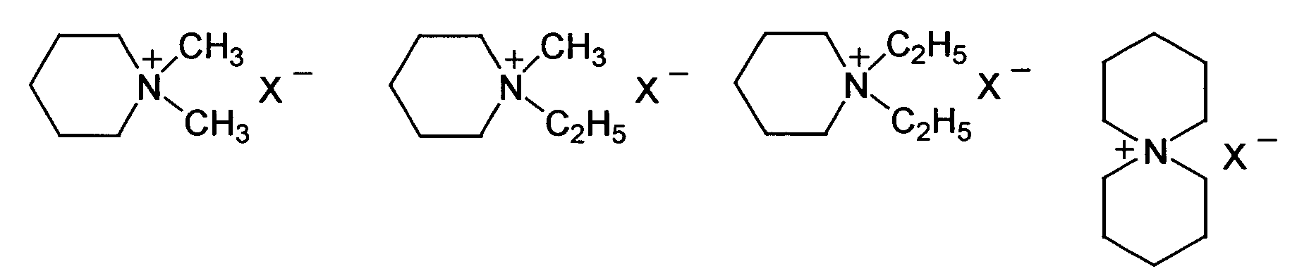 and phosphonium salts such as (CH3)4P+X-, (C2H5)4P+X-,
(C3H7)4P+X-, and (C4H9)4P+X-.
and phosphonium salts such as (CH3)4P+X-, (C2H5)4P+X-,
(C3H7)4P+X-, and (C4H9)4P+X-.
Needless to mention, mixtures of these compounds
may be suitably used.
Redox ordinary-temperature melting salts may also
be used as the substance exhibiting a reversible
electrochemical oxidation-reduction characteristics.
The term "redox ordinary-temperature melting salt"
denotes a solvent-free salt comprising only ion pairs,
in a melted state (liquid state) at ordinary
temperature, more specifically denotes a salt
comprising ion pairs which salt has a melting point of
20 °C or below and will be in a liquid state at a
temperature exceeding 20 °C and are capable of inducing
a reversible electrochemical oxidation-reduction
reaction.
One type of redox ordinary-temperature melting
salts may be used alone, or two type or more thereof
may be used in the form of a mixture.
Examples of the redox ordinary-temperature
melting salt include those represented by the following
formulas:
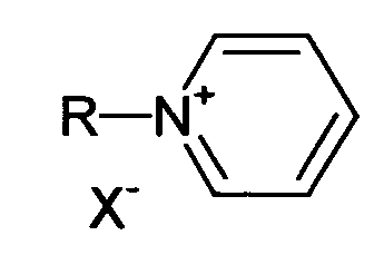 wherein R is an alkyl group having 2 to 20, preferably
2 to 10 carbon atoms and X- is a counter anion such as
a halogen ion or SCN-;
wherein R is an alkyl group having 2 to 20, preferably
2 to 10 carbon atoms and X- is a counter anion such as
a halogen ion or SCN-;
 wherein R1 and R2 are each independently an alkyl group
having 1 to 10 carbon atoms, preferably methyl or ethyl
or an aralkyl group having 7 to 20, preferably 7 to 13
carbon atoms, preferably benzyl and may be the same or
different from each other and X- is a counter anion such
as a halogen ion or SCN-;
wherein R1 and R2 are each independently an alkyl group
having 1 to 10 carbon atoms, preferably methyl or ethyl
or an aralkyl group having 7 to 20, preferably 7 to 13
carbon atoms, preferably benzyl and may be the same or
different from each other and X- is a counter anion such
as a halogen ion or SCN-;
 wherein R1, R2, R3, and R4 are each independently an alkyl
group having one or more carbon atoms, preferably 1 to
6 carbon atoms, an aryl group having 6 to 12 carbon atoms
such as phenyl, or a methoxymethyl group and may be the
same or different from each other and X- is a counter
anion such as a halogen ion or SCN-.
wherein R1, R2, R3, and R4 are each independently an alkyl
group having one or more carbon atoms, preferably 1 to
6 carbon atoms, an aryl group having 6 to 12 carbon atoms
such as phenyl, or a methoxymethyl group and may be the
same or different from each other and X- is a counter
anion such as a halogen ion or SCN-.
No particular limitation is imposed on the amount
of the substance exhibiting reversible electrochemical
oxidation-reduction characteristics to be used as long
as it is dissolved in any of the above-described
solvents. However, the substance is used in an amount
of 1 to 50 percent by mass and preferably 3 to 30 percent
by mass based on the solvent.
The supporting electrolyte to be added if
necessary may be salts, acids, alkalis,
ordinary-temperature melting salts which are generally
used in the field of electrochemistry or electric
batteries.
No particular limitation is imposed on the salts.
For example, the salts may be inorganic ion salts such
as alkali metal salts and alkaline earth metal salts,
quaternary ammonium salts, cyclic quaternary ammonium
salts, and quaternary phosphonium salts.
Particularly preferred are Li salts.
Specific examples of the salts include Li, Na, and
K salts having a counter anion selected from ClO4 -, BF4 -,
CF3SO3 -, (CF3SO2)2N-, (C2F5SO2)2N-, PF6 -, AsF6 -, CH3COO-,
CH3(C6H4)SO3 -, and (C2F5SO2)3C-.
The salts may also be any of quaternary ammonium
salts having a counter anion selected from ClO4 -, BF4 -,
CF3SO3 -, (CF3SO2)2N-, (C2F5SO2)2N-, PF6 -, AsF6 -, CH3COO-,
CH3(C6H4)SO3 -, and (C2F5SO2)3C-, more specifically
(CH3)4N+BF4 -, (C2H5)4N+BF4 -, (n-C4H9)4N+BF4 -, (C2H5)4N+Br-,
(C2H5)4N+ClO4 -, (n-C4H9)4N+ClO4 -, CH3(C2H5)3N+BF4 -,
(CH3)2(C2H5)2N+BF4 -, (CH3)4N+SO3CF3 -, (C2H5)4N+SO3CF3 -,
(n-C4H9)4N+SO3CF3 -, and those represented by the
following formulas:

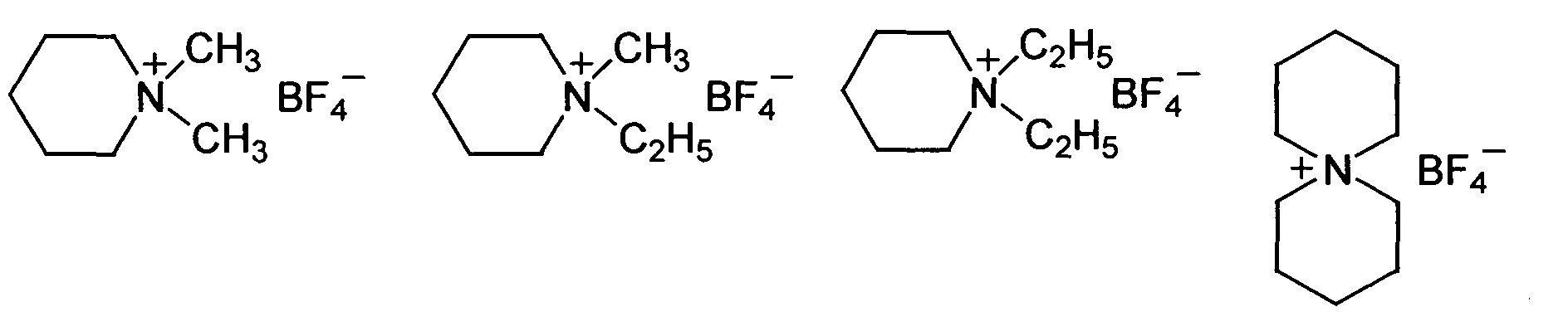

 Furthermore, the salts may be any of phosphonium salts
having a counter anion selected from ClO4 -, BF4 -, CF3SO3 -,
(CF3SO2)2N-, (C2F5SO2)2N-, PF6 -, AsF6 -, CH3COO-,
CH3(C6H4)SO3 -, and (C2F5SO2)3C-. More specific examples
include (CH3)4P+BF4 -, (C2H5)4P+BF4 -, (C3H7)4P+BF4 -, and
(C4H9)4P+BF4 -.
Furthermore, the salts may be any of phosphonium salts
having a counter anion selected from ClO4 -, BF4 -, CF3SO3 -,
(CF3SO2)2N-, (C2F5SO2)2N-, PF6 -, AsF6 -, CH3COO-,
CH3(C6H4)SO3 -, and (C2F5SO2)3C-. More specific examples
include (CH3)4P+BF4 -, (C2H5)4P+BF4 -, (C3H7)4P+BF4 -, and
(C4H9)4P+BF4 -.
Mixtures of these compounds may be suitably used
in the present invention.
No particular limitation is imposed on the acids,
which, therefore, may be inorganic acids or organic
acids. Specific examples of the acids are sulfuric
acid, hydrochloric acid, phosphoric acids, sulfonic
acids, and carboxylic acids.
No particular limitation is imposed on the alkalis
which, therefore, may be sodium hydroxide, potassium
hydroxide, and lithium hydroxide.
No particular limitation is imposed on the
ordinary-temperature melting salts. The
ordinary-temperature melting salts used in the present
invention are solvent-free salts comprising only ion
pairs, in a melted state (liquid state) at ordinary
temperature, more specifically salts comprising ion
pairs which salts have a melting point of 20 °C or below
and will be in a liquid state at a temperature exceeding
20 °C.
One type of the ordinary-temperature melting
salts may be used alone or alternatively two or more
thereof may be used in the form of a mixture.
Examples of the ordinary-temperature melting salt
include those represented by the following formulas:
 wherein R is an alkyl group having 2 to 20, preferably
2 to 10 carbon atoms and X- is a counter anion selected
from ClO4 -, BF4 -, (CF3SO2)2N-, (C2F5SO2)2N-, PF6 -, AsF6 -,
CH3COO-, CH3(C6H4)SO3 -, and (C2F5SO2)3C-;
wherein R is an alkyl group having 2 to 20, preferably
2 to 10 carbon atoms and X- is a counter anion selected
from ClO4 -, BF4 -, (CF3SO2)2N-, (C2F5SO2)2N-, PF6 -, AsF6 -,
CH3COO-, CH3(C6H4)SO3 -, and (C2F5SO2)3C-;
 wherein R1 and R2 are each independently an alkyl group
having 1 to 10 carbon atoms, preferably methyl or ethyl
or an aralkyl group having 7 to 20, preferably 7 to 13
carbon atoms, preferably benzyl and may be the same or
different from each other and X- is a counter anion
selected from ClO4 -, BF4 -, (CF3SO2)2N-, (C2F5SO2)2N-, PF6 -,
AsF6 -, CH3COO-, CH3(C6H4)SO3 -, and (C2F5SO2)3C-; and
wherein R1 and R2 are each independently an alkyl group
having 1 to 10 carbon atoms, preferably methyl or ethyl
or an aralkyl group having 7 to 20, preferably 7 to 13
carbon atoms, preferably benzyl and may be the same or
different from each other and X- is a counter anion
selected from ClO4 -, BF4 -, (CF3SO2)2N-, (C2F5SO2)2N-, PF6 -,
AsF6 -, CH3COO-, CH3(C6H4)SO3 -, and (C2F5SO2)3C-; and
 wherein R1, R2, R3, and R4 are each independently an alkyl
group having one or more carbon atoms, preferably 1 to
6 carbon atoms, an aryl group having 6 to 12 carbon atoms
such as phenyl, or a methoxymethyl group and may be the
same or different from each other and X- is a counter
anion selected from ClO4 -, BF4 -, (CF3SO2)2N-, (C2F5SO2)2N-,
PF6 -, AsF6 -, CH3COO-, CH3(C6H4)SO3 -, and (C2F5SO2)3C-.
wherein R1, R2, R3, and R4 are each independently an alkyl
group having one or more carbon atoms, preferably 1 to
6 carbon atoms, an aryl group having 6 to 12 carbon atoms
such as phenyl, or a methoxymethyl group and may be the
same or different from each other and X- is a counter
anion selected from ClO4 -, BF4 -, (CF3SO2)2N-, (C2F5SO2)2N-,
PF6 -, AsF6 -, CH3COO-, CH3(C6H4)SO3 -, and (C2F5SO2)3C-.
No particular limitation is imposed on the amount
of the supporting electrolyte to be used. The
supporting electrolyte may be contained in an amount
of usually 0.1 percent by mass or more, preferably 1
percent by mass or more, and more preferably 10 percent
by mass or more and 70 percent by mass or less,
preferably 60 percent by mass or less, and more
preferably 50 percent by mass or less, in the
electrolyte.
Although the above-described liquid electrolytes
may be used as the electrolyte used in the present
invention, polymeric solid electrolytes are
particularly preferred because all the components of
the photovoltaic device can be solid. Examples of
particularly preferred polymeric solid electrolytes
include those containing at least (c) a substance
exhibiting reversible electrochemical
oxidation-reduction characteristics (Component (c))
and if necessary further containing (b) a plasticizer
(Component (b)), in (a) a polymeric matrix (Component
(a)). In addition to these components, optional
components such as (d) any of the above-described
supporting electrolyte or (e) an ultraviolet adsorbing
agent or an amine compound may be contained in the
polymeric solid electrolyte if necessary. The
polymeric solid electrolyte is formed in a solid or
gelled state by Component (b) or Components (b) and (c)
and/or additional optional components retained in
Component (a), i.e., the polymeric matrix.
No particular limitation is imposed on materials
usable for Component (a), i.e., polymeric matrix as
long as they can be formed in a solid or gelled state
by themselves or by addition of a plasticizer or a
supporting electrolyte or the combination thereof.
Polymeric compounds which have been generally used can
be used in the present invention.
Examples of polymeric compounds exhibiting
characteristics of the polymeric matrix include
polymeric compounds obtained by polymerizing or
copolymerizing a monomer such as hexafluoropropylene,
tetrafluoroethylene, trifluoroethylene, ethylene,
propylene, acrylonitrile, vinylidene chloride,
acrylic acid, methacrylic acid, methylacrylate,
ethylacrylate, methylmethacrylate, styrene, and
vinylidene fluoride. Any one of these polymeric
compounds may be used alone or a mixture of any of these
compounds may be used. In the present invention,
polyvinylidene fluoride-based polymeric compounds are
particularly preferably used.
Examples of the polyvinylidene fluoride-based
polymeric compounds include homopolymers of vinylidene
fluoride and copolymers of vinylidene fluoride and
another polymerizable monomer, preferably a radical
polymerizable monomer. Examples of the another
polymerizable monomer (hereinafter referred to as
"copolymerizable monomer") to be copolymerized with
vinylidene fluoride include hexafluoropropylene,
tetrafluoroethylene, trifluoroethylene, ethylene,
propylene, acrylonitrile, vinylidene chloride,
acrylic acid, methacrylic acid, methylacrylate,
ethylacrylate, methylmethacrylate, and styrene.
These copolymerizable monomers may be used in an
amount of 1 to 50 percent by mol, preferably 1 to 25
percent by mol, based on the total mass of the monomer.
The copolymerizable monomer is preferably
hexafluoropropylene. The polymeric solid electrolyte
preferably contains a vinylidene
fluoride-hexafluoropropylene copolymer obtained by
copolymerizing 1 to 25 percent by mol of
hexafluoropropylene with vinylidene fluoride, as the
polymeric matrix. A mixture of two or more types of
vinylidene fluoride-hexafluoropropylene copolymers
with different copolymerization ratios may also be
used.
Alternatively, two or more of these
copolymerizable monomers may be copolymerized with
vinylidene fluoride. For example, copolymers may be
used which copolymers are obtained by copolymerizing
vinylidene fluoride, hexafluoropropylene and
tetrafluoroethylene; vinylidene fluoride,
hexafluoropropylene and acrylic acid; vinylidene
fluoride, tetrafluoroethylene and ethylene; or
vinylidene fluoride, tetrafluoroethylene and
propylene.
Furthermore, in the present invention, the
polymeric matrix may be a mixture of a polyvinyliden
fluoride-based polymeric compound and one or more
polymeric compounds selected from the group consisting
of polyacrylic acid-based polymeric compounds,
polyacrylate-based polymeric compounds,
polymethacrylic acid-based polymeric compounds,
polymethacrylate-based polymeric compounds,
polyacrylonitrile-based polymeric compounds, and
polyether-based polymeric compounds. Alternatively,
the polymeric matrix may be a polyvinylidene
fluoride-based polymeric compound may be a mixture of
one or more copolymers obtained by copolymerizing a
polyvinylidene fluoride-based polymeric compound with
two or more monomers of the above-mentioned polymeric
compounds. The blend ratio of the homopolymers or
copolymers is usually 200 parts by mass or less, based
on 100 parts by mass of the polyvinylidene
fluoride-based polymeric compound.
In the present invention, preferred
polyvinylidene fluoride-based polymeric compounds are
those having a weight-average molecular weight of
generally from 10,000 to 2,000,000, preferably from
100,000 to 1,000,000.
The plasticizer (Component (b)) acts as a solvent
of a substance exhibiting reversible electrochemical
oxidation-reduction characteristics. Any type of
plasticizers may be used as long as it can be generally
used as an electrolyte solvent for electrochemical
cells or electric cells. Specific examples include
various solvents exemplified with respect to the liquid
electrolyte. Preferred examples include propylene
carbonate, ethylene carbonate, dimethylsulfoxide,
dimethoxyethane, acetonitrile, γ-butyrolactone,
sulfolane, dioxolan, dimethylformamide,
tetrahydrofuran, adiponitrile, methoxyacetonitrile,
dimethylacetoamide, methylpyrrolidinone, trimethyl
phosphate, and triethyl phosphate. Alternatively,
ordinary-temperature melting salts may be used. The
term "ordinary-temperature melting salt" used herein
denotes a solvent-free salt comprising only ion pairs,
in a melted state (liquid state) at ordinary
temperature, more specifically a salt comprising ion
pairs which salt has a melting point of 20 °C or below
and will be in a liquid state at a temperature exceeding
20 °C.
Examples of the ordinary-temperature melting salt
include those represented by the following formulas:
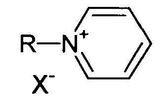 wherein R is an alkyl group having 2 to 20, preferably
2 to 10 carbon atoms and X- is a halogen ion or SCN-;
wherein R is an alkyl group having 2 to 20, preferably
2 to 10 carbon atoms and X- is a halogen ion or SCN-;
 wherein R1 and R2 are each independently an alkyl group
having 1 to 10 carbon atoms, preferably methyl or ethyl
or an aralkyl group having 7 to 20, preferably 7 to 13
carbon atoms, preferably benzyl and may be the same or
different from each other and X- is a halogen ion or
SCN-;
wherein R1 and R2 are each independently an alkyl group
having 1 to 10 carbon atoms, preferably methyl or ethyl
or an aralkyl group having 7 to 20, preferably 7 to 13
carbon atoms, preferably benzyl and may be the same or
different from each other and X- is a halogen ion or
SCN-;
 wherein R1, R2, R3, and R4 are each independently an alkyl
group having one or more carbon atoms, preferably 1 to
6 carbon atoms, an aryl group having 6 to 12 carbon atoms
such as phenyl, or a methoxymethyl group and may be the
same or different from each other and X- is a halogen
ion or SCN-.
wherein R1, R2, R3, and R4 are each independently an alkyl
group having one or more carbon atoms, preferably 1 to
6 carbon atoms, an aryl group having 6 to 12 carbon atoms
such as phenyl, or a methoxymethyl group and may be the
same or different from each other and X- is a halogen
ion or SCN-.
Any one of these plasticizers may be used alone
or a mixture of two or more of these plasticizers may
be used.
No particular limitation is imposed on the amount
of the plasticizer to be used. The plasticizer may be
contained in an amount of 20 percent by mass or more,
preferably 50 percent by mass or more, and more
preferably 70 percent by mass or more and 98 percent
by mass or less, preferably 95 percent by mass or less,
and more preferably 90 percent by mass or less, in the
polymeric solid electrolyte.
Next described will be Component (c), i.e.,
substances exhibiting reversible electrochemical
oxidation-reduction characteristics.
Component (c) is a compound capable of inducing
the above-described reversible electrochemical
oxidation-reduction reaction and is generally referred
to as a redox agent.
No particular limitation is imposed on the type
of such a compound. Examples of the compound include
ferrocene, p-benzoquinone,
7,7,8,8-tetracyanoquinodimethane,
N,N,N',N'-tetramethyl-p-phenylenediamine,
tetrathiafulvalene, anthracene, and p-toluylamine.
The compound may also be LiI, NaI, KI, CsI, CaI2, iodine
salts of quaternary imidazolium, iodine salts of
tetraalkylammonium, Br2, and metal bromides such as
LiBr, NaBr, KBr, CsBr or CaBr2.
Further, the compound may be
tetraalkylammoniumbromide, bipyridiniumbromide,
bromine salts, complex salts such as ferrocyanic
acid-ferricyanate, sodium polysulfide,
alkylthiol-alkyldisulfide, hydroquinone-quinone, or
viologen. Only either one of an oxidized form or a
reduced form may be used as the redox agent. An
oxidized form and a reduced form may be added in the
form of a mixture mixed at a suitable molar ratio.
Particular examples of Component (c) include
salts having a counter anion (X-) selected from halogen
ions and SCN-. Examples of such salts include
quaternary ammonium salts such as (CH3)4N+X-, (C2H5)4N+X-,
(n-C4H9)4N+X-, and those represented by the following
formulas:

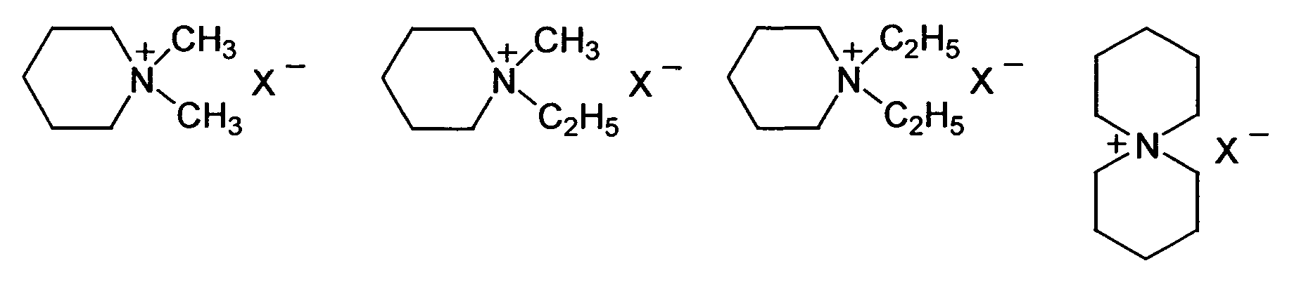 and phosphonium salts such as (CH3)4P+X-, (C2H5)4P+X-,
(C3H7)4P+X-, and (C4H9)4P+X-.
and phosphonium salts such as (CH3)4P+X-, (C2H5)4P+X-,
(C3H7)4P+X-, and (C4H9)4P+X-.
Needless to mention, mixtures of these compounds
may be suitably used.
These compounds are preferably used in
combination with Component (b).
Alternatively, a redox ordinary-temperature
melting salt may be used as Component (c). The term
"redox ordinary-temperature melting salt" denotes a
solvent-free salt comprising only ion pairs, in a
melted state (liquid state) at ordinary temperature,
more specifically denotes a salt comprising ion pairs
which salt has a melting point of 20 °C or below and
will be in a liquid state at a temperature exceeding
20 °C and are capable of inducing a reversible
electrochemical oxidation-reduction reaction. When
the redox ordinary-temperature melting salt is used as
Component (c) , Component (b) may or may not be used in
combination.
One type of the redox ordinary-temperature
melting salts may be used alone or alternatively two
or more types of the salts may be used in the form of
a mixture.
Examples of the redox ordinary-temperature
melting salt include those represented by the following
formulas:
 wherein R is an alkyl group having 2 to 20, preferably
2 to 10 carbon atoms and X- is a halogen ion or SCN-;
wherein R is an alkyl group having 2 to 20, preferably
2 to 10 carbon atoms and X- is a halogen ion or SCN-;
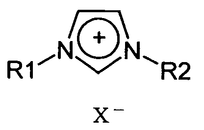 wherein R1 and R2 are each independently an alkyl group
having 1 to 10 carbon atoms, preferably methyl or ethyl
or an aralkyl group having 7 to 20, preferably 7 to 13
carbon atoms, preferably benzyl and may be the same or
different from each other and X- is a halogen ion or
SCN-;
wherein R1 and R2 are each independently an alkyl group
having 1 to 10 carbon atoms, preferably methyl or ethyl
or an aralkyl group having 7 to 20, preferably 7 to 13
carbon atoms, preferably benzyl and may be the same or
different from each other and X- is a halogen ion or
SCN-;
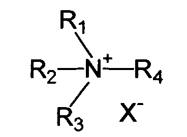 wherein R1, R2, R3, and R4 are each independently an alkyl
group having one or more carbon atoms, preferably 1 to
6 carbon atoms, an aryl group having 6 to 12 carbon atoms
such as phenyl, or a methoxymethyl group and may be the
same or different from each other and X- is a halogen
ion or SCN-.
wherein R1, R2, R3, and R4 are each independently an alkyl
group having one or more carbon atoms, preferably 1 to
6 carbon atoms, an aryl group having 6 to 12 carbon atoms
such as phenyl, or a methoxymethyl group and may be the
same or different from each other and X- is a halogen
ion or SCN-.
No particular limitation is imposed on the amount
of Component (c). Component (c) may be generally
contained in an amount of usually 0.1 percent by mass
or more, preferably 1 percent by mass or more, and more
preferably 10 percent by mass or more and 70 percent
by mass or less, preferably 60 percent by mass or less,
more preferably 50 percent by mass or less, in the
polymeric solid electrolyte.
When Component (c) is used in combination with
Component (b), the mix ratio is desirously selected
such that Component (c) is dissolved in Component (b)
and does not precipitate after being formed into the
polymeric solid electrolyte. The mix ratio by mass of
Component (c)/Component (b) is in the range of
preferably 0.01 to 0.5 and more preferably 0.03 to 0.3.
The mass ratio of Component (a)/(Components (b)
and (c)) is within the range of preferably 1/20 to 1/1,
more preferably 1/10 to 1/2.
No particular limitation is imposed on the amount
of the supporting electrolyte (Component (d)) to be
used. The supporting electrolyte may be contained in
an amount of usually 0.1 percent by mass or more,
preferably 1 percent by mass or more, and more
preferably 10 percent by mass or more and 70 percent
by mass or less, preferably 60 percent by mass or less,
and more preferably 50 percent by mass or less, in the
polymeric solid electrolyte.
The polymeric solid electrolyte may further
contain other components. Examples of other
components include ultraviolet adsorbing agents and
amine compounds. No particular limitation is imposed
on eligible ultraviolet adsorbing agent. Typical
examples of the ultraviolet adsorbing agent include
organic ultraviolet adsorbing agents such as compounds
having a benzotriazole molecule structure or a
benzophenone molecule structure.
Examples of the compound having a benzotriazole
molecule structure include those represented by
formula (1) below:

In formula (1), R81 is hydrogen, halogen or an
alkyl group having 1 to 10, preferably 1 to 6 carbon
atoms. Specific examples of the halogen are fluorine,
chlorine, bromine, and iodine. Specific examples of
the alkyl group include methyl, ethyl, propyl, i-propyl,
butyl, t-butyl and cyclohexyl groups. R81 is usually
substituted at the 4- or 5-position of the
benzotriazole ring but the halogen and the alkyl group
are usually located at the 4-position. R82 is hydrogen
or an alkyl group having 1 to 10, preferably 1 to 6 carbon
atoms. Examples of the alkyl group include methyl,
ethyl, propyl, i-propyl, butyl, t-butyl, and
cyclohexyl groups. R83 is an alkylene or alkylidene
group having 1 to 10, preferably 1 to 3 carbon atoms.
Examples of the alkylene group include methylene,
ethylene, trimethylene, and propylene groups.
Examples of the alkylidene group include ethylidene and
propylidene groups.
Specific examples of the compounds represented by
formula (1) include
3-(5-chloro-2H-benzotriazole-2-yl)-5-(1,1-dimethylethyl)-4-hydroxy-benzene
propanoic acid,
3-(2H-benzotriazole-2-yl)-5-(1,1-dimethylethyl)-4-hydroxy-benzene
ethanoic acid,
3-(2H-benzotriazole-2-yl)-4-hydroxybenzene ethanoic
acid,
3-(5-methyl-2H-benzotriazole-2-yl)-5-(1-methylethyl)-4-hydroxybenzene
propanoic acid,
2-(2'-hydroxy-5'-methylphenyl)benzotriazole,
2-[2'-hydroxy-3',5'-bis(α,α-dimethylbenzyl)
phenyl] benzotriazole, 2-(2'-hydroxy-3',
5'-di-t-butylphenyl)benzotriazol,
2-(2'-hydroxy-3'-t-butyl-5'-methylphenyl)-5-chloro
benzotriazole, and
3-(5-chloro-2H-benzotriazole-2-yl)-5-(1,1-dimethyl
ethyl)-4-hydroxy-benzene propanoic acid octylester.
Specific examples of the compound having a
benzophenone molecule structure include those
represented by the following formulas:

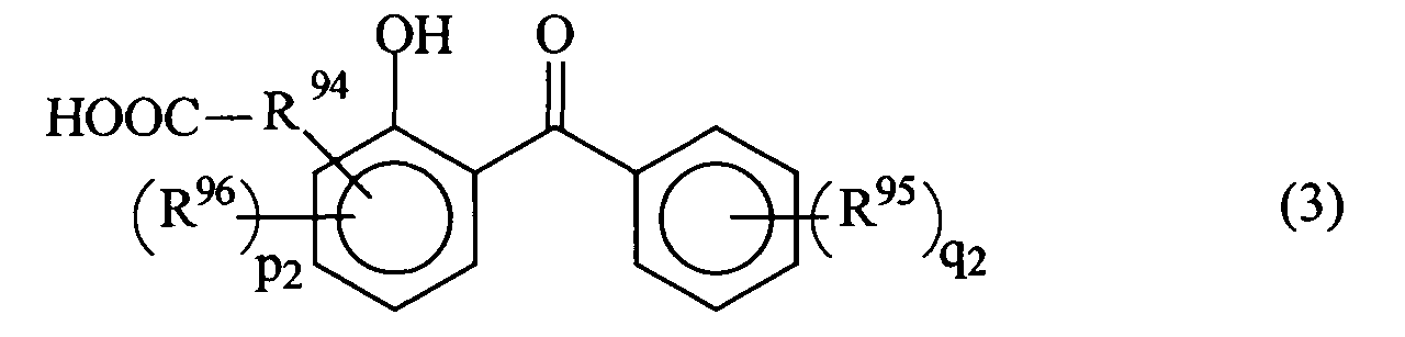

In formulas (2) to (4), R92, R93, R95, R96, R98, and
R99 may be the same or different from each other and
are each independently a hydroxyl group or an alkyl or
alkoxy group having 1 to 10, preferably 1 to 6 carbon
atoms. Examples of the alkyl group include methyl,
ethyl, propyl, i-propyl, butyl, t-butyl, and
cyclohexyl groups. Specific examples of the alkoxy
group are methoxy, ethoxy, propoxy, i-propoxy, and
butoxy groups.
R91, R94, and R97 are each independently an alkylene
or alkylidene group having 1 to 10, preferably 1 to 3
carbon atoms. Examples of the alkylene group include
methylene, ethylene, trimethylene, and propylene
groups. Examples of the alkylidene group include
ethylidene and propylidene groups.
In the above formulas, p1, p2, p3, q1, q2, and q3
are each independently an integer of 0 to 3.
Preferred examples of the compounds having a
benzophenone molecule structure, represented by
formulas (2) to (4) include
2-hydroxy-4-methoxybenzophenone-5-carboxylic acid,
2,2'-dihydroxy-4-methoxybenzophenone-5-carboxylic
acid, 4-(2-hydroxybenzoyl)-3-hydroxybenzen propanoic
acid, 2,4-dihydroxybenzophenone,
2-hydroxy-4-methoxybenzophenone,
2-hydroxy-4-methoxybenzophenone-5-sulfonic acid,
2-hydroxy-4-n-octoxybenzophenone,
2,2'-dihydroxy-4,4'-dimethoxybenzophenone,
2,2',4,4'-tetrahydroxybenzophenone, and
2-hydroxy-4-methoxy-2'-carboxybenzophenone.
Needless to mention, two or more of these
ultraviolet adsorbing agents may be used in
combination.
The use of the ultraviolet adsorbing agent is
optional. No particular limitation is imposed on the
amount of the ultraviolet adsorbing agent to be used.
However, if the agent is used, it may be contained in
an amount of 0.1 percent by mass or more, preferably
1 percent by mass or more and 20 percent by mass or less
and preferably 10 percent by mass or less, in the
polymeric solid electrolyte.
No particular limitation is imposed on amine
compounds which the polymeric solid electrolyte may
contain. Various aliphatic and aromatic amines can be
used. Typical examples of the amine compound include
pyridine derivatives, bipyridine derivatives, and
quinoline derivatives. It is expected that the
open-circuit voltage is enhanced by addition of these
amine compounds. Specific examples of these compounds
include 4-t-butyl-pyridine, quinoline, and
isoquinoline.
In the present invention, the electrolyte may be
produced as a redox electrolyte film, and the method
for producing the same will be described next.
The redox electrolyte film may be obtained by
forming a mixture of Components (a) and (c) and optional
components to be added if necessary into a film by a
conventional method. No particular limitation is
imposed on the film forming method, which, therefore,
may be any of extrusion, casting, spin-coating, and
dip-coating methods.
Extrusion may be conducted in a conventional
manner wherein the mixture of the above-described
components is formed into a film after being
heat-melted.
Casting is conducted by adjusting the viscosity
of the mixture by adding thereto a suitable diluent,
and coating and drying the diluted mixture with a
conventional coater normally used for casting thereby
forming the mixture into a film. Examples of the coater
include doctor coaters, blade coaters, rod coaters,
knife coaters, reverse roll coaters, gravure coaters,
spray coaters, and curtain coaters among which a
suitable one is selected depending on the viscosity and
film thickness.
Spin coating is conducted by adjusting the
viscosity of the mixture by adding a suitable diluent,
and coating and drying the diluted mixture with a
commercially available spin-coater thereby forming the
mixture into a film.
Dip coating is conducted by adjusting the
viscosity of the mixture by adding a suitable diluent
so as to obtain a solution of the mixture, dipping and
lifting a suitable substrate therein, and drying the
substrate thereby forming the mixture into a film.
No particular limitation is imposed on the
semiconductor layer to be used in the photovoltaic
device of the present invention. Examples of the
semiconductor layer include those of Bi2S3, CdS, CdSe,
CdTe, CuInS2, CuInSe2, Fe2O3, GaP, GaAs, InP, Nb2O5, PbS,
Si, SnO2, TiO2, WO3, ZnO, and ZnS, among which preferred
are those of CdS, CdSe, CuInS2, CuInSe2, Fe2O3, GaAs,
InP, Nb2O5, PbS, SnO2, TiO2, WO3, and ZnO. These
materials may be used in combination. Particularly
preferred are those of TiO2, ZnO, SnO2, and Nb2O5, while
most preferred are those of TiO2 and ZnO.
The semiconductor used in the present invention
may be monocrystalline or polycrystalline. For
example, the crystal system may be selected from those
of anatase, rutile, or brookite type among which
preferred are those of anatase type. The semiconductor
layer may be formed by any suitable conventional
method.
The semiconductor layer may be obtained by coating
a nanoparticle dispersant or sol solution, of the
above-mentioned semiconductor on the substrate by any
conventional method. No particular limitation is
imposed on the coating method. Therefore, the coating
may be conducted by a method wherein the semiconductor
is obtained in the form of film by casting;
spin-coating; dip-coating; bar-coating; and various
printing methods such as screen-printing.
The thickness of the semiconductor layer may be
arbitrarily selected but is 0.5 µm or more and 50 µm
or less, and preferably 1 µm or more and 20 µm or
less.
For purpose of enhancing the light-absorbing
efficiency of the semiconductor layer, various dyes may
be adsorbed to or contained in the layer.
No particular limitation is imposed on the dye to
be used in the present invention as long as it can
enhance the light-absorbing efficiency of the
semiconductor layer. One or more of various metal
complex dyes or organic dyes may be usually used. In
order to improve the adsorptivity to the semiconductor
layer, dyes having in their molecules a functional
group such as carboxyl, hydroxyl, sulfonyl, phosphonyl,
carboxylalkyl, hydroxyalkyl, sulfonylalkyl, and
phosphonylalkyl groups are preferably used.
Eligible metal complex dyes are a complex of
ruthenium, osmium, iron, cobalt, or zinc; metal
phthalocyanine; and chlorophyll.
Examples of the metal complex dyes used in the
present invention include those represented by the
following formulas:
 wherein X is a univalent anion and two X may be
independent of each other or cross-linked and are any
of those represented by the following formulas:
wherein X is a univalent anion and two X may be
independent of each other or cross-linked and are any
of those represented by the following formulas:

 wherein X is a univalent anion and may be any of those
represented by the following formulas:
wherein X is a univalent anion and may be any of those
represented by the following formulas:

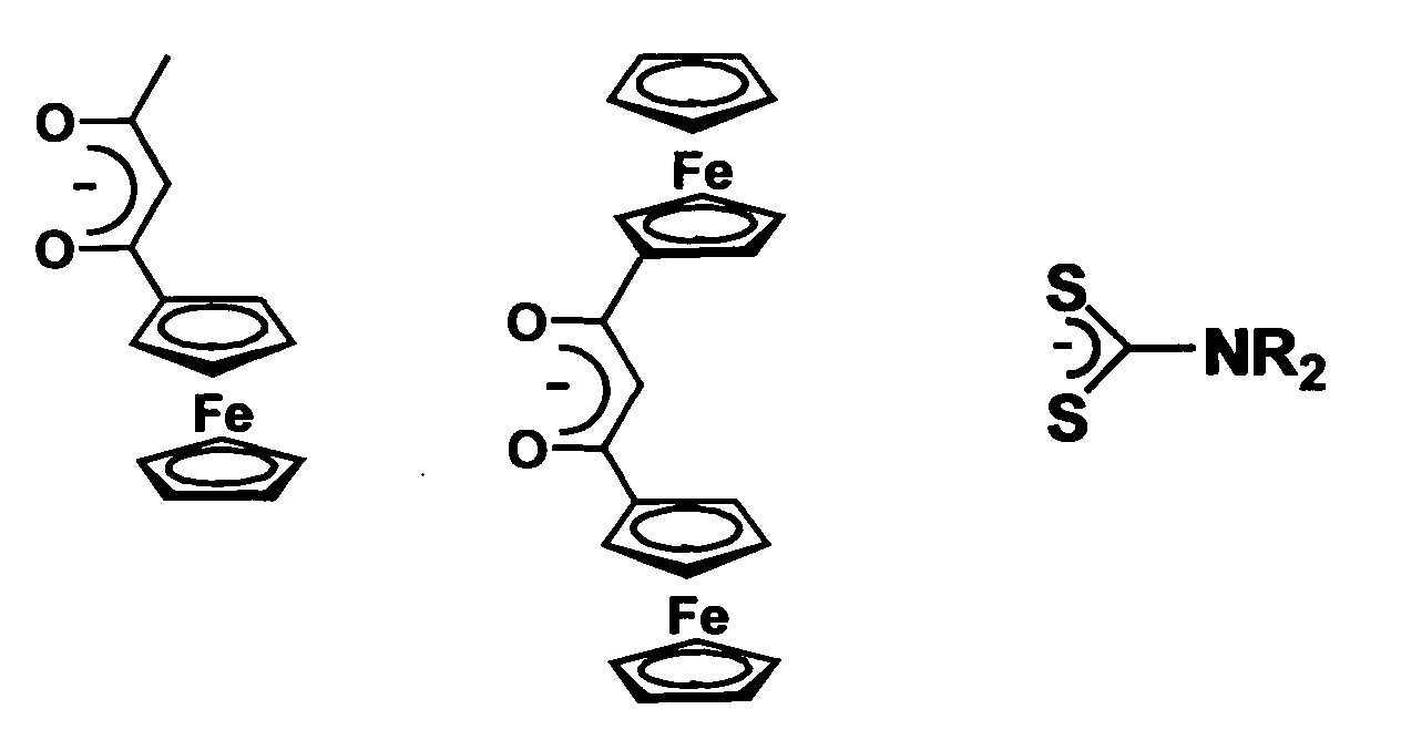 wherein Y is a univalent anion and may be any of halogen
ions, SCN-, ClO4 -, BF4 -, CF3SO3 -, (CF3SO2)2N-, (C2F5SO2)2N-,
PF6 -, AsF6 -, CH3COO-, CH3(C6H4)SO3 -, and (C2F5SO2)3C-;
wherein Y is a univalent anion and may be any of halogen
ions, SCN-, ClO4 -, BF4 -, CF3SO3 -, (CF3SO2)2N-, (C2F5SO2)2N-,
PF6 -, AsF6 -, CH3COO-, CH3(C6H4)SO3 -, and (C2F5SO2)3C-;
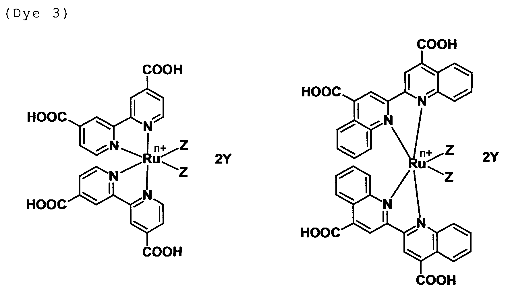 wherein Z is an atomic group having an unshared electron
pair, and two Z may be independent of each other or
cross-linked and any of those represented by the
following formulas:
wherein Z is an atomic group having an unshared electron
pair, and two Z may be independent of each other or
cross-linked and any of those represented by the
following formulas:
 and Y is an univalent anion and may be any of halogen
ions, SCN-, ClO4 -, BF4 -, CF3SO3 -, (CF3SO2)2N-, (C2F5SO2)2N-,
PF6 -, AsF6 -, CH3COO-, CH3(C6H4)SO3 -, and (C2F5SO2)3C-; and
and Y is an univalent anion and may be any of halogen
ions, SCN-, ClO4 -, BF4 -, CF3SO3 -, (CF3SO2)2N-, (C2F5SO2)2N-,
PF6 -, AsF6 -, CH3COO-, CH3(C6H4)SO3 -, and (C2F5SO2)3C-; and
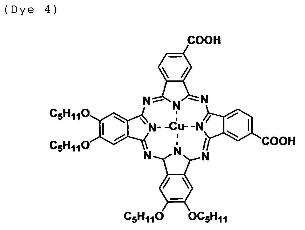
Eligible organic dyes are cyanine-based dyes,
hemicyanine-based dyes, merocyanine-based dyes,
xanthene-based dyes, triphenylmethane-based dyes, and
metal-free phthalocyanine-based dyes.
Examples of the dyes used in the present invention
include those represented by the following formulas:


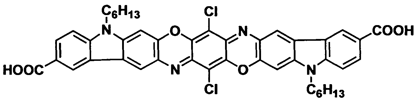


The dye may be adsorbed to the semiconductor layer
on a transparent electrically conductive substrate by
coating a solution obtained by dissolving the dye in
a solvent on the semiconductor layer by spray- or
spin-coating and drying the solution. In this case,
the substrate may be heated to a suitable temperature.
Alternatively, the dye may be adsorbed to the
semiconductor layer by dipping the layer into the
solution. No particular limitation is imposed on the
time for dipping as long as the dye is sufficiently
adsorbed to the semiconductor layer. The substrate is
dipped into the solution for preferably 1 to 30 hours,
particularly preferably 5 to 20 hours. If necessary,
the solvent or the substrate may be heated upon dipping.
The concentration of the dye in the solution is
preferably from 1 to 1,000 mM/L and more preferably from
10 to 500 mM/L.
No particular limitation is imposed on the solvent
to be used as long as it dissolves the dye but not the
semiconductor layer. Examples of the solvent include
alcohols such as methanol, ethanol, 1-propanol,
2-propanol, 1-butanol, 2-butanol, and t-butanol,
nitrile-based solvents such as acetonitrile,
propionitrile, methoxypropionitrile, and
glutaronitrile, benzene, toluene, o-xylene, m-xylene,
p-xylene, pentane, heptane, hexane, cyclohexane,
heptane, ketones such as acetone, methyl ethyl ketone,
diethyl ketone, and 2-butanone, diethylether,
tetrahydrofuran, ethylene carbonate, propylene
carbonate, nitromethane, dimethylformamide,
dimethylsulfoxide, hexamethylphosphoamide,
dimethoxyethane, γ-butyrolactone, γ-valerolactone,
sulfolane, adiponitrile, methoxyacetonitrile,
dimethylacetoamide, methylpyrrolidinone, dioxolan,
trimethyl phosphate, triethyl phosphate, tripropyl
phosphate, ethyldimethyl phosphate, tributyl
phosphate, tripentyl phosphate, trihexyl phosphate,
triheptyl phosphate, trioctyl phosphate, trinonyl
phosphate, tridecyl phosphate,
tris(trifluoromethyl)phosphate,
tris(pentafluoroethyl)phosphate,
triphenylpolyethylene glycol phosphate, and
polyethylene glycol.
The transparent electrically conductive
substrate (hereinafter referred to as "transparent
conductive substrate") will be described next.
The transparent conductive substrate is produced
by laminating a transparent electrode layer over a
transparent substrate. No particular limitation is
imposed on the transparent substrate. The material,
thickness, size, and shape of the substrate can be
properly selected depending on the purposes. For
example, the substrate may be selected from colored or
colorless glasses, wire-reinforced glasses, glass
blocks, and colored or colorless transparent resins.
Specific examples are polyesters such as polyethylene
terephthalate, polyamides, polysulfones,
polyethersulfones, polyether ether ketones,
polyphenylene sulfides, polycarbonates, polyimides,
polymethyl methacrylates, polystyrenes, cellulose
triacetates, and polymethyl pentenes. The term
"transparent" used herein denotes a transmissivity of
10 to 100 percent. The substrates used herein are those
having a smooth surface at ordinary temperature, which
surface may be flat or curved or deformed with stress.
No particular limitation is imposed on the
transparent electrode layer acting as an electrode as
long as it can achieve the purposes of the present
invention. For example, the layer may be a thin metal
film of gold, silver, chromium, copper, or tungsten or
an electrically conductive film made of a metal oxide.
Preferred examples of the metal oxide include those
obtained by doping to tin oxide or zinc oxide trace
amounts of components such as Indium Tin Oxide (ITO
(In2O3:Sn)), Fluorine doped Tin Oxide (FTO (SnO2:F)),
and Aluminum doped Zinc Oxide (AZO (ZnO:Al)).
The film thickness is usually from 10 nm to 10 µm,
preferably from 100 nm to 2 µm. The surface
resistance (resistivity) is properly selected
depending on the use of the substrate in the present
invention, but is usually from 0.5 to 500 Ω/sq,
preferably from 2 to 50 Ω/sq.
The photovoltaic device of the present invention
may be used as a photovoltaic device having a
cross-section as shown in Fig. 1. The device has a
substrate A composed of a transparent substrate and a
semiconductor layer (titania and dye layers) formed
thereon and a conductive counter electrode (substrate
B) composed of a substrate and a conductive carbon layer
formed thereon. The space defined between the
substrates A and B is filled with an electrolytes, and
the peripheral space of the device is sealed with a
sealant. Lead wires (not shown) are connected to the
electrically conductive portions of substrates A and
B to take out electromotive force.
No particular limitation is imposed on the method
of producing the photovoltaic device of the present
invention. In general, the photovoltaic device can be
easily produced by a conventional method wherein the
substrates A and B are sealed at their periphery and
joined to each other with a predetermined space
therebetween, and an electrolyte is put thereinto. The
space between the substrates is generally 0.1 µm or
larger and preferable 1 µm or larger and generally up
to 1 mm and preferably 0.5 mm or smaller.
A photovoltaic device with excellent durability
can be provided at inexpensive material and production
costs, using the counter electrode of the present
invention. The resulting device is suitable for the
use in solar batteries.
The present invention will be described in more
detail with reference to the following examples but are
not limited thereto.
To 10 g of a thermosetting acrylic resin (product
name "Acrydic" manufactured by DAINIPPON INK AND
CHEMICALS, INCORPORATED) and 2.2 g of a melamine resin
(product name "Bansemin" manufactured by Harima
Chemicals, Inc.) were added 12 g of graphite (product
name "USSP" manufactured by Nippon Graphite Industries,
Ltd.). 24 g of ethylene glycol mono-n-butyl ether were
added to and mixed with the mixture thereby preparing
a conductive paste.
The resulting conductive paste was bar-coated
substantially over the entire surface of a 5 cm square
glass substrate and heat-cured at a temperature of
160 °C for 0.5 hour. Thereafter, the cured paste was
calcined under a nitrogen atmosphere at a temperature
of 500 °C for 3 hours thereby obtaining a counter
electrode having a conductive carbon layer. The
thickness and surface resistance of the carbon layer
was 50 µm and 50 Ω/sq, respectively.
Ti-Nanoxide T manufactured by SOLARONIX was
bar-coated over a 5 cm square SnO2:F glass (transparent
conductive glass obtained by forming an SnO2:F film on
a glass substrate) with a film resistivity of 30 Ω/sq
and dried. When the transparent conductive glass
substrate was bar-coated, some pieces of Scotch-tape
were attached to the 5 mm-width sides of the glass such
that the thickness of the Ti-Nanoxide T was made uniform.
The coated substrate was calcined at a temperature of
500 °C for 30 minutes. The substrate was dipped into
a ruthenium dye represented by the formula below
/ethanol solution (3.0 x 10⁻⁴ mol/L) for 15 hours thereby
forming a dye layer. The resulting glass substrate and
the counter electrode obtained above were joined
together. A propylene carbonate solution containing
0.3 mol/L lithium iodine and 0.03 mol/L iodine was
infiltrated by capillary phenomenon to the contact
portions of the substrate and the counter electrode,
and the peripheries therebetween were sealed with an
epoxy sealant. Lead wires were connected to the
conductive layer portion of the transparent conductive
substrate and the counter electrode.
A simulated sunlight was irradiated to the
resulting cell so as to measure the current voltage
characteristics. It was confirmed that the cell
exhibited excellent photoelectric conversion
characteristics as shown in Fig. 2.

To 48 g of a thermosetting acrylic resin (product
name "Acryl-G" manufactured by HONNY CHEMICAL CO.,
LTD. ) and 10 g of a melamine resin (product name "NIKALAC
SM551" manufactured by Sanwa Chemical Co., Ltd.) were
added 10 g of ketjen black (product name "ECP600JD"
manufactured by MITSUBISHI CHEMICAL CORPORATION). 80
g of ethylene glycol mono-n-butyl ether were added to
and mixed with the mixture thereby preparing a
conductive paste.
The resulting conductive paste was bar-coated
substantially over the entire surface of a 5 cm square
glass substrate and heat-cured at a temperature of
160 °C for 0.5 hour. Thereafter, the cured paste was
calcined under a nitrogen atmosphere at a temperature
of 500 °C for 3 hours thereby obtaining a counter
electrode having a conductive carbon layer. The
thickness and surface resistance of the carbon layer
was 50 µm and 55 Ω/sq, respectively.
Ti-Nanoxide T manufactured by SOLARONIX was
bar-coated over a 5 cm square SnO2:F glass (transparent
conductive glass obtained by forming an SnO2:F film on
a glass substrate) with a film resistivity of 30 Ω/sq
and dried. When the transparent conductive glass
substrate was bar-coated, some pieces of Scotch-tape
were attached to the 5 mm-width sides of the glass such
that the thickness of the Ti-Nanoxide T was made uniform.
The coated substrate was calcined at a temperature of
500 °C for 30 minutes. The substrate was dipped into
a ruthenium dye (product name "Ruthenium-535-bisTBA"
manufactured by Solaronix) /ethanol solution (5.0 x 10⁻⁴
mol/L) for 15 hours thereby forming a dye layer. The
resulting glass substrate and the counter electrode
obtained above were joined together. A
3-methoxypropionitrile solution containing 0.1 mol/L
lithium iodine, 0.5 mol/L
1-propyl-2,3-dimethylimidazolium iodine, 0.5 mol/L
4-t-butylpyridine and 0.05 mol/L iodine was
infiltrated by capillary phenomenon to the contact
portions of the substrate and the counter electrode,
and the peripheries therebetween were sealed with an
epoxy sealant. Lead wires were connected to the
conductive layer portion of the transparent conductive
substrate and the counter electrode.
A simulated sunlight was irradiated to the
resulting cell so as to measure the current voltage
characteristics. It was confirmed that the cell
exhibited excellent photoelectric conversion
characteristics as shown in Fig. 3.
To 48 g of a thermosetting silicone resin (product
name "RZ-7705" manufactured by Nippon Unicar Company
Limited) were added 10 g of ketjen black (product name
"ECP600JD" manufactured by MITSUBISHI CHEMICAL
CORPORATION). 80 g of ethylene glycol mono-n-butyl
ether were added to and mixed with the mixture thereby
preparing a conductive paste.
The resulting conductive paste was bar-coated
substantially over the entire surface of a 5 cm square
glass substrate and heat-cured at a temperature of
160 °C for 0.5 hour. Thereafter, the cured paste was
calcined under a nitrogen atmosphere at a temperature
of 500 °C for 3 hours thereby obtaining a counter
electrode having a conductive carbon layer. The
thickness and surface resistance of the carbon layer
was 50 µm and 35 Ω/sq, respectively.
Ti-Nanoxide T manufactured by SOLARONIX was
bar-coated over a 5 cm square SnO2:F glass (transparent
conductive glass obtained by forming an SnO2:F film on
a glass substrate) with a film resistivity of 30 Ω/sq
and dried. When the transparent conductive glass
substrate was bar-coated, some pieces of Scotch-tape
were attached to the 5 mm-width sides of the glass such
that the thickness of the Ti-Nanoxide T was made uniform.
The coated substrate was calcined at a temperature of
500 °C for 30 minutes. The substrate was dipped into
a ruthenium dye (product name "Ruthenium-620-1H-3TBA"
manufactured by Solaronix) /ethanol solution (5.0 x 10⁻⁴
mol/L) for 15 hours thereby forming a dye layer. The
resulting glass substrate and the counter electrode
obtained above were joined together. A
3-methoxypropionitrile solution containing 0.1 mol/L
lithium iodine, 0.5 mol/L
1-propyl-2,3-dimethylimidazolium iodine, 0.5 mol/L
4-t-butylpyridine and 0.05 mol/L iodine was
infiltrated by capillary phenomenon to the contact
portions of the substrate and the counter electrode,
and the peripheries therebetween were sealed with an
epoxy sealant. Lead wires were connected to the
conductive layer portion of the transparent conductive
substrate and the counter electrode.
A simulated sunlight was irradiated to the
resulting cell so as to measure the current voltage
characteristics. It was confirmed that the cell
exhibited excellent photoelectric conversion
characteristics as shown in Fig. 4.
Claims (5)
- A photovoltaic device wherein it has a counter electrode comprising a substrate and an electrically conductive carbon layer formed thereon.
- A photovoltaic device comprising at least a transparent electrically conductive substrate, a semiconductor layer formed thereon, an electrolyte layer, a substrate, and an electrically conductive carbon layer formed thereon.
- The photovoltaic device according claim 1 or 2, wherein said substrate is an electrically conductive substrate.
- The photovoltaic device according claim 2, wherein said electrolyte layer is a polymeric solid electrolyte layer.
- The photovoltaic device according claim 2, wherein said semiconductor layer contains a dye.
Applications Claiming Priority (3)
| Application Number | Priority Date | Filing Date | Title |
|---|---|---|---|
| JP2002163482 | 2002-06-04 | ||
| JP2002163482 | 2002-06-04 | ||
| PCT/JP2003/006819 WO2003103085A1 (en) | 2002-06-04 | 2003-05-30 | Photoelectric transducer |
Publications (2)
| Publication Number | Publication Date |
|---|---|
| EP1511116A1 true EP1511116A1 (en) | 2005-03-02 |
| EP1511116A4 EP1511116A4 (en) | 2010-05-05 |
Family
ID=29706634
Family Applications (1)
| Application Number | Title | Priority Date | Filing Date |
|---|---|---|---|
| EP03730713A Withdrawn EP1511116A4 (en) | 2002-06-04 | 2003-05-30 | PHOTOELECTRIC TRANSDUCER |
Country Status (4)
| Country | Link |
|---|---|
| US (1) | US20050092359A1 (en) |
| EP (1) | EP1511116A4 (en) |
| JP (1) | JPWO2003103085A1 (en) |
| WO (1) | WO2003103085A1 (en) |
Cited By (1)
| Publication number | Priority date | Publication date | Assignee | Title |
|---|---|---|---|---|
| DE112010001803B4 (en) * | 2009-04-30 | 2018-02-08 | The Yokohama Rubber Co., Ltd. | Electrolyte for dye-sensitized solar cells and dye-sensitized solar cell using the electrolyte |
Families Citing this family (23)
| Publication number | Priority date | Publication date | Assignee | Title |
|---|---|---|---|---|
| DE102004036793A1 (en) * | 2004-07-29 | 2006-03-23 | Konarka Technologies, Inc., Lowell | Nanoporous fullerene layers and their use in organic photovoltaics |
| EP1672653B1 (en) | 2004-12-20 | 2019-07-17 | Merck Patent GmbH | Patterned photovoltaic cell |
| JP2006244919A (en) * | 2005-03-04 | 2006-09-14 | Nippon Oil Corp | Photoelectric conversion element |
| JP4932200B2 (en) * | 2005-09-08 | 2012-05-16 | 株式会社フジクラ | Electrode, manufacturing method thereof, and photoelectric conversion element |
| KR101174887B1 (en) * | 2006-01-20 | 2012-08-17 | 삼성에스디아이 주식회사 | A counter electrode for photovoltaic cell using supported catalyst |
| DE102006023638A1 (en) * | 2006-05-18 | 2007-11-22 | Sefar Ag | Photovoltaic cell |
| US20080001141A1 (en) * | 2006-06-28 | 2008-01-03 | Unidym, Inc. | Doped Transparent and Conducting Nanostructure Networks |
| KR20080006735A (en) * | 2006-07-13 | 2008-01-17 | 삼성전자주식회사 | Solar cell using catalyst supported carbon nanotube and manufacturing method thereof |
| WO2008066933A2 (en) | 2006-12-01 | 2008-06-05 | The Regents Of The University Of California | Enhancing performance characteristics of organic semiconducting films by improved solution processing |
| JP2009048946A (en) * | 2007-08-22 | 2009-03-05 | Teijin Dupont Films Japan Ltd | Dye-sensitized photoelectric conversion element |
| CN101842905B (en) * | 2007-08-28 | 2013-01-16 | 3G太阳能光电有限公司 | Photovoltaic dye cells with improved auxiliary electrodes |
| US7910015B2 (en) * | 2007-10-22 | 2011-03-22 | Institute Of Nuclear Energy Research | Polymer electrolyte for dye sensitized solar cell |
| US8227691B2 (en) * | 2007-10-31 | 2012-07-24 | The Regents Of The University Of California | Processing additives for fabricating organic photovoltaic cells |
| US20090194167A1 (en) * | 2008-02-05 | 2009-08-06 | Konarka Technologies, Inc. | Methods of Forming Photoactive Layer |
| JP5219538B2 (en) * | 2008-02-12 | 2013-06-26 | 大成建設株式会社 | Solar cell with photovoltaic thin film directly formed on substrate |
| FR2932009B1 (en) * | 2008-06-02 | 2010-09-17 | Saint Gobain | PHOTOVOLTAIC CELL AND PHOTOVOLTAIC CELL SUBSTRATE |
| JP5273709B2 (en) * | 2008-07-02 | 2013-08-28 | シャープ株式会社 | Dye-sensitized solar cell, method for producing the same, and dye-sensitized solar cell module |
| KR100997843B1 (en) * | 2008-08-29 | 2010-12-01 | 주식회사 솔켐 | Dye-sensitized solar cell device including polymer electrolyte manufactured by electrospinning method and method for manufacturing same |
| KR101033304B1 (en) | 2009-02-09 | 2011-05-09 | 광주과학기술원 | Organic solar cell having luminescent properties and manufacturing method |
| KR101131055B1 (en) | 2010-07-09 | 2012-03-30 | 포항공과대학교 산학협력단 | Dye sensitized solar cell comprising counter electrode having mesoporous carbon electrode deposited on transparent substrate and preparation method thereof |
| WO2014150235A1 (en) * | 2013-03-15 | 2014-09-25 | The Trustees Of Dartmouth College | Multifunctional nanostructured metal-rich metal oxides |
| KR20140122361A (en) * | 2013-04-09 | 2014-10-20 | 삼성에스디아이 주식회사 | Electrolyte for dye sensitized solar cell and dye sensitized solar cell using the same |
| KR101728329B1 (en) | 2015-11-19 | 2017-05-02 | 현대자동차주식회사 | Touch control device, vehicle comprising the same, and manufacturing method thereof |
Family Cites Families (18)
| Publication number | Priority date | Publication date | Assignee | Title |
|---|---|---|---|---|
| JP2955646B2 (en) * | 1996-09-12 | 1999-10-04 | 工業技術院長 | Organic dye-sensitized oxide semiconductor electrode and solar cell including the same |
| JPH11329519A (en) * | 1998-04-27 | 1999-11-30 | Minnesota Mining & Mfg Co <3M> | Photocell |
| JP2000036331A (en) * | 1998-07-16 | 2000-02-02 | Konica Corp | Metal oxide, semiconductor, electrode for photoelectric conversion material, and solar battery |
| JP3945038B2 (en) * | 1998-09-21 | 2007-07-18 | 松下電器産業株式会社 | Dye-sensitized solar cell |
| JP3544888B2 (en) * | 1999-03-31 | 2004-07-21 | 株式会社東芝 | Photosensitized solar cell |
| US6291763B1 (en) * | 1999-04-06 | 2001-09-18 | Fuji Photo Film Co., Ltd. | Photoelectric conversion device and photo cell |
| ATE531722T1 (en) * | 1999-04-26 | 2011-11-15 | Fujifilm Corp | RUTHENIUM COMPLEX DYE |
| JP4129103B2 (en) * | 1999-09-09 | 2008-08-06 | Tdk株式会社 | Dye-coupled electrode for dye-sensitized solar cell and dye-sensitized solar cell using the same |
| JP3430254B2 (en) * | 2000-03-13 | 2003-07-28 | 独立行政法人産業技術総合研究所 | Metal complex having β-diketonate, method for producing the same, photoelectric conversion element, and photochemical cell |
| JP4415482B2 (en) * | 2000-03-28 | 2010-02-17 | パナソニック電工株式会社 | Photoelectric conversion element |
| JP4632492B2 (en) * | 2000-07-26 | 2011-02-16 | 日本化薬株式会社 | Semiconductor electrode |
| EP1180774B1 (en) * | 2000-08-15 | 2006-10-11 | Fuji Photo Film Co., Ltd. | Photoelectric conversion device and method for producing same |
| JP4659954B2 (en) * | 2000-09-19 | 2011-03-30 | 大日本印刷株式会社 | Method for producing dye-sensitized solar cell and method for producing dye-sensitized solar cell module |
| JP2002100419A (en) * | 2000-09-25 | 2002-04-05 | Mitsubishi Chemicals Corp | Photoelectric conversion element |
| EP1207572A1 (en) * | 2000-11-15 | 2002-05-22 | Dr. Sugnaux Consulting | Mesoporous electrodes for electrochemical cells and their production method |
| US6677516B2 (en) * | 2001-01-29 | 2004-01-13 | Sharp Kabushiki Kaisha | Photovoltaic cell and process for producing the same |
| JP2002298936A (en) * | 2001-03-30 | 2002-10-11 | Fuji Xerox Co Ltd | Photoelectric conversion element and its manufacturing method |
| JP4320138B2 (en) * | 2001-10-31 | 2009-08-26 | 独立行政法人科学技術振興機構 | A solid dye-sensitized solar cell in which a counter electrode of a dye-sensitized solar cell using a polymer solid electrolyte as a hole transport layer is formed of a material composed of an electron conductive material and a polymer electrolyte. |
-
2003
- 2003-05-30 JP JP2004510062A patent/JPWO2003103085A1/en active Pending
- 2003-05-30 EP EP03730713A patent/EP1511116A4/en not_active Withdrawn
- 2003-05-30 WO PCT/JP2003/006819 patent/WO2003103085A1/en not_active Ceased
-
2004
- 2004-11-24 US US10/996,837 patent/US20050092359A1/en not_active Abandoned
Cited By (1)
| Publication number | Priority date | Publication date | Assignee | Title |
|---|---|---|---|---|
| DE112010001803B4 (en) * | 2009-04-30 | 2018-02-08 | The Yokohama Rubber Co., Ltd. | Electrolyte for dye-sensitized solar cells and dye-sensitized solar cell using the electrolyte |
Also Published As
| Publication number | Publication date |
|---|---|
| WO2003103085A1 (en) | 2003-12-11 |
| EP1511116A4 (en) | 2010-05-05 |
| US20050092359A1 (en) | 2005-05-05 |
| JPWO2003103085A1 (en) | 2005-10-06 |
Similar Documents
| Publication | Publication Date | Title |
|---|---|---|
| EP1511116A1 (en) | Photoelectric transducer | |
| EP1696053B1 (en) | Nano-array electrode manufacturing method and photoelectric converter using same | |
| JP5096064B2 (en) | Dye-sensitized solar cell module | |
| JP4528082B2 (en) | Electrode substrate having conductive pattern and solar cell | |
| KR20140009967A (en) | Additive for electrolytic composition, electrolytic composition using this additive, and dye-sensitized solar cell | |
| JP4071428B2 (en) | Dye-sensitized solar cell and method for producing the same | |
| JP4948029B2 (en) | Dye-sensitized solar cell | |
| EP1494308B1 (en) | Photoelectric conversion element | |
| JP5000162B2 (en) | Dye-sensitized solar cell | |
| JP5540744B2 (en) | Photoelectric conversion element | |
| JP2006324111A (en) | Flexible dye-sensitized solar cell | |
| JP2006134827A (en) | Electrode and dye-sensitized solar cell | |
| JP2005044697A (en) | Photoelectric conversion element | |
| JP2005150278A (en) | Electrode and functional element | |
| JP2006261089A (en) | Dye-sensitized solar cell element | |
| JP2006244919A (en) | Photoelectric conversion element | |
| JP4931402B2 (en) | Photoelectric conversion element | |
| JP4648635B2 (en) | Method for manufacturing photoelectric conversion element | |
| US20050098206A1 (en) | Photoelectric converting device | |
| JP4849844B2 (en) | Dye-sensitized solar cell | |
| JP6445378B2 (en) | Photoelectric conversion element | |
| JP4778217B2 (en) | Electrode substrate and dye-sensitized solar cell | |
| JP4947951B2 (en) | Titanium oxide electrode, method for producing the same, and photoelectric conversion element | |
| JP2005044696A (en) | Photoelectric conversion element | |
| JP2004071326A (en) | Manufacturing method of photoelectric conversion element, photoelectric conversion element and photoelectric cell |
Legal Events
| Date | Code | Title | Description |
|---|---|---|---|
| PUAI | Public reference made under article 153(3) epc to a published international application that has entered the european phase |
Free format text: ORIGINAL CODE: 0009012 |
|
| 17P | Request for examination filed |
Effective date: 20041125 |
|
| AK | Designated contracting states |
Kind code of ref document: A1 Designated state(s): AT BE BG CH CY CZ DE DK EE ES FI FR GB GR HU IE IT LI LU MC NL PT RO SE SI SK TR |
|
| A4 | Supplementary search report drawn up and despatched |
Effective date: 20100409 |
|
| 17Q | First examination report despatched |
Effective date: 20101110 |
|
| STAA | Information on the status of an ep patent application or granted ep patent |
Free format text: STATUS: THE APPLICATION IS DEEMED TO BE WITHDRAWN |
|
| 18D | Application deemed to be withdrawn |
Effective date: 20110323 |