-
The invention relates to integrated CMOS light sensing
arrays comprising light sensing cells, and in particular to the
structure of the light sensing cells.
-
CMOS light sensing arrays integrated on chips are
widely used in modern imaging devices such as digital cameras or
scanners. A light sensing array typically comprises light
sensing cells, or pixels, arranged in rows and columns.
-
Figure 1 represents a typical light sensing cell of a
non-illustrated CMOS light sensing array composed of cells
arranged in rows and columns. Such a light sensing cell is for
example described in C. Staller et al., "A radiation hard, low
background multiplexer design for spacecraft imager
applications" in Infrared Readout Electronics, Proc. SPIE, Vol.
1684, pp. 175-181 (1992). The cell comprises a sensor D1,
capacitors C1 and C2, and CMOS transistors T1, T2 and T3 of N-channel
type. The sensor D1 converts the light received on a
sensitive surface (non-illustrated) into a sensing current Is
drawn from a sensing node 2. The capacitor C1 is connected
between the sensing node 2 and an output node 4. Output node 4
is connected to a current source 6 supplying a DC supply current
I. One single current source 6 is typically connected to all the
cells of a same column of the array. The transistor T1 has a
gate connected to node 2. The capacitor C2, corresponding to the
gate capacitor of transistor T1, is connected between the
sensing node 2 and ground GND. The transistor T1 has a source
connected to ground and a drain connected to the source of
transistor T2. The drain of transistor T2 is connected to the
output node 4, and the gate of transistor T2 is connected to a
non-illustrated selection block provided for supplying a
selection signal SEL. The transistor T3 has its drain connected
to the output node 4 and its source connected to the sensing
node 2. The gate of transistor T3 is connected to a non-illustrated
reset block provided for supplying a reset signal
RST.
-
The cell typically operates as follows. The cell is
initially selected by the activation of the selection signal
SEL, which closes transistor T2. The cell is then reset by the
activation of the signal RST, which closes transistor T3 and
short-circuits capacitor C1. After a transitory state, the cell
stabilizes in a state where capacitor C1 is discharged and
capacitor C2 is charged to a voltage Vrst which depends mainly
on I and the threshold voltage of T1. Node 2 then has a stable
voltage Vrst, since an increment of the voltage of node 2
increases the current through transistor T1, which discharges
node 4 and lowers the voltage of node 2 back to Vrst. In the
same way, a decrement of the voltage of node 2 increases the
current through transistor T1, so I can charge node 4 and
increase the voltage of node 2 back to Vrst.
-
The reset mode of the cell is then ended (the reset
signal RST is inactivated, thus opening the transistor T3) after
a given reset time, to enter an acquisition mode. If the sensing
current is null, the state of the cell does not change. However,
a non-null sensing current Is discharges the capacitor C2, which
lowers the gate voltage of transistor T1 and lowers the
conductivity of transistor T1. This directs a fraction of the
supply current I to the capacitor C1, which charges as a
function of the sensing current drawn by the sensor.
Accordingly, the voltage of output node 4 is a function of the
sensing current Is drawn by the sensor. A non-illustrated
measuring block is provided for measuring the voltage of node 4
a predetermined time (known as the integration time) after the
opening of transistor T3. The amount of light received by the
sensing cell during the integration time is then determined on
the basis of the measured voltage.
-
A drawback of the above light sensing cell is due to
the thermal noise in the transistor T3, which causes capacitor
C1 to be charged with a random low parasitic voltage at the
opening of transistor T3. If the sensor receives a large
quantity of light and supplies a strong sensing current Is, the
capacitor C1 charges rapidly and the parasitic voltage is
negligible compared to the voltage at the output node. However,
if the sensor receives only a small quantity of light and
supplies a low sensing current Is, the capacitor C1 charges
slowly and the parasitic voltage is no longer negligible
compared to the voltage of the output node. The thermal noise
therefore considerably lowers the performance of the sensing
cell in poorly lit environments.
-
It is important for a good operation of the sensing
cell that capacitor C2 be as small as possible, and that
capacitor C1 be as small as possible compared to capacitor C2.
However, the smaller the capacitor C1 is, the less the thermal
noise is negligible. As an example, for a typical capacitor C2
of 6 fF, a capacitor C1 of 2 fF is preferably used, thus giving
rise to a random parasitic voltage that may reach more than
1 mVrms while a typical value of the output node voltage in a
poorly lit environment may be only a few 10 mV
-
Some known sensing cells solve the above problem by
using specific elements such as a photogate inside the sensing
cell. However, such elements are not available with typical CMOS
processes.
-
B. Fowler et al., in "Low Noise Readout using active
reset for CMOS APS", Proc. SPIE, Vol. 3965, pp. 126-135, 2000;
B. Pain et al., in "Reset Noise Suppression in Two-Dimensional
CMOS Photodiode Pixels through Column-based Feedback Reset",
IEDM Technical Digest, pp. 809-812, Dec. 2002 and I. Takayanagi
et al., in "A Four Transistor Capacitive Feedback Reset Active
Pixel and its Reset Noise Reduction Capability", 2001 IEEE
Workshop on Charge Coupled Devices and Advanced Image Sensors,
pp. 118-121, 2001, have each developed specific solutions for
suppressing the thermal noise in a CMOS light sensing cell, but
none of these solutions is applicable to the pixel type
described above.
-
There is a need for a CMOS sensing cell that is based
on the pixel type described above and that is not prone to the
above thermal noise problem.
-
The invention provides for such a CMOS light sensing
cell.
-
The invention also provides for an integrated light
sensing array comprised of such CMOS light sensing cells, and
for a chip comprising such a light sensing array.
-
In order to reach these objects and others, the
invention provides for a light sensing cell comprising: a sensor
for converting a received light into a sensing current; a first
capacitor connected between a sensing node receiving said
sensing current and an output node, said output node also
receiving a supply current; a second capacitor connecting the
sensing node to ground; a first transistor controlled by the
voltage of the sensing node and coupled between the output node
and the ground; a first switch for selecting between an
acquisition mode and a reset mode by short-circuiting the first
capacitor; and feedback means provided for correcting the
voltage of the output node at the beginning of each acquisition
mode, so that the voltage of the output node has a reduced
amount of kTC noise.
-
According to an embodiment of the invention, the
feedback means is provided for adding to the voltage of the
sensing node a correction voltage equal to the sum of a voltage
proportional to the voltage of the output node and of a fixed
voltage.
-
According to an embodiment of the invention, the
feedback means comprises: an operational amplifier having a
first input receiving the voltage of the output node and a
second input receiving a reference voltage, and supplying the
correction voltage to the sensing node through a second switch
followed by a third capacitor; and a fourth capacitor having one
end connected between the third capacitor and the second switch
and a second end connected to the ground; the second switch
being closed when the first switch is closed and opened a
predetermined time after the first switch.
-
According to an embodiment of the invention, the
feedback means comprises: an operational amplifier having a
first input receiving the voltage of the output node and a
second input receiving a reference voltage, and supplying the
correction voltage to the sensing node through a second switch
followed by a third capacitor; a third switch connected between
a fixed voltage and the sensing node; and a fourth capacitor
having one end connected between the third capacitor and the
second switch and a second end connected to the ground; the
third switch being closed when the first switch is closed and
opened after the first switch, and the second switch being
closed for a predetermined duration after the third switch is
opened.
-
According to an embodiment of the invention, the first
transistor is coupled to the output node through a cell
selection switch controlled by a cell selection signal.
-
The invention also provides for a light sensing array
comprised of a plurality of the above light sensing cells.
-
According to an embodiment of the invention, the light
sensing cells form a plurality of groups, the feedback means of
the light sensing cells of a same group sharing a same
operational amplifier.
-
According to an embodiment of the invention, the
output nodes of the light sensing cells of a same group are
coupled to a same supply current source.
-
According to an embodiment of the invention, the light
sensing cells are arranged in rows and columns, each column
forming one of said groups.
-
The invention also provides for an integrated circuit
comprising the above light sensing array.
-
These objects, features and advantages, as well as
others of the invention will be described in detail in the
following non-limitative description of exemplary embodiments,
taken in conjunction with the appended figures, in which:
- figure 1, that has already been described, represents
a conventional CMOS light sensing cell;
- figure 2 schematically represents a CMOS light sensing
cell according to an embodiment of the invention;
- figure 3 schematically represents a portion of a light
sensing array comprised of CMOS light sensing cells according to
the invention; and
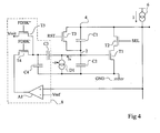
- figure 4 schematically represents a CMOS light sensing
cell according to an alternative embodiment of the invention.
-
-
Same reference numbers correspond to same elements in
the different figures. For clarity's sake, only the elements
that are useful to the understanding of the invention have been
illustrated.
-
Figure 2 schematically represents a CMOS light sensing
cell according to an embodiment of the invention, comprising a
sensor D1, capacitors C1 and C2, and CMOS transistors T1, T2 and
T3, connected as in figure 1.
-
According to the invention, the sensing cell further
comprises a feedback block 8 comprised of an operational
amplifier A1, capacitors C3 and C4 and a MOS transistor T4 of N-channel
type. The non-inverting and inverting input of the
operational amplifier A1 are respectively connected to the
output node 4 and to a reference voltage Vref that will be
described later. The output of the operational amplifier A1 is
connected to the source of transistor T4. The gate of transistor
T4 is connected to a non-illustrated control block supplying a
feedback control signal FDBK. The drain of transistor T4 is
connected to the sensing node 2 through the capacitor C3. The
drain of transistor T4 is connected to the ground through the
capacitor C4.
-
The operation of a light sensing cell according to the
invention is as follows. As in a typical light sensing cell, the
transistor T2 is first closed to select the cell, then the
transistor T3 is closed for a given reset time to reset the
cell. According to the invention, the signal FDBK is activated
to close transistor T4 when the transistor T3 is closed
(preferably, transistors T3 and T4 are closed simultaneously).
-
After a transitory state following the closing of T3
and T4, the cell stabilizes in a stable state where capacitor C1
is discharged and capacitor C2 is charged to a voltage Vrst. The
non-inverting input of the operational amplifier A1 then
receives the voltage Vrst of node 4, and amplifier A1 supplies a
given feedback voltage Vfbk that depends on Vrst-Vref and on the
amplifying factor of A1. Capacitors C4 and C3 are then charged
through transistor T3 respectively to the voltage Vfbk, and to a
voltage Vrst-Vfbk. The voltage Vfbk can be set to a desired
value by an appropriate value of the reference voltage Vref.
-
According to the invention, the signal FDBK is kept
activated so that transistor T4 remains closed a predetermined
time after transistor T3 has been opened. Hence, when capacitor
C1 is charged with a random parasitic voltage at the opening of
transistor T3, the output of amplifier A1 supplies a voltage
equal to the sum of the feedback voltage Vfbk and of a variation
proportional to the parasitic voltage on node 4. Since the
capacitor C3 cannot charge any more through the transistor T3,
the cell is after the opening of transistor T3 in a transitory
state where the variation of the voltage of the output of
amplifier A1 is transmitted through capacitor C3 to node 2,
which causes the conductivity of transistor T1 to increase,
whereby discharging capacitor C1 and bringing the voltage of
node 4 back to Vrst which is then free of the unwanted noise
voltage.
-
One skilled in the art will understand that the
feedback block 8 may first over-discharge the capacitor C1, and
that the feedback loop may bring the voltage of node 4 to Vrst
after a few damped oscillations. The transistor T4 is opened
after a predetermined time that is chosen so as to let the
feedback loop substantially discharge the capacitor C1, and so
as to be very short compared to the integration time. For
example, the transistor T4 may be left closed for 5 µs after the
opening of transistor T3, while a typical integration time is of
about 10 ms. After the signal FDBK is inactivated, the capacitor
C1 charges classically as a function of the sensing current. The
reading of the output voltage after the integration time in a
light sensing cell according to the invention is as in a typical
light sensing cell.
-
The transistor T4 being of the same type as the
transistor T3, a random noise current flows through the
transistor T4, and the capacitor C4 remains charged with a
random parasitic voltage ΔV when the transistor T4 is opened.
According to the invention, the value of capacitor C4 is chosen
bigger than capacitor C2, so as to minimize the noise voltage
ΔV. In addition, the capacitor C3 is chosen smaller than the
capacitor C1, so that a reduced noise voltage δV = ΔV.C3/C1 is
transmitted to the node 4 when the transistor T4 is opened.
-
A sensing cell according to the invention therefore
provides for a substantially reduced parasitic voltage on its
output node 4 after it has been reset, whereby improving the
performance of the cell in the dark. As an example, for
capacitors C1 and C2 having respective values of 2 and 6 fF,
capacitor C3 may have a value of 0.5 fF and capacitor C4 a value
of 10 fF, to reduce the maximum kTC noise to 200 µV.
-
The operational amplifier A1, the transistor T4 and
the capacitors C3, C4 are typical CMOS elements and a sensing
cell according to the invention can be manufactured using a
typical CMOS process.
-
Figure 3 schematically represents one of a plurality
of columns of an integrated CMOS light sensing array according
to an embodiment of the invention. The column is comprised of a
number n of light sensing cells SC1 to SCn according to the
invention. Each light sensing cell has substantially the same
structure as the cell illustrated in figure 2, with the
exception that the amplifier A1 is shared by the feedback block
of each cell of the column. One single current source 6 is
connected to the output node of all the cells of the column.
Each cell SC1 to SCn of the column is provided with an
individual selection signal SEL1 to SELn, an individual reset
signal RST1 to RSTn, and an individual feedback control signal
FDBK1 to FDBKn.
-
This allows for reducing the size of each cell, and
therefore the size and cost of the light sensing array.
-
The operation of the light sensing cells according to
this second embodiment is as for the light sensing cell
described in relation with figure 1.
-
Figure 4 schematically represents a CMOS light sensing
cell according to an alternative embodiment of the invention,
comprising as the cell illustrated in figure 2 a sensor D1,
capacitors C1 and C2, CMOS transistors T1, T2 and T3 and a
feedback block 8. According to this alternative embodiment, the
feedback block 8 comprises an additional transistor T5. The
amplifier A1, the capacitors C3, C4 and the transistor T4 are
connected as in figure 2, although the transistor T4 does not
receive the feedback control signal FDBK but a signal FDBK'. The
transistor T5 is a MOS transistor of N-channel type that has a
source connected to a fixed voltage Vinit and a drain connected
to the drain of transistor T4. The gate of transistor T4
receives a feedback control signal FDBK".
-
The operation of a light sensing cell according to
this embodiment is as follows. As in the light sensing cell of
figure 2, the transistor T2 is first closed to select the cell,
then the transistor T3 is closed for a given reset time to reset
the cell. According to the invention, the signals FDBK' and
FDBK" are initially inactivated so as to open transistors T4 and
T5. The signal FDBK" is then activated to close transistor T5
while the transistor T3 is still closed and at least until the
transistor T3 is opened. When the signal FDBK" is inactivated,
the signal FDBK' is activated for a predetermined duration. The
sum of the duration of the active states of the signals FDBK'
and FDBK" is substantially equal to the duration of the signal
FDBK previously described in relation with figure 2.
-
After a transitory state following the closing of T3
and T5, the cell stabilizes in a stable state where capacitor C1
is discharged, capacitor C2 is charged to Vrst, capacitor C4 is
charged to Vinit and capacitor C3 is charged to Vrst-Vinit.
-
As previously described, amplifier A1 then supplies a
given feedback voltage Vfbk that depends on Vrst-Vref and on the
amplifying factor of A1. When the transistor T5 is opened and
transistor T4 is closed, the feedback voltage Vfbk is supplied
to the capacitor C3. Since the capacitor C3 is still charged to
Vrst-Vinit, the voltage of node 2 is then equal to Vrst-Vinit+Vfbk.
The cell then enters a transitory state during which
the capacitor C1 charges (or discharges) to a fixed value for
which the node 4 has a voltage such that the feedback loop
brings the voltage of node 2 back to Vrst, at which time the
cell is stabilized and the signal FDBK' can be inactivated. It
can be shown that the final voltage of node 4 is set by Vinit,
Vref and by the characteristics of the feedback loop, whatever
the charge of capacitor C1 was at the opening of transistor T3
and whatever noise voltage was stored in capacitor C1. After the
signal FDBK' is inactivated, the capacitor C1 charges
classically as a function of the sensing current. The voltage of
node 4 when the signal FDBK' is inactivated being a set voltage,
non-illustrating offset means allow to correct the voltage
measured at node 4 at the end of the integration time.
-
One skilled in the art will notice that the above
embodiment of the invention is particularly useful to suppress
the components of the noise voltage that are slower than the
feedback loop.
-
Of course, the present invention is likely to incur
various alterations, modifications, and improvements which will
readily occur to those skilled in the art. In particular, the
operational amplifier of the feedback block may be formed in any
known manner.
-
Also, it has been described above that the transistor
T2 remains closed from the reset of the light sensing cell and
during its integration time. However, the transistor T2 can be
opened after the opening of the transistor T4, just to be closed
only a short while at the end of the integration time, in order
to allow for the reading of the output voltage of the sensing
cell.
-
The transistor T2 can also be suppressed in light
sensing cells that do not share a supply current source, such as
the cells of a single row array for a scanner device. The
invention has been described in relation with N-channel type MOS
transistors, but one skilled in the art will without difficulty
adapt the invention to P-channel MOS transistors, or to other
transistors having a similar operation.
-
Such alterations, modifications, and improvements are
intended to be part of this disclosure, and are intended to be
within the spirit and the scope of the present invention.
Accordingly, the foregoing description is by way of example only
and is not intended to be limiting. The present invention is
limited only as defined in the following claims and the
equivalents thereto.