EP1507410A1 - Reprogrammable control signal generator for video signals - Google Patents

Reprogrammable control signal generator for video signals Download PDF

Info

Publication number
EP1507410A1
EP1507410A1 EP04017521A EP04017521A EP1507410A1 EP 1507410 A1 EP1507410 A1 EP 1507410A1 EP 04017521 A EP04017521 A EP 04017521A EP 04017521 A EP04017521 A EP 04017521A EP 1507410 A1 EP1507410 A1 EP 1507410A1
Authority
EP
European Patent Office
Prior art keywords
video
microsequencers
control signal
timing generator
flags
Prior art date
Legal status (The legal status is an assumption and is not a legal conclusion. Google has not performed a legal analysis and makes no representation as to the accuracy of the status listed.)
Withdrawn
Application number
EP04017521A
Other languages
German (de)
French (fr)
Inventor
Brad Grossman
Aleksandr Movshovich
Current Assignee (The listed assignees may be inaccurate. Google has not performed a legal analysis and makes no representation or warranty as to the accuracy of the list.)
Avago Technologies International Sales Pte Ltd
Original Assignee
Broadcom Corp
Priority date (The priority date is an assumption and is not a legal conclusion. Google has not performed a legal analysis and makes no representation as to the accuracy of the date listed.)
Filing date
Publication date
Application filed by Broadcom Corp filed Critical Broadcom Corp
Publication of EP1507410A1 publication Critical patent/EP1507410A1/en
Withdrawn legal-status Critical Current

Links

Images

Classifications

    • GPHYSICS
    • G06COMPUTING; CALCULATING OR COUNTING
    • G06FELECTRIC DIGITAL DATA PROCESSING
    • G06F9/00Arrangements for program control, e.g. control units
    • G06F9/06Arrangements for program control, e.g. control units using stored programs, i.e. using an internal store of processing equipment to receive or retain programs
    • G06F9/30Arrangements for executing machine instructions, e.g. instruction decode
    • G06F9/30145Instruction analysis, e.g. decoding, instruction word fields
    • HELECTRICITY
    • H04ELECTRIC COMMUNICATION TECHNIQUE
    • H04NPICTORIAL COMMUNICATION, e.g. TELEVISION
    • H04N21/00Selective content distribution, e.g. interactive television or video on demand [VOD]
    • H04N21/40Client devices specifically adapted for the reception of or interaction with content, e.g. set-top-box [STB]; Operations thereof
    • H04N21/41Structure of client; Structure of client peripherals
    • H04N21/426Internal components of the client ; Characteristics thereof
    • H04N21/42607Internal components of the client ; Characteristics thereof for processing the incoming bitstream
    • H04N21/4263Internal components of the client ; Characteristics thereof for processing the incoming bitstream involving specific tuning arrangements, e.g. two tuners
    • HELECTRICITY
    • H04ELECTRIC COMMUNICATION TECHNIQUE
    • H04NPICTORIAL COMMUNICATION, e.g. TELEVISION
    • H04N5/00Details of television systems
    • H04N5/44Receiver circuitry for the reception of television signals according to analogue transmission standards
    • H04N5/46Receiver circuitry for the reception of television signals according to analogue transmission standards for receiving on more than one standard at will
    • HELECTRICITY
    • H04ELECTRIC COMMUNICATION TECHNIQUE
    • H04NPICTORIAL COMMUNICATION, e.g. TELEVISION
    • H04N5/00Details of television systems
    • H04N5/76Television signal recording
    • H04N5/91Television signal processing therefor
    • H04N5/913Television signal processing therefor for scrambling ; for copy protection
    • H04N2005/91357Television signal processing therefor for scrambling ; for copy protection by modifying the video signal
    • H04N2005/91364Television signal processing therefor for scrambling ; for copy protection by modifying the video signal the video signal being scrambled
    • HELECTRICITY
    • H04ELECTRIC COMMUNICATION TECHNIQUE
    • H04NPICTORIAL COMMUNICATION, e.g. TELEVISION
    • H04N7/00Television systems
    • H04N7/025Systems for the transmission of digital non-picture data, e.g. of text during the active part of a television frame
    • H04N7/035Circuits for the digital non-picture data signal, e.g. for slicing of the data signal, for regeneration of the data-clock signal, for error detection or correction of the data signal

Abstract

Systems and methods for generation of time-dependent control signals for video signals are provided. A system is provided that includes a set of microsequencers, a programmable combinational logic (PCL) module, shared memory, an arbiter for sharing of memory by the microsequencers, stacks containing registers for microsequencer control, and a control interface. The system can efficiently provide control signals for video signals, implement the MACROVISION copy protection process, and provide other value added features. The method includes accessing programs from shared memory, such that a set of microsequencers can generate flags. These flags are then processed to generate one or more control signals used to support the outputting of video signals including those requiring MACROVISION copy protection.

Description

BACKGROUND OF THE INVENTION Field of Invention
The present invention relates to video processing, and more particularly to the generation of time-dependent control signals for video signals.
Background
Television systems have become increasingly complex as consumers continue to demand greater functionality and performance from television sets. Furthermore, the geographic diversity and business interests of manufacturers and service providers within the television and recording industries has lead to a plethora of analog and digital video formats. For example, analog video signal formats include National TV System Committee (NTSC), Phase Alternation Line Rate (PAL), and Sequential Couleur Avec Memoire (SECAM) television signals. Example digital video signal formats include ITU-R-656 and Digital Video Interface (DVI). Moreover, video processing devices, such as a televisions or cable set-top boxes, must be able to insert control signals within video signals as they are being processed for display. Such control signals are needed to support outputting video signals in different formats and to implement a variety of value added features including, for example, copy protection features, such as those contained within MACROVISION copy protection process standards. MACROVISION is a trademark of Macrovision Corporation.
MACROVISION copy protection technologies are designed to allow content owners to protect their videocassettes, digital Pay-Per-View (PPV) programs and digital video discs (DVD) from unauthorized recording on VCRs. In the context of PPV, MACROVISION copy protection allows consumers to view, but not record, programs that are distributed via digital set-top box decoders. To apply copy protection to a specific program, the direct broadcast satellite (DBS) operator or cable system operator transmits a software command from the uplink center or headend to its set-top decoders. An integrated circuit inside the decoder receives the command and adds the copy protection waveform to the video destined for the TV. The copy-protected signal is transparent on original program viewing, but causes copies made on the majority of VCRs to degrade to the extent that they no longer have entertainment value. MACROVISION's PPV copy protection technology degrades unauthorized copies on approximately 95 percent of the TV and VCR combinations in the market today. Virtually all digital set-tops in North America have copy protection capability, as do the majority of digital set-top boxes in international markets.
The MACROVISION copy protection process requires that integrated circuitry within a video processing device dynamically adjust to copy protection information transmitted with a video stream. In addition, the MACROVISION copy protection process is an evolving one in which the formats used periodically change. For example, the current MACROVISION copy protection process has been revised and updated several times, and is currently on Revision 7.1.S1. Implementation of the MACROVISION copy protection process has been previously implemented in hardware because of the need to quickly process MACROVISION input signals and generate control signals to adjust an output video signal. As a result, when revisions to the standard are made, updating deployed video processing devices that have used hardware to implement the MACROVISION standard is difficult.
What is needed are systems and methods for generation of time-dependent control signals that can efficiently provide control for video signals, implement the MACROVISION copy protection process, and provide other value added features.
SUMMARY OF THE INVENTION
The present invention provides systems and methods for generation of time-dependent control signals for video signals. A system is provided that includes a set of microsequencers, a programmable combinational logic (PCL) module, shared memory, an arbiter for sharing of memory by the microsequencers, stacks containing registers for microsequencer control, and a control interface. The system can efficiently provide control signals for video signals, implement the MACROVISION copy protection process, and provide other value added features. The method includes accessing programs from shared memory, such that a set of microsequencers can generate flags. These flags are then processed to generate one or more control signals used to support the outputting of video signals including those requiring MACROVISION copy protection.
The generation of control signals is software controlled, thereby allowing the system to be reconfigured in real time, and permitting simple modification to reflect changes in the MACROVISION copy protection process and other value added features for video signals. The invention provides an efficient way to flexibly produce time-dependent control signals for video signals.
According to an aspect of the invention, a timing generator for use within a video processing device comprises:
  • a random access memory;
  • a plurality of microsequencers coupled to said random access memory that produce flags based on programs stored in said random access memory; and
  • a programmable combinational logic module, coupled to said plurality of microsequencers that generates control signals based on the flags produced by
  • said plurality of microsequencers.
  • Advantageously, the timing generator further comprises:
    • a plurality of shift registers, coupled to said plurality of microsequencers that
    • provide operating parameters to said plurality of microsequencers.
    Advantageously, the timing generator further comprises:
    • a means for downloading software changes to said timing generator while said timing generator is processing a video signal without substantial interference to a
    • video signal being processed.
    Advantageously, the timing generator further comprises:
    • an instruction set that enables said plurality of microsequencers to share said
    • random access memory.
    Advantageously, said plurality of microsequencers includes between two and ten microsequencers.
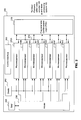
    Advantageously, said plurality of microsequencers includes seven microsequencers.
    Advantageously, said programmable combinational logic produces control signals that support a copy protection process.
    Advantageously, the copy protection process is a MACROVISION copy protection process.
    Advantageously, said video processing device is a television.
    Advantageously, said video processing device is a cable set-top box.
    According to an aspect of the invention, a video processing system comprises:
    • a video input interface;
    • a video decoder coupled to said video input interface;
    • a video and graphics processor coupled to said video decoder;
    • a video encoder coupled to said video and graphics processor; and
    • a video output interface coupled to said video encoder,
       wherein said video encoder includes a timing generator.
    Advantageously, said timing generator contains software for implementing a MACROVISION copy protection process.
    Advantageously, said video processing system has been implemented on a single integrated circuit.
    According to an aspect of the invention, a method for generating a time-dependent control signal for video signals comprises the steps of:
    • (a) storing a plurality of programs within a random access memory;
    • (b) accessing a plurality of programs stored within the random access memory;
    • (c) executing a set of programs from said plurality of programs by a plurality of microsequencers to generate a set of flags;
    • (d) generating a control signal based on the set of flags through application of programmable controlled logic; and
    • (e) outputting said control signal.
      Advantageously, the step of accessing includes arbitrating the access to the random access memory by the plurality of microsequencers.
      Advantageously, the step of executing is completed in parallel by a plurality of microsequencers.
      Advantageously, the control signal is a control signal used to implement a MACROVISION copy protection process.
      Advantageously, the control signal is a horizontal sync control signal.
      Advantageously, the control signal is an external horizontal sync control signal.
      Advantageously, the control signal is an external vertical sync control signal.
      Advantageously, the control signal is a vertical blanking active control signal.
      Advantageously, the control signal is a color burst control signal.
      Advantageously, the control signal is a U Flip control signal to generate MACROVISION color stripes.
      Advantageously, the control signal is a V Flip control signal to generate MACROVISION color stripes.
      Advantageously, the control signal is a vertical sync control signal.
      Advantageously, the control signal is a vertical blank control signal.
    Further embodiments, features, and advantages of the present inventions, as well as the structure and operation of the various embodiments of the present invention, are described below.
    BRIEF DESCRIPTION OF THE FIGURES
    The invention is described with reference to the accompanying drawings. In the drawings, like reference numbers indicate identical or functionally similar elements. The drawing in which an element first appears is indicated by the left-most digit in the corresponding reference number.
    FIG. 1 is a diagram of a video processing system, according to an embodiment of the invention.
    FIG. 2 is a diagram of a timing generator, according to an embodiment of the present invention.
    FIG. 3 is a diagram a timing generator designed for use with MACROVISION copy protection processes, according to an embodiment of the invention.
    FIG. 4 is a diagram of programmable combinational logic, according to an embodiment of the invention.
    FIG. 5 is a flowchart of a method to generate a time-dependent control signal for video signals, according to an embodiment of the invention.
    DETAILED DESCRIPTION OF THE INVENTION
    While the present invention is described herein with reference to illustrative embodiments for particular applications, it should be understood that the invention is not limited thereto. Those skilled in the art with access to the teachings provided herein will recognize additional modifications, applications, and embodiments within the scope thereof and additional fields in which the present invention would be of significant utility.
    FIG. 1 provides a diagram of an example video processing system 100, according to an embodiment of the invention. A video processing system, such as video processing system 100, receives video input signals and manipulates the stream to properly format an output video stream. A video processing system, such as video processing system 100, can also integrate graphics and text (e.g., teletext) into the video stream and output a reformatted video stream. Finally, video processing system 100 can be used to implement value added features, such as copy protection features. Video processing system 100 will typically be located within a video processing device, such as a television or cable set-top box.
    Video processing system 100 includes video input interface 110, video decoder 120, video and graphics processor 130, video encoder 140 and video output interface 150. Video input interface 110 receives a video input signal that can be either digital or analog. Video decoder 120 can support decoding and encoding of both analog and video input signals, and is coupled to the output of video input interface 110. Video decoder 120 can support high quality decoding of a standard definition analog composite video broadcasting signal (CVBS) and S-Video signals, for example. Similarly, video decoder 120 can decode digital video signals that comply with the International Telecommunications Union (ITU) standard ITU-R-656 at varying resolutions including 525i, 625i, and 240p.
    Video and graphics processor 130 includes a variety of functions for processing video and graphics, including integrating video and graphics, and is coupled to the output of video decoder 120. In particular, video and graphics processor 130 can include MPEG graphics and video feeders, video scalers, capture blocks, and video compositors for combining video and graphics, and the like.
    Video encoder 140 can support both standard and high definition video signals, and is coupled to the output of video and graphics processor 130. For example, video encoder 140 can support a variety of analog video standards (e.g., NTSC, PAL, SECAM, 480i, 480p, 720p, and 1080i), as well as digital video standards (e.g., ITU-R-656 and support for digital video interface (DVI) encoding). Video encoder 140 performs a variety of functions to encode an output video stream. In particular, video encoder 140 includes a color space converter to convert the input color to any component-color format. In addition, the video encoder 140 contains filters to determine a video channel's frequency response as required by the various video standards. Video encoder 140 can occasionally stall video signal processing to insert blanking signals into the video stream. For analog formats, these blanking signals can be quite elaborate - merging syncs, backporchs, pseudo syncs, automatic gain control (AGC) bursts, color burst envelops, and vertical blanking intervals. In addition, video encoder 140 can manipulate a video signal to support copy protection features, such as those of MACROVISION.
    Video output interface 150 can include a set of analog and digital output interfaces to support a multitude of video standards, and is coupled to the output of video encoder 140. Video output interface 150 can be coupled to a video processing device, such as a television, a monitor, or a cable set top box to display a video signal or for further processing. Video processing system 100 can be implemented on a single integrated circuit or on multiple integrated circuits.
    FIG. 2 provides a diagram of timing generator 200, according to an embodiment of the present invention. A timing generator, such as timing generator 200, can exist within video encoder 140 to provide control signals to support output video signals and copy protection standards, such as the MACROVISION copy protection process. In particular, timing generator 200 can produce a variety of time-dependent control signals for various video formats, both digital and analog. For example, these can include horizontal and vertical synchronization signals and active video signals. Additional control signals for composite formats involve timing of the sub-carrier bursts (color bursts and bottles). Timing generator 200 can also generate control signals required for MACROVISION encoding, such as color stripe, AGC and pseudo sync pulses, reduced sync, and back porch pulses. Timing generator 200 specifies when these control signals should occur. Other portions of video encoder 140 or video processing system 100 actually insert or combine these signals.
    Example control signals that can be generated by timing generator 200 are as follows:
    • Horizontal Sync Control Signal. This signal includes equalization and serration pulses, as well as pseudo-syncs for MACROVISION.
    • External Horizontal Control Signal. This signal is generally the same as the Horizontal Sync Control Signal, except that it generates a standard horizontal sync on every line and nothing else.
    • External Vertical Sync Control Signal. This signal is similar to a vertical active signal, but allows for differences in digital and analog formats.
    • Vertical Blanking Active Control Signal. This signal is used during blanking a line or if the vertical active signal analog line length is different than required by a vertical blanking interval encoder.
    • Color Burst Control Signal. This signal generates color burst timing. This control signal must also be on during MACROVISION color stripe.
    • U Flip Control Signal. This signal is used to generate MACROVISION color stripes. The signal inverts the phase of the U component of the color burst. This signal is not used to change the phase of the color burst for PAL/NSTC, which is done by another mechanism.
    • V Flip Control Signal. This signal is used to generate MACROVISION color stripes. The signal inverts the phase of the V component of the color burst. This signal is not used to change the phase of the color burst for PAL/NSTC, which is done by another mechanism.
    • V Sync Control Signal. This signal is used to support vertical sync.
    • V Blank Control Signal. This signal is used to support vertical blank.
    • Horizontal Active Video Control Signal. This signal supports the horizontal portion of active video. The signal denotes which areas of a horizontal line have video information within them.
    • Vertical Active Video Control Signal. This signal supports the vertical portion of active video. The signal denotes which vertical lines have video information on them.
    • Bottles Control Signal. This signal supports bottle signals needed for SECAM.
    • Odd/Even Control Signal. This signal denotes which field is currently being encoded. The falling edge of this signal is used as a new frame signal.
    • New Line Control Signal. This signal is used to mark a new line and is used in the determination of which phase to give to the current line.
    • AGC Control Signal. This signal is used to generate AGC pulses in an AGC multiplexer.
    • Back Porch Control Signal. This signal is used to generate the back porch signal to the AGC multiplexer.
    Timing generator 200 includes a set of microsequencers, such as microsequencers 205A through 205G; programmable combinational logic (PCL) module 210; random access memory 220; arbiter 230; stacks 240; and control interface 250. In one embodiment, timing generator 200 can be implemented on a single integrated circuit.
    Each microsequencer 205 is a microcontroller operating independently of each other, but in a coordinated manner. When synchronized, microsequencers 205A through 205G generate proper timing signals indirectly by outputting flags that are combined in PCL module 210 to produce control signals. Each microsequencer includes a counter (not shown) to sustain timing and generate a flag or set of flags for a specified amount of time. Microsequencers 205A through 205G are fully configurable and capable of supporting all current video standards. The differences between microsequencers 205A through 205G are (1) the number of flags maintained, (2) how the flags are fed as events to other microsequencers for coordinated operation, (3) how the flags are provided to PCL module 210 and (4) whether a particular microsequencer can be restarted. As is explained with reference to FIG. 3, microsequencers 205A through 205G can be partitioned in a variety of ways, such that tasks are distributed efficiently across the microsequencers. The outputs of microsequencers are coupled to PCL module 210 and to each other along a bus structure 270 that allows operation of the microsequencers to be coordinated.
    PCL module 210 contains logic that allows a system programmer to select which combination of microsequencer flags generates control signals to be forwarded to other elements of a video encoder, such as video encoder 140. Specific examples related to control signals used for MACROVISION are discussed below. PCL module 210 has its output coupled to a variety of other elements within a video encoder that use the control signals to manipulate the video signals being processed.
    Random access memory (RAM) 220 contains programs used by the microsequencers. The programs for all microsequencers 205A through 205G exist within RAM 220 to increase timing generator 200 flexibility and reduce gates needed in the implementation of timing generator 200. That is, RAM 220 is a shared resource among all microsequencers 205A through 205G. Within RAM 220 there are multiple programs running concurrently. The programs contained within RAM 220 are based on a microsequencer instruction set. Each command within the instruction set has four fields. These fields include a three bit opcode field that determines the command type and a one bit return flag field that determines whether to return from a subroutine. In addition, each command contains an eight bit field, referred to as the flag field, which is used to set flags within a microsequencer, select addresses, or to select which microsequencer to restart. Another twelve bit field, referred to as the count/register field, specifies a count or a register stack to select from stacks 240. The count parameter specifies how long a certain flag should be output by a microsequencer.
    Arbiter 230 fetches instructions from RAM 230 for each microsequencer 205 in the set of microsequencers. Arbiter 230 provides arbitration of requests from microsequencers 205A through 205G to access memory resources within RAM 230
    Stacks 240 comprises set of eight 16 bit shift registers. The registers are loaded with data that is accessed by the microsequencers based on the programs being run within RAM 220.
    Control interface 250 provides a means for a host or other components to provide administrative instructions to timing generator 200. For example, control interface 250 can be used to receive an indication that MACROVISION copy processing process should begin. Upon receipt of such instruction, the proper information can be loaded into registers and the appropriate programs run from RAM 220.
    The number of microsequencers and the specific function that each microsequencer performs (i.e., what flags will the microsequencer produce) is flexible. In alternate embodiments, any number of microsequencers can be used. However, typically between two and ten microsequencers will be used. In addition to the number of microsequencers, the specific function performed by each of the microsequencers can be varied based on the primary functions that timing generator 200 will perform.
    FIG. 3 is a diagram of an example timing generator 300 that has been designed to support MACROVISION copy protection process, according to an embodiment of the invention. Timing generator 300 is the same as timing generator 200 except that the design of the microsequencers, programs, and programmable combinational logic has been optimized to support MACROVISION copy protection process. As in the case of timing generator 200, timing generator 300 includes a set of microsequencers, such as microsequencers 305A through 305G; programmable combinational logic (PCL) module 310; random access memory 320; arbiter 330; stacks 340; and control interface 350.
    The components of timing generator 300 are similar to those of timing generator 200, except that each of microsequencers 350A through 350G have been designed to perform specific operations in support of MACROVISION copy protection process. In particular, microsequencer 350A is configured to provide flags supporting the horizontal standard for MACROVISION. Microsequencer 350B is configured to support the vertical standard. Microsequencer 350C is configured to support the horizontal AGC/PS standard. Microsequencer 350D is configured to support the vertical AGC/PS standard. Microsequencer 350E is configured to support the back porch signal requirement. Microsequencer 350F is configured to support the vertical color stripe. And, microsequencer 350G is configured to support the horizontal color stripe. Configuring the microseqencers for a particular function entails providing programs to produce specific sets of flags associated with the function corresponding to the particular microsequencer. In addition, logic within programmable combinational logic module 310 is configured to expect certain flags from each of the microsequencer and to produce the appropriate control signal based on those flags. Timing Generator 300 provides one embodiment on how to implement the MACROVISION copy protection process, and is not intended to limit the scope of the invention. Based on the teachings herein, individuals skilled in the relevant arts will be able to discern additional embodiments.
    FIG. 4 provides a diagram of programmable combinational logic, according to an embodiment of the invention. FIG. 4 provides explicit notation showing how flags that are output from microsequencers can be used to generate control signals by application of logic within a programmable combinational logic module, such as PCL module 310. The logic diagram includes multiplexers 405A through 405E, AND gates 410A through 410E, OR gate 420 and multiplexers 425A through 425D. The programmable logic within a PCL module is configured to mimic the operation of these types of devices to produce the desired control signal. In the example provided the principal flag inputs are from microsequencer 350A (horizontal standard) and microsequencer 350B (vertical standard). In addition, various inputs from other microsequencers would be input into multiplexers 425A through 425D. For ease of illustration, the specific inputs to multiplexers 425A through 425D will not be discussed. A discussion relative to the inputs of microsequencer 350A and 350B provides sufficient insight to individuals skilled in the relevant arts to understand the construction of the programmable combinational logic.
    Microsequencer 350A produces three flags: Hsync Hequalization, and Hserration. Microsequencer 350B also produces three flags: Vsync, Vequal only, and Vnot equalization. Each of multiplexers 405A through 405E receives as inputs a low signal, a high signal, an output from multiplexer 425A, an output from multiplexer 425B, the Vnot equalization flag, the Vequal flag and the Vsync flag.
    In this particular embodiment, multiplexer 405A has a register controlled input, such that only the Vnot equalization input will be permitted through. The register controlled input allows modification of the programmable combinational logic in a PCL module, such that the logic can be easily adapted for changes to the MACROVISION standard or for other purposes. In this case, when Vnot equalization is a 1, multiplexer 405A will transmit a 1, and when Vnot equalization is a 0, multiplexer 405A will transmit a 0. The output of multiplexer 405A is input into AND gate 410A. The other input of AND gate 410A is the Hsync flag from microsequencer 350A. Therefore, when both Hsync and Vnot equalization are a 1, AND gate 410A will output a 1. In all other cases, AND gate 410A will output a 0. The output of AND gate 410A is input into OR gate 420 to generate the Sync control signal. Thus, if both Hsync and V not equalization are both a 1, the Sync control signal will be a 1. In all other cases, whether the Sync control signal is a 1 will be controlled by the other AND gates that are coupled to OR gate 420.
    Multiplexer 405B has a register controlled input, such that only the Vequal only input will be permitted through. In this case, when Vequal only is a 1, multiplexer 405B will transmit a 1, and when Vequal only is a 0, multiplexer 405B will transmit a 0. The output of multiplexer 405B is input into AND gate 410B. The other input of AND gate 410B is the Hequalization flag from microsequencer 350A. Therefore, when both Hequalization and Vequal only are a 1, AND gate 410B will output a 1. In all other cases, AND gate 410B will output a 0. The output of AND gate 410B is input into OR gate 420 to generate the Sync control signal. Thus, if both Hequalizationand Vequal only are both a 1, the Sync control signal will be a 1. In all other cases, whether the Sync control signal is a 1 will be controlled by the other AND gates that are coupled to OR gate 420.
    Multiplexer 405C has a register controlled input, such that only the Vsync input will be permitted through. In this case, when Vsync is a 1, multiplexer 405C will transmit a 1, and when Vsync is a 0, multiplexer 405C will transmit a 0. The output of multiplexer 405C is input into AND gate 410C. The other input of AND gate 410C is the Hserration flag from microsequencer 350A. Therefore, when both Hserration and Vsync are a 1, AND gate 410C will output a 1. In all other cases, AND gate 414C will output a 0. The output of AND gate 410C is input into OR gate 420 to generate the Sync control signal. Thus, if both Hserration and Vsync are both a 1, the Sync control signal will be a 1. In all other cases, whether the Sync control signal is a 1 will be controlled by the other AND gates that are coupled to OR gate 420.
    Multiplexer 405D has a register controlled input, such that only the input received from the output of multiplexer 425A will be permitted through. In this case, when the output of multiplexer 425A is a 1, multiplexer 405D will transmit a 1, and when the output of multiplexer 425A is a 0, multiplexer 405D will transmit a 0. The output of multiplexer 405D is input into AND gate 410D. The other input of AND gate 410D is the output of multiplexer 425C. Therefore, when both outputs from multiplexers 425A and 425C are a 1, AND gate 410D will output a 1. In all other cases, AND gate 410D will output a 0. The output of AND gate 410D is input into OR gate 420 to generate the Sync control signal. Thus, if both outputs from multiplexers 425A and 425C are 1, the Sync control signal will be a 1. In all other cases, whether the Sync control signal is a 1 will be controlled by the other AND gates that are coupled to OR gate 420. The inputs into multiplexers 425A and 425C will be other flags from microsequencers, subject to the desired functionality.
    Multiplexer 405E has a register controlled input, such that only the input received from the output of multiplexer 425B will be permitted through. In this case, when the output of multiplexer 425B is a 1, multiplexer 405D will transmit a 1, and when the output of multiplexer 425B is a 0, multiplexer 405E will transmit a 0. The output of multiplexer 405E is input into AND gate 410E. The other input of AND gate 410E is the output of multiplexer 425D. Therefore, when both outputs from multiplexers 425B and 425D are a 1, AND gate 410E will output a 1. In all other cases, AND gate 410E will output a 0. The output of AND gate 410E is input into OR gate 420 to generate the Sync control signal. Thus, if both outputs from multiplexers 425B and 425D are 1, the Sync control signal will be a 1. In all other cases, whether the Sync control signal is a 1 will be controlled by the other AND gates that are coupled to OR gate 420. The inputs into multiplexers 425B and 425D will be other flags from microsequencers, subject to the desired functionality.
    Similar programmable combinational logic can be developed to implement each of the other control signals described above, as will be apparent to individuals skilled in the relevant arts based on the teachings herein.
    FIG. 5 is a flowchart of method 500 to generate a time-dependent control signal for video signals, according to an embodiment of the invention. Method 500 begins in step 505. In step 505, a set of flags is generated. In one embodiment, a set of flags can be generated by some or all of the microsequencers 205A through 205G executing programs that were accessed from RAM 220. In accessing programs from RAM, arbiter 230 can arbitrate access from the microsequencers, such that microsequencers can request programs simultaneously and arbiter 230 will arbitrate the access. For example, referring to FIG. 4, microsequencer 350A can generate flags Hsync, Hequalization and Hserration. Similarly, microsequencer 350B can generate flags Vsync, Vequal only and Vnot equalization.
    In step 510, a control signal is generated. For example, referring again to FIG. 4 the flags generated by microsequencer 350A and microsequencer 350B can be provided to PCL module 310 where the programmable combination logic described with reference to FIG. 4 can be applied to the flags to generate a Sync control signal, depending on the values of the flags.
    In step 515, the control signal is output. For example, a Sync, AGC or back porch control signal can be provided to a V/H blank generator located within video encoder 140 to instruct a V/H blank generator to insert a blank line.
    In step 520, a determination is made as to whether the control signal should continue to be output. For example, when generating a MACROVISION color stripe for a PAL signal, a color stripe replaces the color burst for two to five consecutive lines. Thus, the control signals must be output for a particular period of time to ensure that the color stripe is provided for the time is takes to output two to five lines. In this case, the programs running the microsequencers would contain counters to ensure that the appropriate flags were produced for the needed amount of time. If a determination is made that the control signal should end, method 500 proceeds to step 525. In step 525 the microsequencers are reset to stop producing the current flags, and a new program is loaded to begin producing the next set of flags necessary. Method 500 then proceeds back to step 505 to begin the process over with new programs loaded for the microsequencers.
    If a determination is made that the control signal should not end in step 520, method 500 proceeds to step 530. In step 530 a determination is made whether processing should be terminated. If a determination is made that processing should end, method 500 proceeds to step 535, and method 500 ends. If a determination is made that processing should not end, method 500 returns to step 510 to continue to generate the control signal.
    Conclusion
    While various embodiments of the present invention have been described above, it should be understood that they have been presented by way of example, and not limitation. It will be apparent to persons skilled in the relevant art that various changes in form and detail can be made therein without departing from the spirit and scope of the invention.
    The present invention has been described above with the aid of functional building blocks and method steps illustrating the performance of specified functions and relationships thereof. The boundaries of these functional building blocks and method steps have been arbitrarily defined herein for the convenience of the description. Alternate boundaries can be defined so long as the specified functions and relationships thereof are appropriately performed. Any such alternate boundaries are thus within the scope and spirit of the claimed invention. One skilled in the art will recognize that these functional building blocks can be implemented by discrete components, application specific integrated circuits, processors executing appropriate software and the like or any combination thereof. Thus, the breadth and scope of the present invention should not be limited by any of the above-described exemplary embodiments, but should be defined only in accordance with the following claims and their equivalents.

    Claims (10)

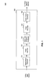
    1. A timing generator for use within a video processing device, comprising:
      a random access memory;
      a plurality of microsequencers coupled to said random access memory that produce flags based on programs stored in said random access memory; and
      a programmable combinational logic module, coupled to said plurality of microsequencers that generates control signals based on the flags produced by
         said plurality of microsequencers.
    2. The timing generator of claim 1, further comprising:
      a plurality of shift registers, coupled to said plurality of microsequencers that provide operating parameters to said plurality of microsequencers.
    3. The timing generator of claim 1 or 2, further comprising:
      a means for downloading software changes to said timing generator while said timing generator is processing a video signal without substantial interference to a video signal being processed.
    4. The timing generator of any of the preceding claims, further comprising:
      an instruction set that enables said plurality of microsequencers to share said random access memory.
    5. A video processing system, comprising:
      a video input interface;
      a video decoder coupled to said video input interface;
      a video and graphics processor coupled to said video decoder;
      a video encoder coupled to said video and graphics processor; and
      a video output interface coupled to said video encoder,
         wherein said video encoder includes a timing generator.
    6. A video processing system of claim 5, wherein said timing generator contains software for implementing a MACROVISION copy protection process.
    7. A video processing system of claim 5 or 6, wherein said video processing system has been implemented on a single integrated circuit.
    8. A method for generating a time-dependent control signal for video signals, comprising the steps of:
      (a) storing a plurality of programs within a random access memory;
      (b) accessing a plurality of programs stored within the random access memory;
      (c) executing a set of programs from said plurality of programs by a plurality of microsequencers to generate a set of flags;
      (d) generating a control signal based on the set of flags through application of programmable controlled logic; and
      (e) outputting said control signal.
    9. The method of claim 8, wherein the step of accessing includes arbitrating the access to the random access memory by the plurality of microsequencers.
    10. The method of claim 8 or 9, wherein the step of executing is completed in parallel by a plurality of microsequencers.
    EP04017521A 2003-08-14 2004-07-23 Reprogrammable control signal generator for video signals Withdrawn EP1507410A1 (en)

    Applications Claiming Priority (2)

    Application Number Priority Date Filing Date Title
    US640627 2003-08-14
    US10/640,627 US7555125B2 (en) 2003-08-14 2003-08-14 Systems and methods for generation of time-dependent control signals for video signals

    Publications (1)

    Publication Number Publication Date
    EP1507410A1 true EP1507410A1 (en) 2005-02-16

    Family

    ID=33565264

    Family Applications (1)

    Application Number Title Priority Date Filing Date
    EP04017521A Withdrawn EP1507410A1 (en) 2003-08-14 2004-07-23 Reprogrammable control signal generator for video signals

    Country Status (2)

    Country Link
    US (1) US7555125B2 (en)
    EP (1) EP1507410A1 (en)

    Families Citing this family (5)

    * Cited by examiner, † Cited by third party
    Publication number Priority date Publication date Assignee Title
    US7489362B2 (en) 2003-03-04 2009-02-10 Broadcom Corporation Television functionality on a chip
    US9289398B2 (en) 2006-03-30 2016-03-22 Ptc Therapeutics, Inc. Methods for the production of functional protein from DNA having a nonsense mutation and the treatment of disorders associated therewith
    US8457122B2 (en) * 2007-08-01 2013-06-04 Broadcom Corporation Multiport switch for cascaded ethernet AV device networking
    US8393008B2 (en) * 2008-05-21 2013-03-05 Microsoft Corporation Hardware-based output protection of multiple video streams
    US20090317057A1 (en) * 2008-06-24 2009-12-24 Hua Wu Apparatus and method for selectively outputting hd/sd signals as high definition video according to copy protection

    Citations (2)

    * Cited by examiner, † Cited by third party
    Publication number Priority date Publication date Assignee Title
    US6381747B1 (en) * 1996-04-01 2002-04-30 Macrovision Corp. Method for controlling copy protection in digital video networks
    EP1244007A2 (en) * 2001-03-21 2002-09-25 Broadcom Corporation Dynamic microcode patching

    Family Cites Families (3)

    * Cited by examiner, † Cited by third party
    Publication number Priority date Publication date Assignee Title
    US5694588A (en) * 1993-05-07 1997-12-02 Texas Instruments Incorporated Apparatus and method for synchronizing data transfers in a single instruction multiple data processor
    JP3449106B2 (en) * 1996-03-06 2003-09-22 ソニー株式会社 Video signal processing apparatus, video signal processing method, and video signal recording / reproducing apparatus
    US6826352B1 (en) * 2000-03-29 2004-11-30 Macrovision Corporation Dynamic video copy protection system

    Patent Citations (2)

    * Cited by examiner, † Cited by third party
    Publication number Priority date Publication date Assignee Title
    US6381747B1 (en) * 1996-04-01 2002-04-30 Macrovision Corp. Method for controlling copy protection in digital video networks
    EP1244007A2 (en) * 2001-03-21 2002-09-25 Broadcom Corporation Dynamic microcode patching

    Non-Patent Citations (2)

    * Cited by examiner, † Cited by third party
    Title
    CHAOUI J ET AL: "OMAP: Enabling Multimedia Applications in Third Generation (3G) Wireless Terminals", TEXAS INSTRUMENTS WHITE PAPER, XX, XX, 1 December 2000 (2000-12-01), pages 1 - 12, XP002314534 *
    KAINKA B: "MICROCONTROLLER. ÖDRIVEN UART", ELEKTOR ELECTRONICS, ELEKTOR ELECTRONICS, GB, vol. 19, no. 217, 1 December 1993 (1993-12-01), pages 80 - 83, XP000417219, ISSN: 0268-4519 *

    Also Published As

    Publication number Publication date
    US20050036764A1 (en) 2005-02-17
    US7555125B2 (en) 2009-06-30

    Similar Documents

    Publication Publication Date Title
    US6263396B1 (en) Programmable interrupt controller with interrupt set/reset register and dynamically alterable interrupt mask for a single interrupt processor
    US7061509B2 (en) Method and apparatus for keying of secondary video into primary video
    US7680279B2 (en) Image display system
    US8212928B2 (en) Method of and apparatus for maintaining smooth video transition between distinct applications
    CN100499762C (en) Method and apparatus for simultaneous recording and displaying two different video programs
    EP0840512A2 (en) Integrated audio/video circuitry
    KR101031472B1 (en) Method and apparatus to communicate graphics overlay information
    CN1245830C (en) Method and apparatus for simultaneous recording and displaying two different video programs
    EP1143718A2 (en) Method for synchronizing a HDTV format change with a corresponding format change of an on screen display
    US7835400B2 (en) Method for data packet substitution
    EP1154643B1 (en) A method and system for using a single osd pixmap across multiple video raster sizes by using multiple headers
    US6573946B1 (en) Synchronizing video streams with different pixel clock rates
    US7555125B2 (en) Systems and methods for generation of time-dependent control signals for video signals
    EP1328114A1 (en) Image resolution management in a receiver/decoder
    US20050041807A1 (en) Display apparatus having lock operation for external input and method of implementing lock operation
    US7071991B2 (en) Image decoding apparatus, semiconductor device, and image decoding method
    JP4753274B2 (en) Method and integrated circuit for single pin reset in mixed signal integrated circuits
    JP2001083951A (en) Method for forming and processing image, osd forming method, image forming system and osd memory
    Yamauchi et al. Single chip video processor for digital HDTV
    US20020075294A1 (en) Digital broadcast receiving device and digital broadcast receiving method
    KR100320458B1 (en) Apparatus for displaying osd of analog/digital tv receiver
    US7782399B2 (en) System and a method to avoid on-screen fluctuations due to input signal changes while in an OSD or graphic centric mode
    JPH089343A (en) Video signal converter
    JP2006165893A (en) Digital broadcasting receiving device and digital broadcasting reception control method
    KR0123767B1 (en) Television the inside pip on screen display embodiment circuit

    Legal Events

    Date Code Title Description
    PUAI Public reference made under article 153(3) epc to a published international application that has entered the european phase

    Free format text: ORIGINAL CODE: 0009012

    AK Designated contracting states

    Kind code of ref document: A1

    Designated state(s): AT BE BG CH CY CZ DE DK EE ES FI FR GB GR HU IE IT LI LU MC NL PL PT RO SE SI SK TR

    AX Request for extension of the european patent

    Extension state: AL HR LT LV MK

    17P Request for examination filed

    Effective date: 20050816

    AKX Designation fees paid

    Designated state(s): DE FR GB

    RAP1 Party data changed (applicant data changed or rights of an application transferred)

    Owner name: BROADCOM CORPORATION

    17Q First examination report despatched

    Effective date: 20110208

    STAA Information on the status of an ep patent application or granted ep patent

    Free format text: STATUS: EXAMINATION IS IN PROGRESS

    APBK Appeal reference recorded

    Free format text: ORIGINAL CODE: EPIDOSNREFNE

    APBN Date of receipt of notice of appeal recorded

    Free format text: ORIGINAL CODE: EPIDOSNNOA2E

    APBR Date of receipt of statement of grounds of appeal recorded

    Free format text: ORIGINAL CODE: EPIDOSNNOA3E

    APAF Appeal reference modified

    Free format text: ORIGINAL CODE: EPIDOSCREFNE

    RAP1 Party data changed (applicant data changed or rights of an application transferred)

    Owner name: AVAGO TECHNOLOGIES GENERAL IP (SINGAPORE) PTE. LTD

    RAP1 Party data changed (applicant data changed or rights of an application transferred)

    Owner name: AVAGO TECHNOLOGIES INTERNATIONAL SALES PTE. LIMITE

    RIC1 Information provided on ipc code assigned before grant

    Ipc: H04N 5/913 20060101AFI20041025BHEP

    Ipc: H04N 5/00 20110101ALI20041025BHEP

    APBT Appeal procedure closed

    Free format text: ORIGINAL CODE: EPIDOSNNOA9E

    STAA Information on the status of an ep patent application or granted ep patent

    Free format text: STATUS: THE APPLICATION HAS BEEN WITHDRAWN

    18W Application withdrawn

    Effective date: 20210128