EP1507250A2 - Generation of falling edges with energy recovery in a plasma display - Google Patents
Generation of falling edges with energy recovery in a plasma display Download PDFInfo
- Publication number
- EP1507250A2 EP1507250A2 EP04018256A EP04018256A EP1507250A2 EP 1507250 A2 EP1507250 A2 EP 1507250A2 EP 04018256 A EP04018256 A EP 04018256A EP 04018256 A EP04018256 A EP 04018256A EP 1507250 A2 EP1507250 A2 EP 1507250A2
- Authority
- EP
- European Patent Office
- Prior art keywords
- inductor
- diode
- falling edge
- during
- sustain
- Prior art date
- Legal status (The legal status is an assumption and is not a legal conclusion. Google has not performed a legal analysis and makes no representation as to the accuracy of the status listed.)
- Withdrawn
Links
Images



Classifications
-
- G—PHYSICS
- G09—EDUCATION; CRYPTOGRAPHY; DISPLAY; ADVERTISING; SEALS
- G09G—ARRANGEMENTS OR CIRCUITS FOR CONTROL OF INDICATING DEVICES USING STATIC MEANS TO PRESENT VARIABLE INFORMATION
- G09G3/00—Control arrangements or circuits, of interest only in connection with visual indicators other than cathode-ray tubes
- G09G3/20—Control arrangements or circuits, of interest only in connection with visual indicators other than cathode-ray tubes for presentation of an assembly of a number of characters, e.g. a page, by composing the assembly by combination of individual elements arranged in a matrix no fixed position being assigned to or needed to be assigned to the individual characters or partial characters
- G09G3/22—Control arrangements or circuits, of interest only in connection with visual indicators other than cathode-ray tubes for presentation of an assembly of a number of characters, e.g. a page, by composing the assembly by combination of individual elements arranged in a matrix no fixed position being assigned to or needed to be assigned to the individual characters or partial characters using controlled light sources
- G09G3/28—Control arrangements or circuits, of interest only in connection with visual indicators other than cathode-ray tubes for presentation of an assembly of a number of characters, e.g. a page, by composing the assembly by combination of individual elements arranged in a matrix no fixed position being assigned to or needed to be assigned to the individual characters or partial characters using controlled light sources using luminous gas-discharge panels, e.g. plasma panels
- G09G3/288—Control arrangements or circuits, of interest only in connection with visual indicators other than cathode-ray tubes for presentation of an assembly of a number of characters, e.g. a page, by composing the assembly by combination of individual elements arranged in a matrix no fixed position being assigned to or needed to be assigned to the individual characters or partial characters using controlled light sources using luminous gas-discharge panels, e.g. plasma panels using AC panels
- G09G3/296—Driving circuits for producing the waveforms applied to the driving electrodes
-
- G—PHYSICS
- G09—EDUCATION; CRYPTOGRAPHY; DISPLAY; ADVERTISING; SEALS
- G09G—ARRANGEMENTS OR CIRCUITS FOR CONTROL OF INDICATING DEVICES USING STATIC MEANS TO PRESENT VARIABLE INFORMATION
- G09G3/00—Control arrangements or circuits, of interest only in connection with visual indicators other than cathode-ray tubes
- G09G3/20—Control arrangements or circuits, of interest only in connection with visual indicators other than cathode-ray tubes for presentation of an assembly of a number of characters, e.g. a page, by composing the assembly by combination of individual elements arranged in a matrix no fixed position being assigned to or needed to be assigned to the individual characters or partial characters
- G09G3/22—Control arrangements or circuits, of interest only in connection with visual indicators other than cathode-ray tubes for presentation of an assembly of a number of characters, e.g. a page, by composing the assembly by combination of individual elements arranged in a matrix no fixed position being assigned to or needed to be assigned to the individual characters or partial characters using controlled light sources
- G09G3/28—Control arrangements or circuits, of interest only in connection with visual indicators other than cathode-ray tubes for presentation of an assembly of a number of characters, e.g. a page, by composing the assembly by combination of individual elements arranged in a matrix no fixed position being assigned to or needed to be assigned to the individual characters or partial characters using controlled light sources using luminous gas-discharge panels, e.g. plasma panels
- G09G3/288—Control arrangements or circuits, of interest only in connection with visual indicators other than cathode-ray tubes for presentation of an assembly of a number of characters, e.g. a page, by composing the assembly by combination of individual elements arranged in a matrix no fixed position being assigned to or needed to be assigned to the individual characters or partial characters using controlled light sources using luminous gas-discharge panels, e.g. plasma panels using AC panels
- G09G3/296—Driving circuits for producing the waveforms applied to the driving electrodes
- G09G3/2965—Driving circuits for producing the waveforms applied to the driving electrodes using inductors for energy recovery
-
- G—PHYSICS
- G09—EDUCATION; CRYPTOGRAPHY; DISPLAY; ADVERTISING; SEALS
- G09G—ARRANGEMENTS OR CIRCUITS FOR CONTROL OF INDICATING DEVICES USING STATIC MEANS TO PRESENT VARIABLE INFORMATION
- G09G3/00—Control arrangements or circuits, of interest only in connection with visual indicators other than cathode-ray tubes
- G09G3/20—Control arrangements or circuits, of interest only in connection with visual indicators other than cathode-ray tubes for presentation of an assembly of a number of characters, e.g. a page, by composing the assembly by combination of individual elements arranged in a matrix no fixed position being assigned to or needed to be assigned to the individual characters or partial characters
- G09G3/22—Control arrangements or circuits, of interest only in connection with visual indicators other than cathode-ray tubes for presentation of an assembly of a number of characters, e.g. a page, by composing the assembly by combination of individual elements arranged in a matrix no fixed position being assigned to or needed to be assigned to the individual characters or partial characters using controlled light sources
- G09G3/28—Control arrangements or circuits, of interest only in connection with visual indicators other than cathode-ray tubes for presentation of an assembly of a number of characters, e.g. a page, by composing the assembly by combination of individual elements arranged in a matrix no fixed position being assigned to or needed to be assigned to the individual characters or partial characters using controlled light sources using luminous gas-discharge panels, e.g. plasma panels
- G09G3/288—Control arrangements or circuits, of interest only in connection with visual indicators other than cathode-ray tubes for presentation of an assembly of a number of characters, e.g. a page, by composing the assembly by combination of individual elements arranged in a matrix no fixed position being assigned to or needed to be assigned to the individual characters or partial characters using controlled light sources using luminous gas-discharge panels, e.g. plasma panels using AC panels
- G09G3/291—Control arrangements or circuits, of interest only in connection with visual indicators other than cathode-ray tubes for presentation of an assembly of a number of characters, e.g. a page, by composing the assembly by combination of individual elements arranged in a matrix no fixed position being assigned to or needed to be assigned to the individual characters or partial characters using controlled light sources using luminous gas-discharge panels, e.g. plasma panels using AC panels controlling the gas discharge to control a cell condition, e.g. by means of specific pulse shapes
- G09G3/294—Control arrangements or circuits, of interest only in connection with visual indicators other than cathode-ray tubes for presentation of an assembly of a number of characters, e.g. a page, by composing the assembly by combination of individual elements arranged in a matrix no fixed position being assigned to or needed to be assigned to the individual characters or partial characters using controlled light sources using luminous gas-discharge panels, e.g. plasma panels using AC panels controlling the gas discharge to control a cell condition, e.g. by means of specific pulse shapes for lighting or sustain discharge
Definitions
- the invention relates to a device for driving a plasma display panel capable of generating a voltage falling edge on one of the sustain Ys and address-sustain Yas electrodes of the cells of said display while maintaining a fixed potential on the other of said sustain and address-sustain electrodes.
- This device is especially, while not exclusively, designed to be used at the end of the sustain phase of the display cells to bring the two cell electrodes back to a low potential.
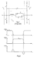
- Figure 1 describes a conventional sustain circuit for the electrical discharges in a plasma display panel. Such a circuit is notably described in the European Patent Application EP 0 704 834.
- This circuit comprises means 1 for applying a supply voltage Vs, alternately, to the sustain electrode Ys and the address-sustain electrode Yas of the plasma display cells and a circuit 2 designed to recover energy during the cell sustain phase.
- the means 1 consist of four switches I1, 12, 13 and 14. Two switches, I1 and 12, are connected in series between a power supply terminal receiving a sustain voltage Vs and ground. The mid-point between these two switches is connected to the electrode Ys of the display cells. The two other switches, 13 and 14, are also connected in series between the power supply terminal receiving the sustain voltage Vs and ground. The mid-point between these two switches is connected to the address-sustain electrode Yas of the cells.
- the energy recovery circuit 2 is connected between the electrodes Ys and Yas. It comprises an inductor L connected in series with a two-way switch between the electrodes Ys and Yas.
- the two-way switch is formed by a switch I5 in series with a diode D1 allowing the current to flow in one direction when the switch I5 is closed and, connected in parallel, by a switch 16 connected in series with a diode D2 allowing the current to flow in the opposite direction when the switch 16 is closed.
- the inductor L is connected in parallel with the capacitance C of the display (shown as a dotted line between the electrodes Ys and Yas) forming a resonant circuit with the latter.
- the detailed operation of this circuit is well known to those skilled in the art and is fully described in the European Patent Application EP 0 704 834.
- the energy recovery consists of a transfer of energy between the display capacitance and the inductor of the circuit 2 during voltage edges on the electrodes Ys and Yas. During a first edge, energy is transferred from the inductor to the capacitance of the display and, during the following edge, the energy transfer takes place in the opposite direction, i.e.
- the energy recovery takes place during a symmetric inversion of the potentials on the electrodes Ys and Yas. For example, when the potential on the electrode Ys goes from Vs to 0, the inverse transition is effected on the electrode Yas which goes from 0 to Vs.
- Figures 3 and 4 illustrate this impossibility.
- the capacitance C discharges into the inductor L, the potential of the electrode Yas decreases.
- the potential on the electrode Yas reaches 0 volts, the current stored in the inductor L is maximal.
- the invention aims to overcome the aforementioned drawbacks.
- the subject of the invention is a device for driving a plasma display panel comprising first means for generating a voltage falling edge on one of the sustain electrodes Ys and address-sustain electrodes Yas of the cells of said display, a fixed potential being maintained on the other of said sustain and address-sustain electrodes, characterized in that said first means store energy during a first time period of the falling edge and in that it additionally comprises second means for transferring the stored energy to the voltage supply source of the device during the remaining time period of said voltage falling edge.
- This device is compatible with the conventional cell sustain circuit of the plasma display.
- Said first means can notably be used for the sustain of the display cells.
- the first means of the device comprise an inductor of which a first end is connected to the electrode whose potential is decreased and a second end is connected to the electrode whose potential is kept fixed via a first diode connected in series with a switch, the anode of said first diode being on the side of said inductor, which switch is in a closed state during said first time period of the falling edge during which current is stored in the inductor and in an open state during the remaining time period of the falling edge during which the current stored in the inductor is transferred to the voltage supply source of the device.
- the second means consist, for example, of a second diode connected between said second end of the inductor and the voltage supply source of the device, the anode of said second diode being on the side of the second end of the inductor.
- the device additionally comprises a third diode in series with a resistor, the anode of said third diode being on the ground side, the whole assembly being connected between the second end of the inductor and ground.
- the device for driving the plasma display panel comprises means for generating a voltage falling edge on one of the sustain electrodes Ys and address-sustain electrodes Yas of the cells of said display, said means being designed to maintain a low potential on the other of said sustain and address-sustain electrodes and to store energy during a first period part of the falling edge, and second means for transferring the energy stored in the first means to the voltage supply source of the device during the end part of the falling edge.
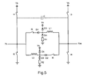
- FIG. 5 A circuit diagram of such a device is shown in Figure 5.
- This device is compatible with the sustain circuit of a conventional plasma display since certain elements of the device of the invention are employed both for the cell sustain and for generating a falling edge such as is claimed. These elements are designated by the same references in Figure 1 and in Figure 5.
- the driving device comprises an inductor L1 of which a first end is connected to the electrode Yas and a second end is connected to the electrode Ys via a diode D1 connected in series with a switch I5, the anode of the diode D1 being on the side of the inductor L1.
- a diode D4 in series with a resistor R1 is connected between ground and the second end of the inductor L1, with its anode on the ground side. The purpose of this diode and this resistor is to remove the negative flywheel current which could appear in the inductor L1 during the conventional sustain cycles of the display cells.
- the device of the invention also comprises means for generating a falling edge on the electrode Ys and for simultaneously maintaining a zero potential on the electrode Yas.
- the driving device also comprises an inductor L2 of which a first end is connected to the electrode Ys and a second end is connected to the electrode Yas via a diode D2 connected in series with a switch 16, the anode of the diode D2 being on the side of the inductor L2.
- a diode D5 is connected between the second end of the inductor L2 and the power source supplying the sustain voltage Vs.
- a diode D6 in series with a resistor R2 is connected between ground and the second end of the inductor L2, with its anode on the ground side.
- the operation of this other part of the circuit is identical to that comprising the elements L1, D1, 15, D3, D4 and R1, but with the direction of the currents and the potentials on the electrodes Ys and Yas inverted.
- the part of the circuit comprising the elements L1, D1, I5, D3, D4 and R1 operates in the following manner.
- the switch I5 is closed.
- a current loop is created through the inductor L1, the diode D1, the switch I5 and the display capacitance C.
- the inductor L1 becomes resonant with the display capacitance C and stores current up to a peak value Imax.
- the potential of the electrode Yas then decreases progressively.
- the switch I5 is then opened.
- the current stored in the inductor L1 is then extracted into the power supply Vs via the diode D3.
- the switch 12 is closed.
- a current loop through the inductor L1, the diode D3, the power source Vs, ground and the capacitance C is created.
- the potential of the electrode Yas continues to decrease to reach zero volts.
- the inductor L1 is fully discharged; current has been transferred to the power source of the device and the 2 electrodes Ys and Yas have reached zero potential.
- the elements L1, D1, I5 and L2, D2, 16 can be used for sustaining electrical discharges in the display cells as described in the document EP 0 704 834.
- the circuit now comprises two inductors, L1 and L2, each used in turn depending on the transition to be effected (0 ⁇ Vs or Vs ⁇ 0) instead of a single inductor, L, for all the transitions.
- this device presents the following advantages:
Landscapes
- Engineering & Computer Science (AREA)
- Physics & Mathematics (AREA)
- Power Engineering (AREA)
- Plasma & Fusion (AREA)
- Computer Hardware Design (AREA)
- General Physics & Mathematics (AREA)
- Theoretical Computer Science (AREA)
- Control Of Indicators Other Than Cathode Ray Tubes (AREA)
- Control Of Gas Discharge Display Tubes (AREA)
Abstract
Description
- Figure 1, described above, shows the circuit diagram of a cell sustain circuit of a prior-art plasma display;
- Figure 2, described above, shows the voltages applied to the electrodes Ys and Yas of the plasma display cells by the sustain circuit in Figure 1, together with the current flowing through the inductor L of the circuit during the voltage rising and falling edges;
- Figures 3 and 4, described above, show the currents flowing in the circuit of Figure 1 in the case where it is desired to decrease the voltage Vs to 0 volts on the electrode Yas of the display cells while simultaneously maintaining the electrode Ys at 0 volts;
- Figure 5 shows a circuit diagram of a device, according to the invention, capable of generating a voltage falling edge on one of the electrodes Ys or Yas of the display cells, while simultaneously maintaining a fixed potential on the other electrode;
- Figures 6 or 7 show the currents flowing in the circuit of Figure 5 during the generation of the falling edge on the electrode Yas of the plasma display cells, the potential on the electrode Ys being maintained at 0 volts; and
- Figure 8 is a set of timing diagrams showing the behaviour of the currents and voltages in the elements of the circuit in Figure 5 during the generation of a falling edge on the electrode Yas of the plasma display cells.
- the elements L1, D1, I5, L2, D2 and 16 can be used as an energy recovery circuit (allowing energy to be transferred from the inductor to the display capacitance and vice versa) during the sustain phase of the plasma display cells;
- little thermal losses are created;
- its cost of implementation is very low given that it can also serve as an energy recovery circuit during the sustain phase of the display cells.
Claims (4)
- Device for driving a plasma display panel comprising first means (L1, D1, I5 or L2, D2, 16) for generating a voltage falling edge on one of the sustain electrodes (Ys) and address-sustain electrodes (Yas) of the cells of said display, a fixed potential being maintained on the other of said sustain and address-sustain electrodes, characterized in that said first means store energy during a first time period of the falling edge and in that said driving device additionally comprises second means (D3) for transferring said stored energy to the voltage supply source of the device during the remaining time period of said falling edge.
- Device according to claim 1, characterized in that said first means comprise an inductor (L1 or L2) of which a first end is connected to the electrode whose potential is decreased and a second end is connected to the electrode whose potential is kept fixed via a first diode (D1 or D2) connected in series with a switch (I5 or 16), the anode of said first diode being on the side of said inductor, which switch is in a closed state during said first time period of the falling edge during which current is stored in the inductor (L1 or L2) and in an open state during the remaining time period of the falling edge during which the current stored in the inductor is transferred to the voltage supply source of the device.
- Device according to claim 2, characterized in that the second means consist of a second diode (D3 or D5) connected between said second end of the inductor (L1 or L2) and the voltage supply source of the device, the anode of said second diode (D3 or D5) being on the side of the second end of the inductor.
- Device according to Claim 3, characterized in that it additionally comprises a third diode (D4 or D6) in series with a resistor (R1 or R2), the anode of said third diode (D4 or D6) being on the ground side, the whole assembly being connected between the second end of the inductor (L1 or L2) and ground.
Applications Claiming Priority (2)
| Application Number | Priority Date | Filing Date | Title |
|---|---|---|---|
| FR0309967A FR2858872A1 (en) | 2003-08-14 | 2003-08-14 | GENERATION OF DESCENDING FRONTS WITH ENERGY RECOVERY IN A PLASMA PANEL |
| FR0309967 | 2003-08-14 |
Publications (2)
| Publication Number | Publication Date |
|---|---|
| EP1507250A2 true EP1507250A2 (en) | 2005-02-16 |
| EP1507250A3 EP1507250A3 (en) | 2007-12-12 |
Family
ID=33561180
Family Applications (1)
| Application Number | Title | Priority Date | Filing Date |
|---|---|---|---|
| EP04018256A Withdrawn EP1507250A3 (en) | 2003-08-14 | 2004-08-02 | Generation of falling edges with energy recovery in a plasma display |
Country Status (7)
| Country | Link |
|---|---|
| US (1) | US20050035930A1 (en) |
| EP (1) | EP1507250A3 (en) |
| JP (1) | JP2005062873A (en) |
| KR (1) | KR20050019051A (en) |
| CN (1) | CN1581263A (en) |
| FR (1) | FR2858872A1 (en) |
| TW (1) | TW200509031A (en) |
Cited By (2)
| Publication number | Priority date | Publication date | Assignee | Title |
|---|---|---|---|---|
| EP1901271A1 (en) * | 2006-09-12 | 2008-03-19 | LG Electronics Inc. | Plasma display apparatus |
| EP1906380A1 (en) * | 2006-09-29 | 2008-04-02 | LG Electronics Inc. | Plasma display apparatus |
Families Citing this family (3)
| Publication number | Priority date | Publication date | Assignee | Title |
|---|---|---|---|---|
| US7352344B2 (en) * | 2005-04-20 | 2008-04-01 | Chunghwa Picture Tubes, Ltd. | Driver circuit for plasma display panels |
| US7385569B2 (en) * | 2005-06-22 | 2008-06-10 | Chunghwa Picture Tubes, Ltd. | Driving circuit of plasma display panel |
| CN101441846B (en) * | 2007-11-19 | 2011-09-07 | 四川虹欧显示器件有限公司 | Energy recovery apparatus based on insulated gate bipolar transistor |
Family Cites Families (9)
| Publication number | Priority date | Publication date | Assignee | Title |
|---|---|---|---|---|
| US4638218A (en) * | 1983-08-24 | 1987-01-20 | Fujitsu Limited | Gas discharge panel and method for driving the same |
| US5081400A (en) * | 1986-09-25 | 1992-01-14 | The Board Of Trustees Of The University Of Illinois | Power efficient sustain drivers and address drivers for plasma panel |
| JP3364066B2 (en) * | 1995-10-02 | 2003-01-08 | 富士通株式会社 | AC-type plasma display device and its driving circuit |
| JP3241577B2 (en) * | 1995-11-24 | 2001-12-25 | 日本電気株式会社 | Display panel drive circuit |
| CA2220342A1 (en) * | 1996-03-26 | 1997-10-02 | Fourie, Inc. | Display device |
| JP3897896B2 (en) * | 1997-07-16 | 2007-03-28 | 三菱電機株式会社 | Plasma display panel driving method and plasma display device |
| TW589602B (en) * | 2001-09-14 | 2004-06-01 | Pioneer Corp | Display device and method of driving display panel |
| JP2003114640A (en) * | 2001-10-04 | 2003-04-18 | Nec Corp | Plasma display panel and its driving method |
| FR2832538A1 (en) * | 2001-11-22 | 2003-05-23 | Thomson Licensing Sa | Impulse generator for a plasma display panel for generation of image maintenance pulses has an array of parallel switching and recuperation modules that enable the recuperation of capacitive energy |
-
2003
- 2003-08-14 FR FR0309967A patent/FR2858872A1/en active Pending
-
2004
- 2004-08-02 EP EP04018256A patent/EP1507250A3/en not_active Withdrawn
- 2004-08-09 US US10/915,606 patent/US20050035930A1/en not_active Abandoned
- 2004-08-11 JP JP2004234767A patent/JP2005062873A/en not_active Withdrawn
- 2004-08-11 KR KR1020040063144A patent/KR20050019051A/en not_active Withdrawn
- 2004-08-12 CN CNA2004100574712A patent/CN1581263A/en active Pending
- 2004-08-12 TW TW093124139A patent/TW200509031A/en unknown
Cited By (4)
| Publication number | Priority date | Publication date | Assignee | Title |
|---|---|---|---|---|
| EP1901271A1 (en) * | 2006-09-12 | 2008-03-19 | LG Electronics Inc. | Plasma display apparatus |
| US7999764B2 (en) | 2006-09-12 | 2011-08-16 | Lg Electronics Inc. | Plasma display apparatus |
| EP1906380A1 (en) * | 2006-09-29 | 2008-04-02 | LG Electronics Inc. | Plasma display apparatus |
| US7852290B2 (en) | 2006-09-29 | 2010-12-14 | Lg Electronics Inc. | Plasma display apparatus |
Also Published As
| Publication number | Publication date |
|---|---|
| FR2858872A1 (en) | 2005-02-18 |
| TW200509031A (en) | 2005-03-01 |
| KR20050019051A (en) | 2005-02-28 |
| EP1507250A3 (en) | 2007-12-12 |
| US20050035930A1 (en) | 2005-02-17 |
| CN1581263A (en) | 2005-02-16 |
| JP2005062873A (en) | 2005-03-10 |
Similar Documents
| Publication | Publication Date | Title |
|---|---|---|
| EP2149896B1 (en) | Relay driving circuit and battery pack using same | |
| JP5042433B2 (en) | Driving device and driving method for plasma display panel | |
| US7161564B2 (en) | Apparatus and method for driving a plasma display panel | |
| US20020047577A1 (en) | Energy recovery sustain circuit for AC plasma display panel | |
| US20050012690A1 (en) | Plasma display panel and method for driving the same | |
| JP2004513398A (en) | Energy recovery circuit with boost function and energy efficiency method using it | |
| JP2009176749A (en) | Electronic circuit | |
| WO1991012703A1 (en) | Light-emitting power source circuit | |
| JP2751951B2 (en) | Display panel drive circuit | |
| US20050035930A1 (en) | Generation of falling edges with energy recovery in a plasma display | |
| JP4233873B2 (en) | Electronic circuit | |
| JPH1115426A (en) | Capacitive load drive circuit | |
| US20030132712A1 (en) | Electroluminescent driver circuit | |
| JP3351381B2 (en) | Display device charge recovery method | |
| JP4403729B2 (en) | Display device | |
| EP0899988B1 (en) | Electroluminescent lamp driver circuit with signal tracking | |
| JP2024118535A (en) | Charging circuit | |
| US6341077B1 (en) | Boosting circuit | |
| US20060267872A1 (en) | Plasma display panel driver circuit having two-direction energy recovery through one switch | |
| US7348941B2 (en) | Driving circuit of plasma display panel | |
| EP1646143A1 (en) | Amplifier designed to generate a rectangular voltage signal with soft switching on a capacitive load | |
| EP1505561B1 (en) | Control device in a plasma display panel | |
| KR100792447B1 (en) | Driving Circuit of Plasma Display Panel | |
| US8115701B2 (en) | Sustain device for plasma panel | |
| Kwak | Simplified sustain driver with low-voltage semiconductor devices and low-voltage power supply for AC plasma display panel |
Legal Events
| Date | Code | Title | Description |
|---|---|---|---|
| PUAI | Public reference made under article 153(3) epc to a published international application that has entered the european phase |
Free format text: ORIGINAL CODE: 0009012 |
|
| AK | Designated contracting states |
Kind code of ref document: A2 Designated state(s): AT BE BG CH CY CZ DE DK EE ES FI FR GB GR HU IE IT LI LU MC NL PL PT RO SE SI SK TR |
|
| AX | Request for extension of the european patent |
Extension state: AL HR LT LV MK |
|
| RAP1 | Party data changed (applicant data changed or rights of an application transferred) |
Owner name: THOMSON LICENSING |
|
| PUAL | Search report despatched |
Free format text: ORIGINAL CODE: 0009013 |
|
| STAA | Information on the status of an ep patent application or granted ep patent |
Free format text: STATUS: THE APPLICATION HAS BEEN WITHDRAWN |
|
| AK | Designated contracting states |
Kind code of ref document: A3 Designated state(s): AT BE BG CH CY CZ DE DK EE ES FI FR GB GR HU IE IT LI LU MC NL PL PT RO SE SI SK TR |
|
| AX | Request for extension of the european patent |
Extension state: AL HR LT LV MK |
|
| 18W | Application withdrawn |
Effective date: 20071102 |