EP1505657A1 - Vertical semiconductor device and manufacturing method thereof - Google Patents
Vertical semiconductor device and manufacturing method thereof Download PDFInfo
- Publication number
- EP1505657A1 EP1505657A1 EP04018303A EP04018303A EP1505657A1 EP 1505657 A1 EP1505657 A1 EP 1505657A1 EP 04018303 A EP04018303 A EP 04018303A EP 04018303 A EP04018303 A EP 04018303A EP 1505657 A1 EP1505657 A1 EP 1505657A1
- Authority
- EP
- European Patent Office
- Prior art keywords
- main surface
- semiconductor substrate
- region
- trench
- conductivity type
- Prior art date
- Legal status (The legal status is an assumption and is not a legal conclusion. Google has not performed a legal analysis and makes no representation as to the accuracy of the status listed.)
- Granted
Links
Images



Classifications
-
- H—ELECTRICITY
- H10—SEMICONDUCTOR DEVICES; ELECTRIC SOLID-STATE DEVICES NOT OTHERWISE PROVIDED FOR
- H10D—INORGANIC ELECTRIC SEMICONDUCTOR DEVICES
- H10D12/00—Bipolar devices controlled by the field effect, e.g. insulated-gate bipolar transistors [IGBT]
- H10D12/411—Insulated-gate bipolar transistors [IGBT]
- H10D12/441—Vertical IGBTs
-
- H—ELECTRICITY
- H10—SEMICONDUCTOR DEVICES; ELECTRIC SOLID-STATE DEVICES NOT OTHERWISE PROVIDED FOR
- H10D—INORGANIC ELECTRIC SEMICONDUCTOR DEVICES
- H10D12/00—Bipolar devices controlled by the field effect, e.g. insulated-gate bipolar transistors [IGBT]
- H10D12/01—Manufacture or treatment
-
- H—ELECTRICITY
- H10—SEMICONDUCTOR DEVICES; ELECTRIC SOLID-STATE DEVICES NOT OTHERWISE PROVIDED FOR
- H10D—INORGANIC ELECTRIC SEMICONDUCTOR DEVICES
- H10D30/00—Field-effect transistors [FET]
- H10D30/60—Insulated-gate field-effect transistors [IGFET]
- H10D30/64—Double-diffused metal-oxide semiconductor [DMOS] FETs
- H10D30/66—Vertical DMOS [VDMOS] FETs
- H10D30/668—Vertical DMOS [VDMOS] FETs having trench gate electrodes, e.g. UMOS transistors
-
- H—ELECTRICITY
- H10—SEMICONDUCTOR DEVICES; ELECTRIC SOLID-STATE DEVICES NOT OTHERWISE PROVIDED FOR
- H10D—INORGANIC ELECTRIC SEMICONDUCTOR DEVICES
- H10D62/00—Semiconductor bodies, or regions thereof, of devices having potential barriers
- H10D62/10—Shapes, relative sizes or dispositions of the regions of the semiconductor bodies; Shapes of the semiconductor bodies
- H10D62/102—Constructional design considerations for preventing surface leakage or controlling electric field concentration
- H10D62/103—Constructional design considerations for preventing surface leakage or controlling electric field concentration for increasing or controlling the breakdown voltage of reverse-biased devices
- H10D62/104—Constructional design considerations for preventing surface leakage or controlling electric field concentration for increasing or controlling the breakdown voltage of reverse-biased devices having particular shapes of the bodies at or near reverse-biased junctions, e.g. having bevels or moats
-
- H—ELECTRICITY
- H10—SEMICONDUCTOR DEVICES; ELECTRIC SOLID-STATE DEVICES NOT OTHERWISE PROVIDED FOR
- H10D—INORGANIC ELECTRIC SEMICONDUCTOR DEVICES
- H10D62/00—Semiconductor bodies, or regions thereof, of devices having potential barriers
- H10D62/10—Shapes, relative sizes or dispositions of the regions of the semiconductor bodies; Shapes of the semiconductor bodies
- H10D62/102—Constructional design considerations for preventing surface leakage or controlling electric field concentration
- H10D62/103—Constructional design considerations for preventing surface leakage or controlling electric field concentration for increasing or controlling the breakdown voltage of reverse-biased devices
- H10D62/105—Constructional design considerations for preventing surface leakage or controlling electric field concentration for increasing or controlling the breakdown voltage of reverse-biased devices by having particular doping profiles, shapes or arrangements of PN junctions; by having supplementary regions, e.g. junction termination extension [JTE]
-
- H—ELECTRICITY
- H10—SEMICONDUCTOR DEVICES; ELECTRIC SOLID-STATE DEVICES NOT OTHERWISE PROVIDED FOR
- H10D—INORGANIC ELECTRIC SEMICONDUCTOR DEVICES
- H10D64/00—Electrodes of devices having potential barriers
- H10D64/01—Manufacture or treatment
- H10D64/011—Manufacture or treatment of electrodes ohmically coupled to a semiconductor
- H10D64/0111—Manufacture or treatment of electrodes ohmically coupled to a semiconductor to Group IV semiconductors
- H10D64/0113—Manufacture or treatment of electrodes ohmically coupled to a semiconductor to Group IV semiconductors the conductive layers comprising highly doped semiconductor materials, e.g. polysilicon layers or amorphous silicon layers
-
- H—ELECTRICITY
- H10—SEMICONDUCTOR DEVICES; ELECTRIC SOLID-STATE DEVICES NOT OTHERWISE PROVIDED FOR
- H10P—GENERIC PROCESSES OR APPARATUS FOR THE MANUFACTURE OR TREATMENT OF DEVICES COVERED BY CLASS H10
- H10P30/00—Ion implantation into wafers, substrates or parts of devices
- H10P30/20—Ion implantation into wafers, substrates or parts of devices into semiconductor materials, e.g. for doping
- H10P30/202—Ion implantation into wafers, substrates or parts of devices into semiconductor materials, e.g. for doping characterised by the semiconductor materials
- H10P30/204—Ion implantation into wafers, substrates or parts of devices into semiconductor materials, e.g. for doping characterised by the semiconductor materials into Group IV semiconductors
- H10P30/2042—Ion implantation into wafers, substrates or parts of devices into semiconductor materials, e.g. for doping characterised by the semiconductor materials into Group IV semiconductors into crystalline silicon carbide
-
- H—ELECTRICITY
- H10—SEMICONDUCTOR DEVICES; ELECTRIC SOLID-STATE DEVICES NOT OTHERWISE PROVIDED FOR
- H10P—GENERIC PROCESSES OR APPARATUS FOR THE MANUFACTURE OR TREATMENT OF DEVICES COVERED BY CLASS H10
- H10P32/00—Diffusion of dopants within, into or out of wafers, substrates or parts of devices
-
- H—ELECTRICITY
- H10—SEMICONDUCTOR DEVICES; ELECTRIC SOLID-STATE DEVICES NOT OTHERWISE PROVIDED FOR
- H10P—GENERIC PROCESSES OR APPARATUS FOR THE MANUFACTURE OR TREATMENT OF DEVICES COVERED BY CLASS H10
- H10P50/00—Etching of wafers, substrates or parts of devices
- H10P50/60—Wet etching
- H10P50/64—Wet etching of semiconductor materials
- H10P50/642—Chemical etching
- H10P50/644—Anisotropic liquid etching
-
- H—ELECTRICITY
- H10—SEMICONDUCTOR DEVICES; ELECTRIC SOLID-STATE DEVICES NOT OTHERWISE PROVIDED FOR
- H10W—GENERIC PACKAGES, INTERCONNECTIONS, CONNECTORS OR OTHER CONSTRUCTIONAL DETAILS OF DEVICES COVERED BY CLASS H10
- H10W20/00—Interconnections in chips, wafers or substrates
- H10W20/01—Manufacture or treatment
- H10W20/071—Manufacture or treatment of dielectric parts thereof
- H10W20/074—Manufacture or treatment of dielectric parts thereof of dielectric parts comprising thin functional dielectric layers, e.g. dielectric etch-stop, barrier, capping or liner layers
- H10W20/076—Manufacture or treatment of dielectric parts thereof of dielectric parts comprising thin functional dielectric layers, e.g. dielectric etch-stop, barrier, capping or liner layers in via holes or trenches
Definitions
- the present invention relates to a semiconductor device such as an IGBT (Insulated Gate Bipolar Transistor) having a bidirectional breakdown voltage and a manufacturing method thereof, and more particularly to a peripheral breakdown voltage structure in the semiconductor device.
- IGBT Insulated Gate Bipolar Transistor
- a reverse blocking IGBT as illustrated in Fig. 1 of Japanese Patent Application Laid-Open No. 2002-319676 (pages 7 to 8, Fig. 1).
- This kind of reverse blocking IGBT requires a p+ region obtained by diffusing boron to a depth of 120 ⁇ m in an oxygen atmosphere at a temperature of 1200°C or more to lie on the periphery of a chip in order to maintain a reverse breakdown voltage, and thus needs a long-diffusion process.
- horizontal diffusion of the boron causes the p + region to spread over a chip surface to the almost same degree as the diffusion depth, resulting in a considerable reduction in utilization efficiency of the chip surface.
- Japanese Patent Application Laid-Open No. 2001-185727 proposes a reverse blocking IGBT having such a structure as shown in Fig. 15(c).
- This IGBT provides an inclined trench in a portion corresponding to the p + region of the IGBT disclosed in the aforementioned publication using side etching by isotropic wet etching to form a positive bevel structure, and introduces an impurity by diffusion from a wall surface of the trench to provide p+ regions. While this IGBT eliminates the need for a long-diffusion process as in the IGBT disclosed in the aforementioned publication, it does need a trench width in accordance with the inclination because the trench needs to be inclined. This too has considerably reduced utilization efficiency of a chip surface.
- a vertical semiconductor device includes a semiconductor substrate, a first impurity region, a trench and a second impurity region.
- the semiconductor substrate includes a first main surface and a second main surface opposed to the first main surface and is of a first conductivity type.
- the semiconductor substrate further includes an element region and a peripheral region provided so as to surround the element region.
- the first impurity region is formed inside the semiconductor substrate so as to be exposed at the second main surface, and has a higher impurity concentration higher than the first conductivity type of the semiconductor substrate.
- the trench is provided in the peripheral region and has an almost vertical sidewall with reference to the first main surface.
- the second impurity region is formed along the sidewall of the trench inside of the semiconductor substrate in a prescribed thickness, and is of a second conductivity type electrically connected to the first impurity region.
- a ratio d/w (aspect ratio) between a depth d and an opening width w of the trench is 5 or more and 10 or less.
- Figs. 1 and 2 illustrate configurations of a reverse blocking IGBT having a breakdown voltage of 600V according to a first preferred embodiment.
- Fig. 1 is a plan view of a chip used in the reverse blocking IGBT and
- Fig. 2 is a sectional view taken along the line A-A' on a peripheral portion of the chip.
- An n-type silicon substrate 1 includes parallel and opposed first and second main surfaces, and a p-type collector layer 2 (first impurity region) of a high concentration is provided to form a PN junction with the silicon substrate 1 by introducing a p-type impurity e.g., boron from the second main surface side.
- a collector electrode 8 is formed on the p-type collector layer 2.
- a central portion of the chip in Fig. 1 is an element region RE, which is filled with a plurality of IGBT cells 30 and is responsible for a main operation of the IGBT.
- a peripheral region RP is provided to surround the element region RE.
- a p-type base region 3 is formed in the semiconductor substrate 1 so as to be partially exposed at the first main surface.
- N-type emitter regions 4 are formed in the p-type base region 3 so as also to be partially exposed at the first main surface.
- a gate electrode 6 made of polycrystalline silicon is provided through a gate insulating film 5 made of silicon dioxide on the exposed portions of the base region 3 between the semiconductor substrate 1 and the emitter region 4.
- an emitter electrode 7 is provided on the first main surface so as to make electrical contact with the base region 3 and the emitter regions 4.
- Each IGBT cell 30 consists of the p-type base region 3, the n-type emitter regions 4, the gate insulating film 5, the gate electrode 6, the emitter electrode 7, the silicon substrate 1, the p-type collector layer 2 and the collector electrode 8.
- a peripheral base region 9, a guard ring 10 and a guard ring electrode 11 are formed to partially constitute the peripheral region RP.
- An insulating film 12 is formed on the first main surface covering the peripheral region RP for protective purposes. The peripheral region RP is responsible for maintaining the breakdown voltage of the IGBT.
- a trench 13 is formed in an outer edge portion of the peripheral region RP so as to reach the p-type collector layer 2 from the first main surface of the silicon substrate 1.
- the trench 13 is arranged continuously so as to surround the element region RE. Between sidewalls of the trench 13, the one close to the element region RE is called a first sidewall, and the other one far from the element region RE is called a second sidewall hereafter. While the trench 13 surrounds the element region RE to form a square in Fig. 1, the trench 13 may surround the element region RE to form another shape as required, by rounding corner portions of the square, for example.
- a depth of the PN junction between the semiconductor substrate 1 and the p-type collector layer 2 from the first main surface is approximately 100 ⁇ m. Accordingly, a depth of the trench 13 needs to be 100 ⁇ m or more. In the first preferred embodiment, the depth of the trench 13 is set to be 110 ⁇ m.
- a p-type isolation region 14 (second impurity region) of about 5 ⁇ m thickness is formed along wall surfaces of the trench 13. At this time, p-type isolation regions 14a and 14b are formed on the first and second sidewalls sides of the trench 13, respectively.
- the mere "p-type isolation region 14" mentioned in the present specification includes both the p-type isolation regions 14a and 14b on the first and second sidewalls sides, respectively.
- the trench 13 including the p-type isolation region 14 is filled with a filling material 16. Since the depth of the trench 13 is set to reach the collector layer 2, the p-type isolation region 14 is electrically connected to the collector layer 2.
- a p-type impurity concentration of the p-type isolation region 14 be 1 ⁇ 10 14 atoms/cm 3 or more, preferably 1 ⁇ 10 15 atoms/cm 3 or more, in surface concentration at an interface with the filling material 16.
- the surface concentration is less than 1 ⁇ 10 14 atoms/cm 3
- a field plate 15 made of aluminum is provided on the first main surface to make contact with the p-type isolation region 14. While filling the trench 13 is not necessarily needed, it is desirable that the filling material 16 should be formed by filling the trench 13 with some material in order to avoid contamination stemming from residues of a resist and the like used in a wafer process.
- silicon dioxide is used for the filling material 16 because of its high deposition rate. Considering stress of the filling material 16 to be applied to the silicon substrate 1, however, it is further desirable to use a material having a slower deposition rate yet an approximate modulus of thermal expansion to the silicon substrate, i.e., molybdenum, tungsten or polycrystalline silicon, or a composite of those materials.
- the reverse blocking IGBT mentioned above is manufactured as explained hereafter.
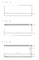
- a p-type impurity e.g., boron is introduced from the second main surface to entirely form the p-type collector layer 2 (Fig. 3).
- a TEOS film 20 is deposited as a mask material on the first main surface of the silicon substrate 1, and a prescribed opening is formed in the TEOS film 20 using photolithography (Fig. 4).
- the TEOS film is a silicon dioxide film formed by CVD with TEOS (Tetra Ethyl Ortho Silicate) as a silicon source.
- the trench 13 having the prescribed depth and opening width is so formed as to reach the p-type collector layer 2 from the first main surface of the silicon substrate 1 by anisotropic etching using the opening (Fig. 5).
- the trench 13 is set to be 110 ⁇ m deep.
- a trench width inevitably extends twice as much as the trench depth to almost 200 ⁇ m due to side etching on both sides.
- the trench 13 is formed by anisotropic etching e.g., ICP (Inductive Coupled Plasma) etching. Therefore, the opening width reaches as small as approximately 3 ⁇ m in the first preferred embodiment.
- the ICP etching is capable of forming a trench with an aspect ratio of up to approximately 100, the aspect ratio being a ratio d/w between a trench depth d and a trench opening width w.
- the aspect ratio of the first preferred embodiment is approximately 40 (the opening width is approximately 2.75).
- An opening width may be set to be 20 ⁇ m or less when the aspect ratio of 5 is or larger, which means that the opening width may be narrowed to be approximately one-tenth part of that when isotropic etching is used.
- ion implantation and subsequent diffusion by annealing are performed through the opening while leaving the TEOS film 20 as it is, to introduce boron the p-type impurity from the trench sidewall, thereby forming the p-type isolation region 14 having the prescribed thickness from the trench sidewall surface in the silicon substrate 1 around the trench 13 (Fig. 6).
- the ion implantation is performed by an oblique ion implantation method which implants ions at a certain angle ⁇ inclined with reference to the normal (line) of the first main surface.
- the p-type isolation region 14 may be formed by a coating diffusion method or a gas diffusion method instead of the above ion implantation diffusion method, when applied to form a trench having a small opening and a great depth as in the first preferred embodiment, the coating diffusion method and the gas diffusion method present a problem such that it is hard to provide the impurity atoms to as far as the bottom of the trench and thus a uniform impurity concentration becomes unobtainable.
- the first preferred embodiment which employs the ion implantation diffusion method, obtains the p-type isolation region 14 of a uniform impurity concentration without presenting such problem.
- a tangent of the incident angle ⁇ of the ion implantation i.e., tan ⁇
- the impurity ions are applied to as far as the bottom of the trench, and a uniform concentration distribution can be obtained across the whole trench sidewalls.
- silicon dioxide is deposited entirely on the first main surface of the semiconductor substrate 1 by CVD so as to completely fill the trench, after the TEOS film 20 is removed.
- the silicon dioxide deposited over the first main surface is then removed by etching such that the silicon oxide remains only in the trench. Consequently, the filling material 16 made of silicon dioxide is completed in the trench (Fig. 7).
- the filling material 16 may be similarly formed of polycrystalline silicon or a metal such as molybdenum and tungsten, or a composite of those materials.
- the base region 3, the emitter regions 4, the gate insulating film 5, the gate electrode 6, the emitter electrode 7, the collector electrode 8, the peripheral base region 9 and others are formed by a well-known manufacturing method of an IGBT cell, completing the reverse blocking IGBT according to the first preferred embodiment.
- a depletion layer generated around the PN junction between the collector layer 2 and the semiconductor substrate 1 is extended toward the semiconductor substrate 1 side, allowing a reverse breakdown voltage to be maintained.
- a depletion layer is also generated around a PN junction between the p-type isolation region 14 continuous with the collector layer 2 and the semiconductor layer 1, yet it is extended only toward the semiconductor substrate 1 side and not extended up to an outer edge of the chip outside the p-type isolation region 14. This prevents an electric field from being developed up to a dicing line at the outer edge of the chip, thereby stabilizing the reverse breakdown voltage.
- the depletion layer generated around the PN junction between the p-type isolation region 14 and the semiconductor layer 1 is slightly extended to the inside of the p-type isolation region 14 to make contact with the field plate 15, leading to deterioration of the breakdown voltage.
- the p-type isolation region 14 is formed by impurity diffusion from the sidewall of the trench that is formed on the peripheral portion of the chip by anisotropic etching. Therefore, a proportion of the p-type isolation region 14 occupying the chip area can be reduced, improving utilization efficiency of the chip surface.
- the trench 13 is so formed as to reach the collector layer 2 in the first preferred embodiment, it is essential only that the p-type isolation region 14 and the collector layer 2 be connected and have the same potential in order to attain the object of the present invention.
- a modification of the present invention is given as illustrated in Fig. 8.
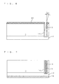
- the trench 13 in Fig. 8 is identical to that in Fig. 2 except that the bottom thereof does not reach the collector layer 2.
- the depth of the PN junction between the semiconductor substrate 1 and the p-type collector layer 2 from the first main surface is approximately 100 ⁇ m and the depth of the trench 13 is set to be 95 ⁇ m.
- the p-type isolation region 14 formed along the wall surfaces of the trench 13 has a thickness of approximately 5 ⁇ m, so that the p-type isolation region 14 and the collector layer 2 are electrically connected to each other.
- the modification illustrated in Fig. 8 produces similar functions and effect.
- the trench 13 is shallower in the modification in Fig. 8, the occurrence of crystal defects resulting from the stress by the filling material 16 to be filled in the trench 13 is suppressed in the semiconductor substrate 1.
- the thickness of the semiconductor substrate 1 after the trench 13 has been formed can be ensured to a sufficient degree, so that mechanical strength of the semiconductor substrate 1 can be ensured, preventing damage at the time of handling.
- Fig. 9 illustrates a configuration of a reverse blocking IGBT according to a second preferred embodiment.
- a plan view of a chip is identical to that of Fig. 1 according to the first preferred embodiment, and Fig. 9 is a sectional view taken along the line A-A' on the peripheral portion of the chip.
- This configuration is different from that of Fig. 2 according to the first preferred embodiment in that the p-type isolation region 14 is omitted and silicon doped with a p-type impurity (e.g. boron) is used as a filling material 17 instead. Consequently, the filling material 17 servers the functions of the p-type isolation region 14 in the first preferred embodiment. Therefore, a reverse blocking IGBT having the same effect as in the first preferred embodiment yet being more simply configured can be obtained without providing an additional p-type isolation region.
- a p-type impurity e.g. boron
- the manufacturing method in the second preferred embodiment is omitted here because it is identical to that in the first preferred embodiment except that the step of forming the p-type isolation region 14 is omitted.
- the p-type impurity included in the filling material 17 may diffuse into the semiconductor substrate 1 to form a p-type diffusion layer around the trench 13, achieving the same structure as that of the first preferred embodiment. Needless to say, this produces the beneficial effect as in the first preferred embodiment in term of simplifying the manufacturing method by omitting the step of forming the p-type isolation region 14.
- Fig. 10 is a plan view of a chip used in a reverse blocking IGBT having a breakdown voltage of 600V according to the third preferred embodiment.
- a sectional view taken along the line A-A' on the peripheral portion of the chip is identical to that of Fig. 2 and is thus omitted.
- Figs. 11 and 12 are views illustrating a portion B in Fig. 10 in an enlarged manner.
- the trench 13 which is provided on the peripheral region as a single trench so as to continuously surround the element region RE in Fig. 1, is provided as a plurality of trenches so as to intermittently surround the element region RE in Fig. 10.
- the p-type isolation regions 14 are formed around the sidewalls of the plurality of the trenches and the adjacent p-type isolation regions 14 are separated by a distance W.
- each of depletion layers generated around PN junctions between the plurality of the p-type isolation regions 14 continuous with the collector layer 2 and the semiconductor substrate 1 depletes the semiconductor substrate 1 between the plurality of the p-type isolation regions 14 with a relatively low voltage level.
- Those depletion layers are extended only toward the element region RE side in the semiconductor substrate 1 even when the voltage level is increased afterward. Accordingly, a high voltage is not applied up to the outer edge of the chip outside the p-type isolation regions 14.
- Fig. 13 is a graph showing a relation between the distance W of the p-type isolation regions 14 and a reverse breakdown voltage between a collector electrode and an emitter electrode.
- the vertical axis indicates a reverse breakdown voltage between a collector electrode and an emitter electrode of an IGBT and the horizontal axis indicates the distance W.
- the p-type isolation regions 14 are formed on conditions of boron implantation at 50KeV and at 1 ⁇ 10 15 atoms/cm 2 and an annealing process for 30 minutes at 1215°C, the distance W is divided from 0 to 40 ⁇ m, device structure data is prepared with a process simulator called tsuprem4, and then a breakdown voltage of each structure is calculated by a calculator based on the structure data with a device simulator called Medici.
- Fig. 13 indicates a sharp decrease in the reverse breakdown of the IGBT after the distance W reaches more than 15 ⁇ m. Therefore, we learn that the IGBT should be designed with the distance W smaller than or equal to 15 ⁇ m.
- the vertical semiconductor devices are defined as a reverse blocking IGBT, and the first and second conductivity types are defined as n-type and p-type, respectively. Meanwhile, the functions and effect remain unchanged with the reversed conductivity types.
Landscapes
- Element Separation (AREA)
- Thyristors (AREA)
- Electrodes Of Semiconductors (AREA)
- Bipolar Transistors (AREA)
Abstract
Description
- The present invention relates to a semiconductor device such as an IGBT (Insulated Gate Bipolar Transistor) having a bidirectional breakdown voltage and a manufacturing method thereof, and more particularly to a peripheral breakdown voltage structure in the semiconductor device.
- In recent years a power conversion circuit, the so-called AC matrix converter, which is switched on and off directly by a bidirectional switch has been proposed to be used in a semiconductor power conversion device. And a semiconductor device having a bidirectional breakdown voltage has been called for as the bidirectional switch used in the AC matrix converter.
- One conventional example of such semiconductor device is a reverse blocking IGBT as illustrated in Fig. 1 of Japanese Patent Application Laid-Open No. 2002-319676 (
pages 7 to 8, Fig. 1). This kind of reverse blocking IGBT, however, requires a p+ region obtained by diffusing boron to a depth of 120 µm in an oxygen atmosphere at a temperature of 1200°C or more to lie on the periphery of a chip in order to maintain a reverse breakdown voltage, and thus needs a long-diffusion process. Besides, horizontal diffusion of the boron causes the p + region to spread over a chip surface to the almost same degree as the diffusion depth, resulting in a considerable reduction in utilization efficiency of the chip surface. - In order to address those problems, Japanese Patent Application Laid-Open No. 2001-185727 (
page 7, Fig. 15) proposes a reverse blocking IGBT having such a structure as shown in Fig. 15(c). This IGBT provides an inclined trench in a portion corresponding to the p + region of the IGBT disclosed in the aforementioned publication using side etching by isotropic wet etching to form a positive bevel structure, and introduces an impurity by diffusion from a wall surface of the trench to provide p+ regions. While this IGBT eliminates the need for a long-diffusion process as in the IGBT disclosed in the aforementioned publication, it does need a trench width in accordance with the inclination because the trench needs to be inclined. This too has considerably reduced utilization efficiency of a chip surface. - The terminal structures disclosed in the Japanese Patent Application Laid-Open Nos. 2002-319676 and 2001-185727 both require a considerable area of the chip to form the structure for maintaining the reverse breakdown voltage, resulting in a considerable reduction in utilization efficiency of the chip surface. This has caused an increase in chip size, which in turn has increased the chip cost.
- It is an object of the present invention to obtain a vertical semiconductor device including a terminal structure capable of improving utilization efficiency of a chip area while maintaining a reverse breakdown voltage.
- According to the present invention, a vertical semiconductor device includes a semiconductor substrate, a first impurity region, a trench and a second impurity region. The semiconductor substrate includes a first main surface and a second main surface opposed to the first main surface and is of a first conductivity type. The semiconductor substrate further includes an element region and a peripheral region provided so as to surround the element region. The first impurity region is formed inside the semiconductor substrate so as to be exposed at the second main surface, and has a higher impurity concentration higher than the first conductivity type of the semiconductor substrate. The trench is provided in the peripheral region and has an almost vertical sidewall with reference to the first main surface. The second impurity region is formed along the sidewall of the trench inside of the semiconductor substrate in a prescribed thickness, and is of a second conductivity type electrically connected to the first impurity region. A ratio d/w (aspect ratio) between a depth d and an opening width w of the trench is 5 or more and 10 or less.
- This produces the effect of improving utilization efficiency of a chip area while obtaining a stabilized reverse breakdown voltage.
- These and other objects, features, aspects and advantages of the present invention will become more apparent from the following detailed description of the present invention when taken in conjunction with the accompanying drawings.
-
- Fig. 1 is a plan view of a semiconductor device according to a first preferred embodiment of the present invention;
- Fig. 2 is a sectional view of an essential part in the semiconductor device according to the first preferred embodiment of the invention;
- Figs. 3 to 7 are sectional views of manufacturing steps of the essential part in the semiconductor device according to the first preferred embodiment of the invention;
- Fig 8 is sectional view of an essential part in a semiconductor device according to a modification of the first preferred embodiment of the invention;
- Fig. 9 is a sectional view of an essential part in a semiconductor device according to a second preferred embodiment of the invention;
- Fig. 10 is a plan view of a semiconductor device according to a third preferred embodiment of the invention;
- Fig. 11 illustrates one example of a portion B in Fig. 10 in an enlarged manner;
- Fig. 12 illustrates another example of the portion B in Fig. 10 in an enlarged manner; and
- Fig. 13 is a graph showing a relation between a distance W and a reverse breakdown voltage between a collector electrode and an emitter electrode.
-
- Figs. 1 and 2 illustrate configurations of a reverse blocking IGBT having a breakdown voltage of 600V according to a first preferred embodiment. Fig. 1 is a plan view of a chip used in the reverse blocking IGBT and Fig. 2 is a sectional view taken along the line A-A' on a peripheral portion of the chip. An n-
type silicon substrate 1 includes parallel and opposed first and second main surfaces, and a p-type collector layer 2 (first impurity region) of a high concentration is provided to form a PN junction with thesilicon substrate 1 by introducing a p-type impurity e.g., boron from the second main surface side. Acollector electrode 8 is formed on the p-type collector layer 2. - A central portion of the chip in Fig. 1 is an element region RE, which is filled with a plurality of
IGBT cells 30 and is responsible for a main operation of the IGBT. A peripheral region RP is provided to surround the element region RE. In Fig. 2, a p-type base region 3 is formed in thesemiconductor substrate 1 so as to be partially exposed at the first main surface. N-type emitter regions 4 are formed in the p-type base region 3 so as also to be partially exposed at the first main surface. Agate electrode 6 made of polycrystalline silicon is provided through agate insulating film 5 made of silicon dioxide on the exposed portions of thebase region 3 between thesemiconductor substrate 1 and theemitter region 4. Further, anemitter electrode 7 is provided on the first main surface so as to make electrical contact with thebase region 3 and theemitter regions 4. EachIGBT cell 30 consists of the p-type base region 3, the n-type emitter regions 4, the gateinsulating film 5, thegate electrode 6, theemitter electrode 7, thesilicon substrate 1, the p-type collector layer 2 and thecollector electrode 8. In the peripheral region RP so formed as to surround the element region RE, aperipheral base region 9, aguard ring 10 and aguard ring electrode 11 are formed to partially constitute the peripheral region RP. Aninsulating film 12 is formed on the first main surface covering the peripheral region RP for protective purposes. The peripheral region RP is responsible for maintaining the breakdown voltage of the IGBT. - A
trench 13 is formed in an outer edge portion of the peripheral region RP so as to reach the p-type collector layer 2 from the first main surface of thesilicon substrate 1. As can be seen from the plan view of the chip shown in Fig. 1, thetrench 13 is arranged continuously so as to surround the element region RE. Between sidewalls of thetrench 13, the one close to the element region RE is called a first sidewall, and the other one far from the element region RE is called a second sidewall hereafter. While thetrench 13 surrounds the element region RE to form a square in Fig. 1, thetrench 13 may surround the element region RE to form another shape as required, by rounding corner portions of the square, for example. In the reverse blocking IGBT of 600V according to the first preferred embodiment, a depth of the PN junction between thesemiconductor substrate 1 and the p-type collector layer 2 from the first main surface is approximately 100 µm. Accordingly, a depth of thetrench 13 needs to be 100 µm or more. In the first preferred embodiment, the depth of thetrench 13 is set to be 110 µm. - A p-type isolation region 14 (second impurity region) of about 5 µm thickness is formed along wall surfaces of the
trench 13. At this time, p-type isolation regions 14a and 14b are formed on the first and second sidewalls sides of thetrench 13, respectively. The mere "p-type isolation region 14" mentioned in the present specification includes both the p-type isolation regions 14a and 14b on the first and second sidewalls sides, respectively. Thetrench 13 including the p-type isolation region 14 is filled with a fillingmaterial 16. Since the depth of thetrench 13 is set to reach thecollector layer 2, the p-type isolation region 14 is electrically connected to thecollector layer 2. It is required that a p-type impurity concentration of the p-type isolation region 14 be 1× 10¹⁴ atoms/cm3 or more, preferably 1×10¹⁵ atoms/cm3 or more, in surface concentration at an interface with thefilling material 16. When the surface concentration is less than 1 × 10¹⁴ atoms/cm3, the application of a negative voltage V with respect to theemitter electrode 7, namely a reverse voltage, to thecollector electrode 8 causes a depletion layer generated at the time of voltage application to reach an inner wall of thetrench 13, bringing about a state close to punch-through, and as a result, the IGBT loses the capability of maintaining the prescribed breakdown voltage. Afield plate 15 made of aluminum is provided on the first main surface to make contact with the p-type isolation region 14. While filling thetrench 13 is not necessarily needed, it is desirable that the fillingmaterial 16 should be formed by filling thetrench 13 with some material in order to avoid contamination stemming from residues of a resist and the like used in a wafer process. In the first preferred embodiment, silicon dioxide is used for the fillingmaterial 16 because of its high deposition rate. Considering stress of the fillingmaterial 16 to be applied to thesilicon substrate 1, however, it is further desirable to use a material having a slower deposition rate yet an approximate modulus of thermal expansion to the silicon substrate, i.e., molybdenum, tungsten or polycrystalline silicon, or a composite of those materials. - The reverse blocking IGBT mentioned above is manufactured as explained hereafter. In the
silicon substrate 1 including the first and second main surfaces and doped uniformly with an n-type impurity e.g., phosphor, a p-type impurity e.g., boron is introduced from the second main surface to entirely form the p-type collector layer 2 (Fig. 3). Then, aTEOS film 20 is deposited as a mask material on the first main surface of thesilicon substrate 1, and a prescribed opening is formed in theTEOS film 20 using photolithography (Fig. 4). The TEOS film is a silicon dioxide film formed by CVD with TEOS (Tetra Ethyl Ortho Silicate) as a silicon source. - Next, the
trench 13 having the prescribed depth and opening width is so formed as to reach the p-type collector layer 2 from the first main surface of thesilicon substrate 1 by anisotropic etching using the opening (Fig. 5). In the first preferred embodiment, thetrench 13 is set to be 110 µ m deep. When a trench that deep is formed by isotropic etching such as normal wet etching, a trench width inevitably extends twice as much as the trench depth to almost 200 µm due to side etching on both sides. On the other hand, in the first preferred embodiment, thetrench 13 is formed by anisotropic etching e.g., ICP (Inductive Coupled Plasma) etching. Therefore, the opening width reaches as small as approximately 3 µm in the first preferred embodiment. The ICP etching is capable of forming a trench with an aspect ratio of up to approximately 100, the aspect ratio being a ratio d/w between a trench depth d and a trench opening width w. The aspect ratio of the first preferred embodiment is approximately 40 (the opening width is approximately 2.75). An opening width may be set to be 20 µm or less when the aspect ratio of 5 is or larger, which means that the opening width may be narrowed to be approximately one-tenth part of that when isotropic etching is used. - Next, ion implantation and subsequent diffusion by annealing are performed through the opening while leaving the
TEOS film 20 as it is, to introduce boron the p-type impurity from the trench sidewall, thereby forming the p-type isolation region 14 having the prescribed thickness from the trench sidewall surface in thesilicon substrate 1 around the trench 13 (Fig. 6). The ion implantation is performed by an oblique ion implantation method which implants ions at a certain angle inclined with reference to the normal (line) of the first main surface. By implanting boron by the oblique ion implantation method while rotating thesilicon substrate 1 with the normal of the first main surface as a rotation axis, a prescribed dose of boron can be introduced into the sidewalls on both sides of thetrench 13. Though the p-type isolation region 14 may be formed by a coating diffusion method or a gas diffusion method instead of the above ion implantation diffusion method, when applied to form a trench having a small opening and a great depth as in the first preferred embodiment, the coating diffusion method and the gas diffusion method present a problem such that it is hard to provide the impurity atoms to as far as the bottom of the trench and thus a uniform impurity concentration becomes unobtainable. The first preferred embodiment, which employs the ion implantation diffusion method, obtains the p-type isolation region 14 of a uniform impurity concentration without presenting such problem. Particularly, when a tangent of the incident angle of the ion implantation, i.e., tan , is set to be smaller than or equal to the inverse of the ratio (aspect ratio) between the depth and opening width of the trench, the impurity ions are applied to as far as the bottom of the trench, and a uniform concentration distribution can be obtained across the whole trench sidewalls. - Next, silicon dioxide is deposited entirely on the first main surface of the
semiconductor substrate 1 by CVD so as to completely fill the trench, after theTEOS film 20 is removed. The silicon dioxide deposited over the first main surface is then removed by etching such that the silicon oxide remains only in the trench. Consequently, the fillingmaterial 16 made of silicon dioxide is completed in the trench (Fig. 7). The fillingmaterial 16 may be similarly formed of polycrystalline silicon or a metal such as molybdenum and tungsten, or a composite of those materials. - Finally, the
base region 3, theemitter regions 4, thegate insulating film 5, thegate electrode 6, theemitter electrode 7, thecollector electrode 8, theperipheral base region 9 and others are formed by a well-known manufacturing method of an IGBT cell, completing the reverse blocking IGBT according to the first preferred embodiment. - The operation of the reverse blocking IGBT will now be described. When a positive voltage V with respect to the
emitter electrode 7, namely a forward voltage, is applied to thecollector electrode 8 of the IGBT, a depletion layer generated around a PN junction between theperipheral base region 9 and thesemiconductor substrate 1 is extended toward thesemiconductor substrate 1 side, allowing a forward breakdown voltage to be maintained. At this time, an electric field is intensified near the ends of theperipheral base region 9 where the radius of curvature of the PN junction is small, yet it is relieved because of the existence of theguard ring 10. - When a negative voltage V with respect to the
emitter electrode 7, namely a reverse voltage, is applied to thecollector electrode 8 of the IGBT, a depletion layer generated around the PN junction between thecollector layer 2 and thesemiconductor substrate 1 is extended toward thesemiconductor substrate 1 side, allowing a reverse breakdown voltage to be maintained. At this time, a depletion layer is also generated around a PN junction between the p-type isolation region 14 continuous with thecollector layer 2 and thesemiconductor layer 1, yet it is extended only toward thesemiconductor substrate 1 side and not extended up to an outer edge of the chip outside the p-type isolation region 14. This prevents an electric field from being developed up to a dicing line at the outer edge of the chip, thereby stabilizing the reverse breakdown voltage. However, it is feared that the depletion layer generated around the PN junction between the p-type isolation region 14 and thesemiconductor layer 1 is slightly extended to the inside of the p-type isolation region 14 to make contact with thefield plate 15, leading to deterioration of the breakdown voltage. For this reason, it is desirable that the electrical contact between the p-type isolation region 14 and the filedplate 15 be made at an exposed portion at the first main surface of the p-type isolation region 14b on the second sidewall side of thetrench 13 far from the element region RE, rather than an exposed portion at the first main surface of the p-type isolation region 14a on the first sidewall side of thetrench 13 close to the element region RE, as in the first preferred embodiment. - The p-
type isolation region 14 is formed by impurity diffusion from the sidewall of the trench that is formed on the peripheral portion of the chip by anisotropic etching. Therefore, a proportion of the p-type isolation region 14 occupying the chip area can be reduced, improving utilization efficiency of the chip surface. - Although the
trench 13 is so formed as to reach thecollector layer 2 in the first preferred embodiment, it is essential only that the p-type isolation region 14 and thecollector layer 2 be connected and have the same potential in order to attain the object of the present invention. Thus a modification of the present invention is given as illustrated in Fig. 8. Thetrench 13 in Fig. 8 is identical to that in Fig. 2 except that the bottom thereof does not reach thecollector layer 2. Namely, the depth of the PN junction between thesemiconductor substrate 1 and the p-type collector layer 2 from the first main surface is approximately 100 µ m and the depth of thetrench 13 is set to be 95 µm. The p-type isolation region 14 formed along the wall surfaces of thetrench 13 has a thickness of approximately 5 µm, so that the p-type isolation region 14 and thecollector layer 2 are electrically connected to each other. Needless to say, the modification illustrated in Fig. 8 produces similar functions and effect. Further, since thetrench 13 is shallower in the modification in Fig. 8, the occurrence of crystal defects resulting from the stress by the fillingmaterial 16 to be filled in thetrench 13 is suppressed in thesemiconductor substrate 1. Additionally, the thickness of thesemiconductor substrate 1 after thetrench 13 has been formed can be ensured to a sufficient degree, so that mechanical strength of thesemiconductor substrate 1 can be ensured, preventing damage at the time of handling. - Fig. 9 illustrates a configuration of a reverse blocking IGBT according to a second preferred embodiment. A plan view of a chip is identical to that of Fig. 1 according to the first preferred embodiment, and Fig. 9 is a sectional view taken along the line A-A' on the peripheral portion of the chip. This configuration is different from that of Fig. 2 according to the first preferred embodiment in that the p-
type isolation region 14 is omitted and silicon doped with a p-type impurity (e.g. boron) is used as a fillingmaterial 17 instead. Consequently, the fillingmaterial 17 servers the functions of the p-type isolation region 14 in the first preferred embodiment. Therefore, a reverse blocking IGBT having the same effect as in the first preferred embodiment yet being more simply configured can be obtained without providing an additional p-type isolation region. - The manufacturing method in the second preferred embodiment is omitted here because it is identical to that in the first preferred embodiment except that the step of forming the p-
type isolation region 14 is omitted. Depending on the thermal process condition in a subsequent step to the step of forming the fillingmaterial 17, the p-type impurity included in the fillingmaterial 17 may diffuse into thesemiconductor substrate 1 to form a p-type diffusion layer around thetrench 13, achieving the same structure as that of the first preferred embodiment. Needless to say, this produces the beneficial effect as in the first preferred embodiment in term of simplifying the manufacturing method by omitting the step of forming the p-type isolation region 14. - As burying back the
trench 13 with the fillingmaterial 16 of some kind as in the first preferred embodiment causes crystal defects resulting from the stress by the fillingmaterial 16 to occur in thesemiconductor substrate 1 and exerts a bad influence on the characteristics of the semiconductor device, it is desirable to minimize the volume of the filling material. A third preferred embodiment has been invented to address this issue. Fig. 10 is a plan view of a chip used in a reverse blocking IGBT having a breakdown voltage of 600V according to the third preferred embodiment. A sectional view taken along the line A-A' on the peripheral portion of the chip is identical to that of Fig. 2 and is thus omitted. Figs. 11 and 12 are views illustrating a portion B in Fig. 10 in an enlarged manner. Fig. 11 shows one example and Fig. 12 another. Thetrench 13, which is provided on the peripheral region as a single trench so as to continuously surround the element region RE in Fig. 1, is provided as a plurality of trenches so as to intermittently surround the element region RE in Fig. 10. As can be seen from Fig. 11 showing the portion B in Fig. 10 in an enlarged manner or also from Fig. 12, the p-type isolation regions 14 are formed around the sidewalls of the plurality of the trenches and the adjacent p-type isolation regions 14 are separated by a distance W. By surrounding the element region RE with the dotted intermittent trenches as shown in Fig. 10, the volume of the fillingmaterial 16 is reduced and the occurrence of crystal defects is suppressed as compared with the case shown in Fig. 1 where the element region RE is surrounded by the continuous trench, thereby exerting a favorable influence on the characteristics of the IGBT. - It is needless to say that such intermittent trenches produce the similar functions and effect as in the first preferred embodiment as long as the p-
type isolation regions 14 are eventually connected. The third preferred embodiment, where the adjacent p-type isolation regions 14 are separated by the distance W and the distance W has a sufficiently small value, also produces the similar functions and effect as in the first preferred embodiment. Namely, when a negative voltage V with respect to theemitter electrode 7, namely a reverse voltage, is applied to thecollector electrode 8 of the IGBT with the distance W having the sufficiently small value, each of depletion layers generated around PN junctions between the plurality of the p-type isolation regions 14 continuous with thecollector layer 2 and thesemiconductor substrate 1 depletes thesemiconductor substrate 1 between the plurality of the p-type isolation regions 14 with a relatively low voltage level. Those depletion layers are extended only toward the element region RE side in thesemiconductor substrate 1 even when the voltage level is increased afterward. Accordingly, a high voltage is not applied up to the outer edge of the chip outside the p-type isolation regions 14. This prevents an electric field from being developed up to the dicing line at the outer edge of the chip, thereby stabilizing the reverse breakdown voltage. The bigger the distance W, the smaller the volume of the fillingmaterial 16 and less occurrence of crystal defects. Fig. 13 shows a permissible range of the distance W. - Fig. 13 is a graph showing a relation between the distance W of the p-
type isolation regions 14 and a reverse breakdown voltage between a collector electrode and an emitter electrode. The vertical axis indicates a reverse breakdown voltage between a collector electrode and an emitter electrode of an IGBT and the horizontal axis indicates the distance W. In obtaining the relation shown, the p-type isolation regions 14 are formed on conditions of boron implantation at 50KeV and at 1 × 10¹⁵ atoms/cm2 and an annealing process for 30 minutes at 1215°C, the distance W is divided from 0 to 40 µm, device structure data is prepared with a process simulator called tsuprem4, and then a breakdown voltage of each structure is calculated by a calculator based on the structure data with a device simulator called Medici. Fig. 13 indicates a sharp decrease in the reverse breakdown of the IGBT after the distance W reaches more than 15 µm. Therefore, we learn that the IGBT should be designed with the distance W smaller than or equal to 15 µm. - In the above-preferred embodiments, the vertical semiconductor devices are defined as a reverse blocking IGBT, and the first and second conductivity types are defined as n-type and p-type, respectively. Meanwhile, the functions and effect remain unchanged with the reversed conductivity types.
- While the invention has been shown and described in detail, the foregoing description is in all aspects illustrative and not restrictive. It is therefore understood that numerous modifications and variations can be devised without departing from the scope of the invention.
Claims (8)
- A vertical semiconductor device comprising:a semiconductor substrate <1> of a first conductivity type including a first main surface and a second main surface opposed to said first main surface, said semiconductor substrate including an element region <RE> and a peripheral region <RP> provided so as to surround said element region;a first impurity region <2> of a second conductivity type having a higher impurity concentration than said first conductivity type of said semiconductor substrate, formed inside said semiconductor substrate so as to be exposed at said second main surface;a trench <13> provided in said peripheral region and having an almost vertical sidewall with reference to said first main surface; anda second impurity region <14> of said second conductivity type formed along said sidewall of said trench inside of said semiconductor substrate in a prescribed thickness and electrically connected to said first impurity region, whereina ratio d/w (aspect ratio) between a depth d and an opening width w of said trench is 5 or more and 10 or less.
- The vertical semiconductor device according to claim 1, further comprising a filling material <16> filled in said trench.
- A vertical semiconductor device comprising:a semiconductor substrate <1> of a first conductivity type including a first main surface and a second main surface opposed to said first main surface, said semiconductor substrate including an element region <RE> and a peripheral region <RP> provided so as to surround said element region;a first impurity region <2> of a second conductivity type having a higher impurity concentration than said first conductivity type of said semiconductor substrate, formed inside said semiconductor substrate so as to be exposed at said second main surface;a trench <13> provided in said peripheral region to reach said first impurity region from said first main surface and having an almost vertical sidewall with reference to said first main surface; anda filling material <17> filled in said trench and being made of a semiconductor material of said second conductivity type.
- A method of manufacturing a vertical semiconductor device including a semiconductor substrate <1> of a first conductivity type having a first main surface and a second main surface opposed to said first main surface, comprising the steps of:(a) forming a first impurity region <2> of a second conductivity type in said second main surface of said semiconductor substrate;(b) forming a trench <13> in a peripheral region of said semiconductor substrate so as to reach said first impurity region from said first main surface by anisotropic etching; and(c) introducing an impurity of said second conductivity type from a sidewall of said trench into said semiconductor substrate by ion implantation to form a second impurity region <14>.
- The method of manufacturing the vertical semiconductor device according to claim 4, wherein
letting an incident angle of ion implantation with reference to the normal of said first main surface be , said ion implantation in said step (c) includes ion implantation performed at an angle where tan becomes smaller than or equal to the inverse of a ratio d/w (aspect ratio) between a depth d and an opening width w of said trench. - The vertical semiconductor device according to claim 1, wherein
said trench is formed continuously so as to surround said element region and includes a first sidewall close to said element region and a second sidewall far from said element region, and
said second impurity region includes second impurity regions on said first sidewall side and said second sidewall side which are formed in a prescribed thickness from said first and second sidewalls to the inside of said semiconductor substrate, respectively,
said vertical semiconductor device further comprising:
a field plate <15> in electrical contact with said second impurity region on said second sidewall side. - A vertical semiconductor device comprising:
a semiconductor substrate <1> of a first conductivity type including a first main surface and a second main surface opposed to said first main surface, said semiconductor substrate including an element region <RE> and a peripheral region <RP> provided so as to surround said element region;
a first impurity region <2> of a second conductivity type having a higher impurity concentration than said first conductivity type of said semiconductor substrate, formed inside said semiconductor substrate so as to be exposed at said second main surface;
a plurality of trenches <13> provided in said peripheral region so as to surround said element region with a prescribed distance therebetween; and
a plurality of second impurity regions <14> of said second conductivity type formed along sidewalls of said plurality of said trenches inside of said semiconductor substrate in a prescribed thickness and electrically connected to said first impurity region, respectively. - The vertical semiconductor device according to claim 7, wherein
a distance between said plurality of said second impurity regions is 15 µ m or less.
Applications Claiming Priority (4)
| Application Number | Priority Date | Filing Date | Title |
|---|---|---|---|
| JP2003289881 | 2003-08-08 | ||
| JP2003289881 | 2003-08-08 | ||
| JP2003398726A JP4292964B2 (en) | 2003-08-08 | 2003-11-28 | Vertical semiconductor device |
| JP2003398726 | 2003-11-28 |
Publications (2)
| Publication Number | Publication Date |
|---|---|
| EP1505657A1 true EP1505657A1 (en) | 2005-02-09 |
| EP1505657B1 EP1505657B1 (en) | 2008-11-12 |
Family
ID=33554536
Family Applications (1)
| Application Number | Title | Priority Date | Filing Date |
|---|---|---|---|
| EP04018303A Expired - Lifetime EP1505657B1 (en) | 2003-08-08 | 2004-08-02 | Vertical semiconductor device and manufacturing method thereof |
Country Status (7)
| Country | Link |
|---|---|
| US (1) | US7009239B2 (en) |
| EP (1) | EP1505657B1 (en) |
| JP (1) | JP4292964B2 (en) |
| KR (1) | KR100661109B1 (en) |
| CN (1) | CN100477259C (en) |
| DE (1) | DE602004017675D1 (en) |
| TW (1) | TWI242885B (en) |
Cited By (1)
| Publication number | Priority date | Publication date | Assignee | Title |
|---|---|---|---|---|
| DE102007049561A1 (en) * | 2007-10-16 | 2009-04-23 | Austriamicrosystems Ag | Semiconductor body and method for processing a semiconductor body |
Families Citing this family (40)
| Publication number | Priority date | Publication date | Assignee | Title |
|---|---|---|---|---|
| WO2004066391A1 (en) * | 2003-01-20 | 2004-08-05 | Mitsubishi Denki Kabushiki Kaisha | Semiconductor device |
| US7157785B2 (en) * | 2003-08-29 | 2007-01-02 | Fuji Electric Device Technology Co., Ltd. | Semiconductor device, the method of manufacturing the same, and two-way switching device using the semiconductor devices |
| JP2005135513A (en) * | 2003-10-30 | 2005-05-26 | Fujitsu Ltd | Information recording medium and information recording / reproducing apparatus |
| JP3875245B2 (en) * | 2004-07-26 | 2007-01-31 | 株式会社東芝 | Semiconductor device |
| JP4930894B2 (en) * | 2005-05-13 | 2012-05-16 | サンケン電気株式会社 | Semiconductor device |
| JP4843253B2 (en) * | 2005-05-23 | 2011-12-21 | 株式会社東芝 | Power semiconductor device |
| US7351637B2 (en) * | 2006-04-10 | 2008-04-01 | General Electric Company | Semiconductor transistors having reduced channel widths and methods of fabricating same |
| JP2007298408A (en) * | 2006-04-28 | 2007-11-15 | Matsushita Electric Works Ltd | Electrostatic capacity sensor |
| US7517807B1 (en) | 2006-07-26 | 2009-04-14 | General Electric Company | Methods for fabricating semiconductor structures |
| JP5129943B2 (en) * | 2006-10-19 | 2013-01-30 | 株式会社豊田中央研究所 | Semiconductor device |
| JP4564516B2 (en) * | 2007-06-21 | 2010-10-20 | 株式会社東芝 | Semiconductor device |
| KR100916892B1 (en) | 2007-12-27 | 2009-09-09 | 주식회사 동부하이텍 | Semiconductor device and manufacturing method of semiconductor device |
| JP4548514B2 (en) * | 2008-05-23 | 2010-09-22 | 株式会社日立製作所 | Control method of virtual computer system |
| JP5507118B2 (en) | 2009-05-20 | 2014-05-28 | 富士電機株式会社 | Semiconductor device and manufacturing method thereof |
| JP2011018764A (en) * | 2009-07-08 | 2011-01-27 | Toshiba Corp | Semiconductor device |
| DE102011004863A1 (en) | 2010-03-02 | 2012-03-29 | Fuji Electric Co., Ltd. | Semiconductor device e.g. insulated gate bipolar transistor (IGBT), has p-type insulating layer having cleavage which has border between bottom and side wall of concave portion |
| JP5740820B2 (en) * | 2010-03-02 | 2015-07-01 | 富士電機株式会社 | Semiconductor device and manufacturing method of semiconductor device |
| JP5494217B2 (en) * | 2010-05-17 | 2014-05-14 | 富士電機株式会社 | Method for manufacturing trench isolation type reverse blocking MOS semiconductor device |
| JP5195816B2 (en) | 2010-05-17 | 2013-05-15 | 富士電機株式会社 | Manufacturing method of semiconductor device |
| JP5614451B2 (en) | 2010-08-12 | 2014-10-29 | 富士電機株式会社 | Manufacturing method of semiconductor device |
| JPWO2012056536A1 (en) | 2010-10-27 | 2014-03-20 | 富士電機株式会社 | Semiconductor device and manufacturing method of semiconductor device |
| JP5757103B2 (en) * | 2011-02-21 | 2015-07-29 | 富士電機株式会社 | Wide band gap reverse blocking MOS semiconductor device |
| JP5866827B2 (en) | 2011-06-30 | 2016-02-24 | 富士電機株式会社 | Method of manufacturing reverse blocking insulated gate bipolar transistor |
| JP5530992B2 (en) * | 2011-09-16 | 2014-06-25 | 株式会社東芝 | Power semiconductor device |
| JP2013201287A (en) * | 2012-03-26 | 2013-10-03 | Toshiba Corp | Power semiconductor device |
| JP6177812B2 (en) * | 2013-02-05 | 2017-08-09 | 三菱電機株式会社 | Insulated gate type silicon carbide semiconductor device and method of manufacturing the same |
| CN103617954B (en) * | 2013-11-27 | 2018-01-30 | 上海联星电子有限公司 | A kind of preparation method of Trench‑RB‑IGBT |
| US9385187B2 (en) * | 2014-04-25 | 2016-07-05 | Texas Instruments Incorporated | High breakdown N-type buried layer |
| CN103943673B (en) * | 2014-05-04 | 2017-02-01 | 常州中明半导体技术有限公司 | Trench bipolar transistor provided with non-continuous trench |
| US9431286B1 (en) * | 2014-11-26 | 2016-08-30 | Texas Instruments Incorporated | Deep trench with self-aligned sinker |
| US9741570B1 (en) * | 2016-07-29 | 2017-08-22 | Infineon Technologies Austria Ag | Method of manufacturing a reverse-blocking IGBT |
| US10923562B2 (en) | 2016-08-19 | 2021-02-16 | Rohm Co., Ltd. | Semiconductor device, and method for manufacturing semicondcutor device |
| CN106611779A (en) * | 2017-01-13 | 2017-05-03 | 电子科技大学 | Reverse conducting insulated gate bipolar transistor and manufacturing method thereof |
| CN107134490B (en) * | 2017-03-29 | 2020-04-14 | 西安电子科技大学 | Vertical power device based on arc-shaped source field plate and arc-shaped drain field plate and its fabrication method |
| CN107134491B (en) * | 2017-03-29 | 2019-11-29 | 西安电子科技大学 | Vertical structure power electronic devices based on arcuate source field plate |
| US10424677B2 (en) * | 2017-08-31 | 2019-09-24 | Littelfuse, Inc. | Charge carrier extraction inverse diode |
| EP3490000B1 (en) * | 2017-11-24 | 2023-01-04 | ams AG | Near-infrared photodetector semiconductor device |
| CN109346514A (en) * | 2018-11-05 | 2019-02-15 | 北京工业大学 | A chip of reverse resistance IGBT and its manufacturing method |
| CN111261710A (en) * | 2018-12-03 | 2020-06-09 | 珠海格力电器股份有限公司 | Insulated gate bipolar transistor and method of making the same |
| WO2023018769A1 (en) | 2021-08-10 | 2023-02-16 | Ideal Power Inc. | System and method for bi-directional trench power switches |
Citations (5)
| Publication number | Priority date | Publication date | Assignee | Title |
|---|---|---|---|---|
| US5065212A (en) * | 1984-04-04 | 1991-11-12 | Kabushiki Kaisha Toshiba | Semiconductor device |
| JP2001185727A (en) * | 1999-10-15 | 2001-07-06 | Fuji Electric Co Ltd | Semiconductor device and method of manufacturing the same |
| EP1227522A2 (en) * | 2001-01-26 | 2002-07-31 | Kabushiki Kaisha Toshiba | High breakdown voltage semiconductor device |
| US20020130362A1 (en) * | 2001-01-15 | 2002-09-19 | Park Chan-Ho | High voltage semiconductor device having high breakdown voltage and method of fabricating the same |
| EP1267415A2 (en) * | 2001-06-11 | 2002-12-18 | Kabushiki Kaisha Toshiba | Power semiconductor device having resurf layer |
Family Cites Families (5)
| Publication number | Priority date | Publication date | Assignee | Title |
|---|---|---|---|---|
| US4976532A (en) * | 1988-01-19 | 1990-12-11 | Al-Site Corp. | Hanger for displaying eyeglasses |
| US5626268A (en) * | 1994-01-11 | 1997-05-06 | B&G Plastics, Inc. | Enhanced retention belt hanger |
| JP4967200B2 (en) | 2000-08-09 | 2012-07-04 | 富士電機株式会社 | Bidirectional IGBT with reverse blocking IGBTs connected in antiparallel |
| US6538299B1 (en) * | 2000-10-03 | 2003-03-25 | International Business Machines Corporation | Silicon-on-insulator (SOI) trench photodiode |
| JP3673231B2 (en) * | 2002-03-07 | 2005-07-20 | 三菱電機株式会社 | Insulated gate semiconductor device and method of manufacturing gate wiring structure |
-
2003
- 2003-11-28 JP JP2003398726A patent/JP4292964B2/en not_active Expired - Lifetime
-
2004
- 2004-04-28 TW TW093111838A patent/TWI242885B/en not_active IP Right Cessation
- 2004-04-29 US US10/834,110 patent/US7009239B2/en not_active Expired - Lifetime
- 2004-06-23 CN CNB2004100616700A patent/CN100477259C/en not_active Expired - Fee Related
- 2004-07-29 KR KR1020040059709A patent/KR100661109B1/en not_active Expired - Fee Related
- 2004-08-02 DE DE602004017675T patent/DE602004017675D1/en not_active Expired - Lifetime
- 2004-08-02 EP EP04018303A patent/EP1505657B1/en not_active Expired - Lifetime
Patent Citations (5)
| Publication number | Priority date | Publication date | Assignee | Title |
|---|---|---|---|---|
| US5065212A (en) * | 1984-04-04 | 1991-11-12 | Kabushiki Kaisha Toshiba | Semiconductor device |
| JP2001185727A (en) * | 1999-10-15 | 2001-07-06 | Fuji Electric Co Ltd | Semiconductor device and method of manufacturing the same |
| US20020130362A1 (en) * | 2001-01-15 | 2002-09-19 | Park Chan-Ho | High voltage semiconductor device having high breakdown voltage and method of fabricating the same |
| EP1227522A2 (en) * | 2001-01-26 | 2002-07-31 | Kabushiki Kaisha Toshiba | High breakdown voltage semiconductor device |
| EP1267415A2 (en) * | 2001-06-11 | 2002-12-18 | Kabushiki Kaisha Toshiba | Power semiconductor device having resurf layer |
Non-Patent Citations (1)
| Title |
|---|
| PATENT ABSTRACTS OF JAPAN vol. 2000, no. 24 11 May 2001 (2001-05-11) * |
Cited By (1)
| Publication number | Priority date | Publication date | Assignee | Title |
|---|---|---|---|---|
| DE102007049561A1 (en) * | 2007-10-16 | 2009-04-23 | Austriamicrosystems Ag | Semiconductor body and method for processing a semiconductor body |
Also Published As
| Publication number | Publication date |
|---|---|
| KR100661109B1 (en) | 2006-12-26 |
| CN100477259C (en) | 2009-04-08 |
| CN1581506A (en) | 2005-02-16 |
| KR20050018600A (en) | 2005-02-23 |
| JP4292964B2 (en) | 2009-07-08 |
| US20050029568A1 (en) | 2005-02-10 |
| US7009239B2 (en) | 2006-03-07 |
| JP2005093972A (en) | 2005-04-07 |
| EP1505657B1 (en) | 2008-11-12 |
| TW200507268A (en) | 2005-02-16 |
| TWI242885B (en) | 2005-11-01 |
| DE602004017675D1 (en) | 2008-12-24 |
Similar Documents
| Publication | Publication Date | Title |
|---|---|---|
| EP1505657B1 (en) | Vertical semiconductor device and manufacturing method thereof | |
| CN101517752B (en) | Junction barrier schottky (JBS) with floating islands | |
| JP5154347B2 (en) | Superjunction semiconductor device and method of manufacturing superjunction semiconductor device | |
| CN102244091B (en) | Semiconductor component with a trench edge termination | |
| US6828626B2 (en) | Semiconductor device with vertical transistors | |
| KR100442881B1 (en) | High voltage vertical double diffused MOS transistor and method for manufacturing the same | |
| US7394144B2 (en) | Trench semiconductor device and method of manufacturing it | |
| US10032878B2 (en) | Semiconductor device with a semiconductor via and laterally connected electrode | |
| US8603879B2 (en) | Method for fabricating super-junction power device with reduced miller capacitance | |
| US8748973B2 (en) | Super junction transistor and fabrication method thereof | |
| CN101645448A (en) | Rectifier with pn clamp regions under trenches | |
| KR20050042022A (en) | Trench dmos device with improved drain contact | |
| CN103035673A (en) | Edge termination structure for power semiconductor devices | |
| CN110419111B (en) | Self-aligned and Robust Insulated Gate Bipolar Transistor Devices | |
| CN103247534A (en) | Method for making power transistor assembly with super junction | |
| JP5124999B2 (en) | Semiconductor device and manufacturing method thereof | |
| US20240120412A1 (en) | Semiconductor device | |
| JP2007208075A (en) | Semiconductor device | |
| US20030060014A1 (en) | Field effect transistor configuration with high latch-up resistance, and method for its production | |
| JP2008283030A (en) | Semiconductor device and manufacturing method thereof | |
| CN116598205A (en) | A kind of trench type MOSFET device and its manufacturing method | |
| TWI413209B (en) | Semiconductor device and fabrication method thereof | |
| US20240072110A1 (en) | Semiconductor device and manufacturing method of semiconductor device | |
| US20250331209A1 (en) | Semiconductor device and method for manufacturing semiconductor device | |
| JP2004349556A (en) | Semiconductor element |
Legal Events
| Date | Code | Title | Description |
|---|---|---|---|
| PUAI | Public reference made under article 153(3) epc to a published international application that has entered the european phase |
Free format text: ORIGINAL CODE: 0009012 |
|
| AK | Designated contracting states |
Kind code of ref document: A1 Designated state(s): AT BE BG CH CY CZ DE DK EE ES FI FR GB GR HU IE IT LI LU MC NL PL PT RO SE SI SK TR |
|
| AX | Request for extension of the european patent |
Extension state: AL HR LT LV MK |
|
| 17P | Request for examination filed |
Effective date: 20050131 |
|
| 17Q | First examination report despatched |
Effective date: 20050531 |
|
| AKX | Designation fees paid |
Designated state(s): DE FR GB NL |
|
| RAP1 | Party data changed (applicant data changed or rights of an application transferred) |
Owner name: MITSUBISHI DENKI KABUSHIKI KAISHA |
|
| GRAP | Despatch of communication of intention to grant a patent |
Free format text: ORIGINAL CODE: EPIDOSNIGR1 |
|
| GRAS | Grant fee paid |
Free format text: ORIGINAL CODE: EPIDOSNIGR3 |
|
| GRAA | (expected) grant |
Free format text: ORIGINAL CODE: 0009210 |
|
| AK | Designated contracting states |
Kind code of ref document: B1 Designated state(s): DE FR GB NL |
|
| REG | Reference to a national code |
Ref country code: GB Ref legal event code: FG4D |
|
| REF | Corresponds to: |
Ref document number: 602004017675 Country of ref document: DE Date of ref document: 20081224 Kind code of ref document: P |
|
| PLBE | No opposition filed within time limit |
Free format text: ORIGINAL CODE: 0009261 |
|
| STAA | Information on the status of an ep patent application or granted ep patent |
Free format text: STATUS: NO OPPOSITION FILED WITHIN TIME LIMIT |
|
| 26N | No opposition filed |
Effective date: 20090813 |
|
| REG | Reference to a national code |
Ref country code: GB Ref legal event code: 746 Effective date: 20110513 |
|
| REG | Reference to a national code |
Ref country code: DE Ref legal event code: R084 Ref document number: 602004017675 Country of ref document: DE Effective date: 20110627 Ref country code: DE Ref legal event code: R084 Ref document number: 602004017675 Country of ref document: DE Effective date: 20110506 |
|
| PGFP | Annual fee paid to national office [announced via postgrant information from national office to epo] |
Ref country code: FR Payment date: 20110818 Year of fee payment: 8 Ref country code: GB Payment date: 20110727 Year of fee payment: 8 |
|
| PGFP | Annual fee paid to national office [announced via postgrant information from national office to epo] |
Ref country code: NL Payment date: 20110823 Year of fee payment: 8 |
|
| REG | Reference to a national code |
Ref country code: NL Ref legal event code: V1 Effective date: 20130301 |
|
| GBPC | Gb: european patent ceased through non-payment of renewal fee |
Effective date: 20120802 |
|
| PG25 | Lapsed in a contracting state [announced via postgrant information from national office to epo] |
Ref country code: NL Free format text: LAPSE BECAUSE OF NON-PAYMENT OF DUE FEES Effective date: 20130301 |
|
| REG | Reference to a national code |
Ref country code: FR Ref legal event code: ST Effective date: 20130430 |
|
| PG25 | Lapsed in a contracting state [announced via postgrant information from national office to epo] |
Ref country code: GB Free format text: LAPSE BECAUSE OF NON-PAYMENT OF DUE FEES Effective date: 20120802 |
|
| PG25 | Lapsed in a contracting state [announced via postgrant information from national office to epo] |
Ref country code: FR Free format text: LAPSE BECAUSE OF NON-PAYMENT OF DUE FEES Effective date: 20120831 |
|
| REG | Reference to a national code |
Ref country code: DE Ref legal event code: R082 Ref document number: 602004017675 Country of ref document: DE Representative=s name: PETERREINS SCHLEY PATENT- UND RECHTSANWAELTE P, DE Ref country code: DE Ref legal event code: R081 Ref document number: 602004017675 Country of ref document: DE Owner name: ARIGNA TECHNOLOGY LTD., IE Free format text: FORMER OWNER: MITSUBISHI DENKI K.K., TOKYO, JP |
|
| PGFP | Annual fee paid to national office [announced via postgrant information from national office to epo] |
Ref country code: DE Payment date: 20230607 Year of fee payment: 20 |
|
| REG | Reference to a national code |
Ref country code: DE Ref legal event code: R071 Ref document number: 602004017675 Country of ref document: DE |