EP1505429A2 - Electro-optical device, method of manufacturing the same, and electronic apparatus - Google Patents
Electro-optical device, method of manufacturing the same, and electronic apparatus Download PDFInfo
- Publication number
- EP1505429A2 EP1505429A2 EP04254588A EP04254588A EP1505429A2 EP 1505429 A2 EP1505429 A2 EP 1505429A2 EP 04254588 A EP04254588 A EP 04254588A EP 04254588 A EP04254588 A EP 04254588A EP 1505429 A2 EP1505429 A2 EP 1505429A2
- Authority
- EP
- European Patent Office
- Prior art keywords
- electrodes
- electro
- optical device
- film
- oxidation
- Prior art date
- Legal status (The legal status is an assumption and is not a legal conclusion. Google has not performed a legal analysis and makes no representation as to the accuracy of the status listed.)
- Withdrawn
Links
Images




Classifications
-
- G—PHYSICS
- G02—OPTICS
- G02F—OPTICAL DEVICES OR ARRANGEMENTS FOR THE CONTROL OF LIGHT BY MODIFICATION OF THE OPTICAL PROPERTIES OF THE MEDIA OF THE ELEMENTS INVOLVED THEREIN; NON-LINEAR OPTICS; FREQUENCY-CHANGING OF LIGHT; OPTICAL LOGIC ELEMENTS; OPTICAL ANALOGUE/DIGITAL CONVERTERS
- G02F1/00—Devices or arrangements for the control of the intensity, colour, phase, polarisation or direction of light arriving from an independent light source, e.g. switching, gating or modulating; Non-linear optics
- G02F1/01—Devices or arrangements for the control of the intensity, colour, phase, polarisation or direction of light arriving from an independent light source, e.g. switching, gating or modulating; Non-linear optics for the control of the intensity, phase, polarisation or colour
- G02F1/13—Devices or arrangements for the control of the intensity, colour, phase, polarisation or direction of light arriving from an independent light source, e.g. switching, gating or modulating; Non-linear optics for the control of the intensity, phase, polarisation or colour based on liquid crystals, e.g. single liquid crystal display cells
- G02F1/133—Constructional arrangements; Operation of liquid crystal cells; Circuit arrangements
- G02F1/136—Liquid crystal cells structurally associated with a semi-conducting layer or substrate, e.g. cells forming part of an integrated circuit
-
- G—PHYSICS
- G02—OPTICS
- G02F—OPTICAL DEVICES OR ARRANGEMENTS FOR THE CONTROL OF LIGHT BY MODIFICATION OF THE OPTICAL PROPERTIES OF THE MEDIA OF THE ELEMENTS INVOLVED THEREIN; NON-LINEAR OPTICS; FREQUENCY-CHANGING OF LIGHT; OPTICAL LOGIC ELEMENTS; OPTICAL ANALOGUE/DIGITAL CONVERTERS
- G02F1/00—Devices or arrangements for the control of the intensity, colour, phase, polarisation or direction of light arriving from an independent light source, e.g. switching, gating or modulating; Non-linear optics
- G02F1/01—Devices or arrangements for the control of the intensity, colour, phase, polarisation or direction of light arriving from an independent light source, e.g. switching, gating or modulating; Non-linear optics for the control of the intensity, phase, polarisation or colour
- G02F1/13—Devices or arrangements for the control of the intensity, colour, phase, polarisation or direction of light arriving from an independent light source, e.g. switching, gating or modulating; Non-linear optics for the control of the intensity, phase, polarisation or colour based on liquid crystals, e.g. single liquid crystal display cells
- G02F1/133—Constructional arrangements; Operation of liquid crystal cells; Circuit arrangements
- G02F1/136—Liquid crystal cells structurally associated with a semi-conducting layer or substrate, e.g. cells forming part of an integrated circuit
- G02F1/1362—Active matrix addressed cells
- G02F1/136213—Storage capacitors associated with the pixel electrode
Definitions
- the present invention relates to technical fields of an electro-optical device such as an active-matrix-driving liquid crystal device, an electrophoresis device such as electronic paper, an electro-luminescent (EL) display device, and a device including an electron emission element such as a field emission display and a surface-conduction electron-emitter display, and to a method for manufacturing the same. Also, the present invention relates to a technical field of an electronic apparatus including the electro-optical device.
- an electro-optical device such as an active-matrix-driving liquid crystal device, an electrophoresis device such as electronic paper, an electro-luminescent (EL) display device, and a device including an electron emission element such as a field emission display and a surface-conduction electron-emitter display
- electro-optical devices capable of active-matrix-driving have been disclosed. These electro-optical devices comprise pixel electrodes arranged on a substrate in a matrix, thin film transistors (TFT) connected to each of the pixel electrodes, and data lines and scanning lines connected to the TFTs and provided in parallel in column and row directions.
- the electro-optical device further comprises a counter substrate that faces the substrate, counter electrodes that face the pixel electrodes on the counter substrate, and a liquid crystal layer interposed between the pixel electrodes and the counter electrodes to thus display images. That is, the alignment of liquid crystal molecules in the liquid crystal layer properly changes according to a predetermined potential difference between the pixel electrodes and the counter electrodes, such that the transmittance of light that passes through the liquid crystal layer changes to display images.
- the electro-optical device may comprise storage capacitors connected to the TFTs and the pixel electrodes.
- the storage capacitors allow the electric potential applied to the pixel electrodes to be stored for a certain period of time, such that it is possible to significantly improve potential storage characteristics.
- the electro-optical device according to the conventional technology has the following problems. That is, the storage capacitors typically have a three-layered structure including first electrodes electrically connected to the TFTs and the pixel electrodes, second electrodes that face the first electrodes and that have fixed electric potential, and dielectric films interposed between both electrodes.
- the first and second electrodes must not be electrically connected: if the first electrodes and the second electrodes are short circuited, the storage capacitors cannot function properly.
- electro-optical devices be made smaller in size, and for various components, such as TFTs, data lines, scanning lines, and pixel electrodes, including the storage capacitors, to be constructed in very small areas.
- the storage capacitors must still secure a certain amount of capacitance, that is, a minimally required electrode area, and the dielectric constant of the dielectric films must be maintained, as well as to make the electro-optical device smaller in size.
- the first electrodes and the second electrodes may be formed to have the same area.
- the portions of the electrodes that do not face the electrodes on the other side that is, surplus portions that do not function in the storage capacitors, from occupying the limited area on the substrate.
- both electrodes face each other with no wasted portion, it is possible to achieve reduction and minuteness in size of the electro-optical device, and to prevent the capacitance from being reduced.
- the dielectric films interposed between both electrodes are exposed to the outside. That is, the end faces of the three-layered structure are exposed to the outside.
- the first electrodes, the dielectric film, and the second electrodes are patterned in a process of forming the storage capacitors, when etching remnants (hereinafter, refered to as remnants) are generated, the remnants attaches to the end faces.
- the first electrodes and the second electrodes may be short circuited.
- first electrodes and the second electrodes are not short circuited, electrostatic focusing may occur in the end due to the remnants, to deteriorate a breakdown-voltage performance. Furthermore, such problems still may occur in other cases even when the first electrodes and the second electrodes have the same area in size.
- the electrodes on the lower side protrude from the electrodes on the upper side in plan view (hereinafter, refered to as the upper electrodes) and the dielectric film
- the electrostatic focusing occurs at the edge portions of the end faces of the upper electrodes to deteriorate the breakdown-voltage performance as described above.
- the present invention is designed to solve the above-described problems, and it is an object of the present invention to provide an electro-optical device comprising storage capacitors with an excellent breakdown-voltage performance, which can function properly, and a method of manufacturing the same. It is another object of the present invention to provide an electronic apparatus including such an electro-optical device.
- an electro-optical device comprising data lines extending above a substrate; scanning lines extending in a direction intersecting the data lines; thin film transistors having semiconductor layers and gate electrodes to which scanning signals are supplied by the scanning lines; pixel electrodes to which image signals are supplied by the data lines through the thin film transistors; storage capacitors having first electrodes electrically connected to the thin film transistor and the pixel electrodes, second electrodes facing the first electrodes, and dielectric films interposed between the first electrodes and the second electrodes; and oxidation films obtained by oxidizing parts of the surfaces of at least one of the first electrodes and the second electrodes.
- image signals are supplied from the data lines to the pixel electrodes, and the supply of the image signals from the data lines to the pixel electrodes is stopped in accordance with the switching ON and OFF of thin film transistors whose switching is controlled by scanning signals. Therefore, active-matrix-driving can be performed. Also, since the storage capacitors comprise the first electrodes, the dielectric film, and the second electrodes, for example, it is possible to significantly improve the potential storage characteristics of the pixel electrodes and to thus significantly improve the image quality.
- the storage capacitors referred to in the present invention function as a memory capable of temporarily accumulating electric potential based on the image signals, prior to applying the same to the pixel electrodes, while it also improves the potential storage characteristics of the pixel electrodes.
- oxidation films are formed on all or part of the surfaces of at least one of the first electrodes and the second electrodes. Therefore, the short-circuit of the first electrodes and the second electrodes is mostly reduced or prevented by the oxidation films.
- the edge portions of the first electrodes to be described later and the edge portions of the second electrodes may be included in the surfaces and the oxidation films may be formed on the edges, it is possible to significantly improve the breakdown-voltage performance of the storage capacitors.
- the surfaces include the surfaces (hereinafter, contact surfaces) where the dielectric films and the capacitor electrodes on the side of the pixel electrodes contact each other as well as the surfaces where the dielectric films and the capacitor electrodes on the side of the pixel electrodes do not contact each other.
- the oxygen used in a process of oxidizing the first electrodes may reach the contact surfaces through the dielectric films to oxidize the contact surfaces.
- the surfaces include such instances. The above-described is true for the second electrodes.
- the oxidation film according to the present invention does not only mean a typically plane film. For example, even if only the edge portions to be described later are oxidized, the oxidized portions are also included in the range of the oxidation film.
- the storage capacitors may be part of a laminated structure composed of the thin film transistors, data lines, scanning lines, and pixel electrodes on the substrate. That is, the storage capacitors may be formed as a three-layered laminated structure composed of the first electrodes, the dielectric film, and the second electrodes. In this case, at the positions of the first electrodes and the second electrodes, any one may be in the upper layer or in the lower layer.
- the surfaces include the end faces of at least one of the first electrodes and the second electrodes.
- the end face means the plane of the portion corresponding to a wall, which is connected to the edge portions of the patterns obtained by patterning the first electrodes, the dielectric film, and the second electrodes.
- the plane of the wall, that is, the end faces includes the ends of the capacitor electrodes on the side of the pixel electrodes, the ends of the dielectric films, and the ends of the second electrodes, such that the insulation between the first electrodes and the second electrodes is easily damaged due to the short circuit and the electrostatic focusing.
- the oxidation film is formed in the end faces, it is possible to improve the above-described effects.
- the end faces may include the edge portions of at least one of the first electrodes and the second electrodes.
- the oxidation film is formed on the edge portions where defects such as damage of the insulation between the first electrodes and the second electrodes caused by the electrostatic focusing is easily generated compared with the end faces, it is possible to improve the breakdown-voltage performance of the storage capacitors.
- the edge portions according to the present structure for example, when each of the first electrodes is a rectangle, correspond to six corners that constitute the rectangle. The above-described is also true for the second electrodes.
- the edge portions of both the first electrodes and the second electrodes may be oxidized, which is more preferable than the case where the oxidation film is formed only on the edge portions of at least one of the first electrodes and the second electrodes. It is more preferable that all of certain edge portions of the first electrodes and the edge portions of the second electrodes that face the certain edge portions of the first electrodes with the dielectric films interposed, be oxidized. Therefore, it is possible to improve the breakdown-voltage performance.
- the end faces may be placed on the same plane that intersects the substrate.
- the end faces include the end faces of the first electrodes, the end faces of the dielectric film, and the end faces of the second electrodes, defects such as damage of the insulation caused by the electrostatic focusing are easily generated.
- the present invention it is possible to reduce or prevent such defects.
- the oxidation films are preferably formed on the surfaces of at least one of the first electrodes and the second electrodes, which face the dielectric films. Furthermore, the oxidation film is preferably formed on all of the surfaces of the second electrodes. More preferably, the oxidation film is formed on all of the surfaces of the first electrodes and the second electrodes. According to another aspect of the electro-optical device of the present invention, a thickness of the oxidation film is no less than 1.5 [nm] and no more than 30 [nm]. According to the aspect, since the thickness of the oxidation film is properly determined, it is possible to obtain the following effects.
- the thickness of the oxidation film is smaller than 1.5 [nm], it is not possible to obtain a sufficient insulation effect and thus to obtain sufficient breakdown-voltage performance of the storage capacitors.
- the thickness of the oxidation film is larger than 30 [nm], for example, in a thermal oxidation process for obtaining such an oxidation film, the semiconductor layers of the thin film transistors are also oxidized, which reduces the switching ON current of the thin film transistors.
- the dielectric films include a silicon nitride film.
- the dielectric films include a silicon nitride film, which has a relatively large dielectric constant, it is possible to increase the capacitance of the storage capacitors.
- the dielectric films are composed of only the silicon oxide film, it is possible to reduce the thickness of the dielectric films according to the present aspect, such that it is possible to achieve reduction and minuteness in size of the electro-optical device and to reduce the manufacturing time in some cases.
- the present aspect is one of the optimal aspects for obtaining the effects of the present invention.
- the first electrodes are made of a light shielding material, and are arranged to cover the channel regions of the semiconductor layers that constitute the thin film.
- the storage capacitors can further function as a light shielding film, it is possible to simplify the structure of the electro-optical device and to achieve reduction and minuteness in size of the electro-optical device.
- the light shielding material according to the present aspect refers to a elemental metal, an alloy, metal silicide, polysilicide including at least one of high melting metals such as Ti, Cr, W, Ta, and Mo, and a laminate thereof.
- the light shielding material is Wsi, CoSi, and TiSi in view of light absorbing performance.
- the second electrodes have a fixed electric potential.
- the storage capacitors can properly accumulate desired charges.
- the second electrodes according to the present invention may not necessarily have a fixed potential.
- the electric potential of the second electrodes may be variable or floating.
- a method for manufacturing an electro-optical device comprising data lines extending to a constant direction above a substrate, scanning lines extending in a direction intersecting the data lines, thin film transistors including semiconductor layers and gate electrodes to which scanning signals are supplied by the scanning lines and pixel electrodes to which image signals are supplied by the data lines through the thin film transistors, wherein the method comprises a step of forming precursor films of first electrodes electrically connected to the thin film transistors and the pixel electrodes, a step of forming precursor films of dielectric films on the first electrodes, a step of forming precursor films of second electrodes on the dielectric films, a step of forming storage capacitors by patterning the precursor films of the first electrodes, the dielectric films, and the second electrodes to form the first electrodes, the dielectric films, and the second electrodes, and an oxidation step of oxidizing all or part of the surfaces of at least one of the first electrodes and the second electrodes to form oxidation films.
- the method for manufacturing the electro-optical device of the present invention it is possible to properly manufacture the electro-optical device according to the present invention.
- an oxidation process is performed on the first electrodes and the second electrodes. That is to say, the first electrodes and the second electrodes are formed by patterning each of the precursor films as described above and the oxidation process according to the present invention is performed on the first electrodes and the second electrodes that are completed.
- the remnants generated in the patterning process are oxidized in the oxidation process.
- defects such as short circuit between both of the electrodes or electrostatic focusing caused by the remnants are reduced or not generated, and it is possible to properly maintain excellent breakdown-voltage performance.
- the oxidation process according to the present invention includes a process of performing an anodic oxidation, a process of performing sulfuric acid cleaning, and a process of performing a plasma process in an proper chamber into which ozone is introduced.
- the surfaces include the end faces of at least one of the first electrodes and the second electrodes that are obtained by performing patterning.
- the aspect in typical "end faces" that include the ends of the first electrodes, the ends of the dielectric films, and the ends of the second electrodes, defects such as damage of the insulation between the first electrodes and the second electrodes caused by short circuiting and electrostatic focusing are easily generated.
- the oxidation film is formed on the end faces, it is possible to improve the above-described effects.
- the aspect of the end faces is the same as that described in an aspect of the electro-optical device according to the present invention.
- the end faces may include the edge portions of at least one of the first electrodes and the second electrodes that are obtained by performing patterning.
- the oxidation film is formed on the edge portions in which defects such as damage of the insulation between the first electrodes and the second electrodes caused by the electrostatic focusing is more easily generated compared to the end faces, it is possible to improve the breakdown-voltage performance of the storage capacitors.
- the aspect of the edge portions is the same as that described in an aspect of the electro-optical device according to the present invention.
- the process of forming the oxidation film includes a thermal oxidation process.
- the thermal oxidation process of the present aspect since oxygen is easily diffused on the surfaces of both electrodes and into the vicinities close to the insides of both electrodes, it is possible to form a stable oxidation film. As a result, the breakdown-voltage performance of the storage capacitors can be improved.
- the edge portions of the first electrodes and the second electrodes can be easily oxidized. This is because, as noted from the case in which the first electrodes and the second electrodes are made of single crystal silicon, a plane (for example, a plane 111) having an orientation in which oxidation can be more easily performed compared to the other portions, is revealed at the edge portions.
- a plane for example, a plane 111 having an orientation in which oxidation can be more easily performed compared to the other portions.
- the above-described is not limited to the case in which both electrodes are made of the single crystal silicon; it is also true of more general cases.
- the present aspect since it is possible to reliably and easily form the oxidation film on the edge portions where defects such as damage of the insulation between both electrodes caused by electrostatic focusing are easily generated, the present aspect is very suitable for improving the breakdown-voltage performance of the storage capacitors.
- the thermal oxidation process may be performed such that the thickness of the oxidation film is no less than 1.5 [nm] and no more than 30 [nm].
- the thickness of the oxidation film is properly determined, it is possible to obtain the following effects. That is, when the thickness of the oxidation film is smaller than 1.5 [nm], it is not possible to obtain a sufficient insulation effect and thus it is not possible to obtain sufficient breakdown-voltage performance of the storage capacitors. On the other hand, when the thickness of the oxidation film is larger than 30 [nm], for example, in a thermal oxidation process for obtaining such an oxidation film, the semiconductor layers of the thin film transistors are also oxidized, thus reducing the switching ON current of the thin film transistors. Thus, according to the present aspect, it is possible to improve the breakdown-voltage performance of the storage capacitors and to obtain the thin film transistors that operate properly.
- the thermal oxidation process may be performed in an atmosphere where the temperature is no less than 350 [°C].
- the atmosphere temperature since the atmosphere temperature significantly contributes to the speed at which the oxidation film is formed, the atmosphere temperature should be as high as possible. From such a point of view, the oxidation temperature is preferably no less than 800 [°C].
- the thermal oxidation process may be performed in an atmosphere where the oxygen concentration is no less than 2 [%].
- the aspect including the thermal oxidation process further includes a process of forming an interlayer insulating film on the storage capacitors.
- the thermal oxidation process may be performed after the process of forming the interlayer insulating film.
- the process is preferably performed in an atmosphere where an proper amount of oxygen gas is applied to nitrogen gas.
- a process of forming the data lines on the interlayer insulating film is further included.
- the thermal oxidation process may be performed in an atmosphere where the temperature of the material that constitutes the data lines is no more than a melting point.
- the thermal oxidation process can be performed at a temperature no higher than the lowest melting point of the melting points of the data lines, the capacitor wiring lines, and the pixel electrodes.
- the process of forming the storage capacitors includes a process of patterning at least one of the first electrodes and the second electrodes to have the same planar shape as the dielectric film.
- the end faces of the second electrodes and the end faces of the dielectric films are placed on the same plane. Therefore, even if the first electrodes having the area larger than the area of the second electrodes and the dielectric films exist under the dielectric film, that is, even if the end faces of the first electrodes are not placed on the plane, the insulation between the surfaces of the first electrodes and the end faces or the edge portions of the second electrodes can be damaged.
- the present invention even in this case, since the first electrodes or the second electrodes are oxidized, there is little fear that the breakdown-voltage performance of the storage capacitors deteriorates. Hence, contrary to the effect of the above case, it is still possible to improve the effects according to the present invention.
- Patterning is performed to have the same planar shape as the dielectric films means that the planar shapes of the dielectric films and the first electrodes are the same, as a result of simultaneously patterning the precursor films of the dielectric films and the precursor films of the first electrodes, and also the planar shape of the dielectric films is formed by patterning the dielectric films and the precursor films of the first electrodes are formed and patterned.
- the process of forming the storage capacitors includes a process of simultaneously patterning the first electrodes, the dielectric film, and the second electrodes.
- the process simultaneously patterns the first electrodes, the dielectric film, and the second electrodes, it is possible to simplify the manufacturing processes compared to the case in which processes of patterning the three components that constitute the storage capacitors are separately carried out.
- the end faces of the first electrodes, the end faces of the dielectric films, and the end faces of the second electrodes are placed on the same plane. That is, since all of the ends of the first electrodes, the ends of the dielectric films, and the ends of the second electrodes are on the same plane, the insulation between the first electrodes and the second electrodes is easily susceptible to the damage caused by electrostatic focusing.
- the present invention since the first electrodes or the second electrodes are oxidized, there is little fear that the breakdown-voltage performance of the storage capacitors deteriorates. Contrary to the effect of above case, it is possible to obtain the effects according to the present invention.
- An electronic apparatus comprises the above described electro-optical device (including various aspects).
- the electronic apparatus of the present invention comprises the above described electro-optical device having the storage capacitors which exhibit an excellent breakdown-voltage performance, it is possible to realize various electronic apparatuses, such as a projection-type display device, a liquid crystal TV, a mobile telephone, an electronic pocketbook, a word processor, a viewfinder-type or monitor-direct-view-type video tape recorder, a workstation, a videophone, a POS terminal, and a touch panel, capable of displaying high quality images.
- various electronic apparatuses such as a projection-type display device, a liquid crystal TV, a mobile telephone, an electronic pocketbook, a word processor, a viewfinder-type or monitor-direct-view-type video tape recorder, a workstation, a videophone, a POS terminal, and a touch panel, capable of displaying high quality images.
- an electro-optical device according to the present invention is applied to a liquid crystal device.
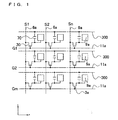
- Fig. 1 is an equivalent circuit of various elements, wiring lines, etc. in a plurality of pixels formed in a matrix that constitutes an image display region of the electro-optical device.
- Figs. 2 and 3 are plan views of a plurality of pixel groups adjacent to each other on a TFT array substrate on which data lines, scanning lines, and pixel electrodes are formed.
- Figs. 2 and 3 respectively illustrate a lower portion (Fig. 2) and an upper portion (Fig. 3) in a laminated structure to be described later.
- Fig. 4 is a sectional view taken along the line A-A' in the case where Figs. 2 and 3 overlap. In Fig. 4, the contraction scales of each layer and member are different to make each layer and member recognizable in the figure.
- pixel electrodes 9a and TFTs 30 for switching and controlling the pixel electrodes 9a are formed in a plurality of pixels in a matrix that constitutes an image display region of an electro-optical device according to the present embodiment.
- Data lines 6a to which image signals are supplied are electrically connected to the sources of the TFTs 30.
- the image signals S1, S2,..., and Sn written in the data lines 6a may be line-sequentially supplied in this order and may be supplied to respective groups each being composed of a plurality of adjacent data lines 6a.
- Gate electrodes 3a are electrically connected to the gates of the TFTs 30. At a predetermined timing, scanning signals G1, G2,..., and Gm are line-sequentially applied to scanning lines 11a and the gate electrodes 3a as pulses in this order.
- the pixel electrodes 9a are electrically connected to the drains of the TFTs 30, and the switches of the TFTs 30, which are switching elements, are closed for a certain period of time, such that the image signals S1, S2,..., and Sn supplied from the data lines 6a are written at a predetermined timing.
- the image signals S1, S2,..., and Sn of a predetermined level that are written in liquid crystal, an example of an electro-optical material, through the pixel electrodes 9a are stored between counter electrodes formed on a counter substrate for a certain period.
- the alignment or order of the molecules of the liquid crystal changes according to the level of an applied voltage, such that light is modulated to thus display a grayscale.
- a normally white mode the transmittance of incident light decreases in accordance with the voltage applied to each pixel unit.
- a normally black mode the transmittance of the incident light increases in accordance with the voltage applied to each pixel unit.
- light having contrast in accordance with the image signals is emitted from the electro-optical device.
- storage capacitors 70 are added in parallel to the liquid crystal capacitors formed between the pixel electrodes 9a and the counter electrodes.
- the storage capacitors 70 are provided in the regions of the scanning lines 11a and the data lines 6a and include fixed-electric-potential-side capacitor electrodes and the capacitor electrodes 300 fixed to the electrostatic potential.
- the plurality of pixel electrodes 9a are provided on a TFT array substrate 10 in a matrix (the contours are marked with dotted lines) and the data lines 6a and the scanning lines 11a are provided along the vertical and horizontal boundaries of the pixel electrodes 9a.
- the data lines 6a have a laminated structure including aluminum, to be described later.
- the scanning lines 11a are made of, for example, a conductive polysilicon film, etc.
- the scanning lines 11a are electrically connected to the gate electrodes 3a that face channel regions 1a' in the regions marked with upward-leaning oblique lines in semiconductor layers 1a through contact holes 12cv.
- the gate electrodes 3a are included in the scanning lines 11a.
- the electro-optical device comprises the TFT array substrate 10 made of a quartz substrate, a glass substrate, a silicon substrate, etc. and a counter substrate 20 made of a glass substrate or a quartz substrate, which faces the TFT array substrate 10.
- the pixel electrodes 9a are provided on the side of the TFT array substrate 10, as illustrated in Fig. 4, the pixel electrodes 9a are provided.
- the pixel electrodes 9a are made of, for example, a transparent conductive film such as an indium tin oxide (ITO) film.
- ITO indium tin oxide
- counter electrodes 21 are provided over the entire surface.
- An alignment film 22 on which a predetermined alignment process such as a rubbing process is performed is provided under the counter electrodes 21.
- the counter electrodes 21 are made of a transparent conductive film such as an ITO film, like the above-described pixel electrodes 9a.
- An electro-optical material such as liquid crystal is filled in a space surrounded by a sealing material 52 (refer to Figs. 17 and 18), to be described later, between the TFT array substrate 10 and the counter substrate 20 that face each other, to form a liquid crystal layer 50.
- the liquid crystal layer 50 is given a predetermined alignment state by the alignment films 16 and 22 when an electric field is not applied from the pixel electrodes 9a.
- the laminated structure is composed of a first layer including the scanning lines 11a, a second layer including the TFTs 30 that include the gate electrodes 3a, a third layer including the storage capacitors 70, a fourth layer including data lines 6a, a fifth layer including capacitor wiring lines 40, and a sixth layer (the uppermost layer) including the pixel electrodes 9a and the alignment film 16, in order from the bottom.
- An underlying insulating film 12 is provided between the first layer and the second layer.
- a first interlayer insulating film 41 is provided between the second layer and the third layer.
- a second interlayer insulating film 42 is provided between the third layer and the fourth layer.
- a third interlayer insulating film 43 is provided between the fourth layer and the fifth layer.
- a fourth interlayer insulating film 44 is provided between the fifth layer and the sixth layer.
- scanning lines 11a are provided in the first layer.
- the scanning lines 11a are made of elemental metal, an alloy, metal silicide, polysilicide including at least one high-melting-point metal such as Ti, Cr, W, Ta, and Mo, and a laminate thereof, or conductive polysilicon.
- the scanning lines 11a are patterned in stripes in plan view in the direction X of Fig. 2.
- the scanning lines 11a in stripes include main line portions that extend in the X-direction of Fig. 2, and protrusion portions that extend in the Y-direction of Fig. 2 to which the data lines 6a or the capacitor wiring lines 400 extend.
- the protrusion portions that extend from the adjacent scanning lines 11a are not connected to each other. Thus, each of the scanning lines 11a is isolated.
- the TFTs 30 including the gate electrodes 3a are provided as the second layer.
- the TFTs 30 have a lightly doped drain (LDD) structure and include the above-described gate electrodes 3a, the channel regions 1a' of the semiconductor layers 1a, which are made of a polysilicon film and which have channels formed by the electric field from the gate electrodes 3a, insulating films 2 including a gate insulating film for insulating the gate electrodes 3a from the semiconductor layers 1a, and lightly doped source regions 1b, lightly doped drain regions 1c, heavily doped source regions 1d, and heavily doped drain regions 1e in the semiconductor layers 1a.
- LDD lightly doped drain
- relay electrodes 719 are formed on the second layer using the same film as the gate electrodes 3a. As illustrated in Fig. 2, each of the relay electrodes 719 is formed like an island in plan view, to be positioned almost in the center of a side that extends in the X-direction of each of the pixel electrodes 9a. Since the relay electrodes 719 and the gate electrodes 3a are made of the same film, for example, when the gate electrodes 3a are made of the conductive polysilicon film, the relay electrodes 719 are also made of the conductive polysilicon film.
- the above-described TFTs 30 preferably have the LDD structure: however, they may have an offset structure in which impurities are not implanted into the lightly doped source regions 1b and the lightly doped drain regions 1c.
- Self-aligned-type TFTs having heavily doped source regions and heavily doped drain regions formed by self-matching by implanting impurities with high concentration using the gate electrodes 3a as a mask may be used.
- the underlying insulating film 12 made of the silicon oxide film, etc. is provided on the scanning lines 11a and under the TFTs 30.
- the underlying insulating film 12 interlayer-insulates the TFTs 30 from the scanning lines 11a.
- the underlying insulating film 12 formed on the entire surface of the TFT array substrate 10 prevents the characteristics of the pixel switching TFTs 30 from changing due to the roughness caused by the process of abrading the surface of the TFT array substrate 10, and the dirt that remains after cleaning the TFT array substrate 10.
- Contact holes 12cv are formed in the underlying insulating film 12 at both sides of the semiconductor layers 1a, in plan view, in the direction of the channel length of the semiconductor layers 1a that extend along the data lines 6a, to be described later.
- concave portions are formed under the gate electrodes 3a laminated above the contact holes 12cv.
- the gate electrodes 3a are formed to cover the entire region of the contact holes 12cv, such that sidewall portions 3b (the above-described concave portions) integrated with the gate electrodes 3a are provided in the gate electrodes 3a.
- the semiconductor layers 1a of the TFTs 30 are covered from the side in plan view, such that it is possible to prevent light from being incident on the covered portions or reduce the amount of such incident light.
- the sidewall portions 3b are formed to cover the contact holes 12cv, and the lower ends thereof are connected to the scanning lines 11a.
- the scanning lines 11a are formed in stripes, as described above, such that the gate electrode 3a and the scanning line 11a in a certain row always have the same electric potential in the row.
- the storage capacitors 70 are provided.
- the storage capacitors 70 are formed such that lower electrodes 71, serving as pixel-electric-potential-side capacitor electrodes and being connected to the heavily doped drain regions 1e and the pixel electrodes 9a of the TFTs 30, face the capacitor electrodes 300, serving as fixed-electric-potential-side capacitor electrodes, with dielectric films 75 interposed therebetween.
- the storage capacitors 70 it is possible to significantly improve the potential storage characteristics of the pixel electrodes 9a.
- the storage capacitors 70 according to the present embodiment do not reach light transmission regions almost corresponding to the regions in which the pixel electrodes 9a are formed.
- the storage capacitors 70 are accommodated in light shielding regions, the pixel-aperture ratio of the entire electro-optical device remains large, such that it is possible to display brighter images . Since the storage capacitors 70 are especially important in the present invention, the storage capacitors 70 will be described in more detail later in the sections "Structure of Storage Capacitors” and “Method of Manufacturing Storage Capacitors”.
- a silicate glass film such as NSG (Non Silicate Glass), PSG (Phosphorus Silicate Glass), BSG (Boron Silicate Glass), BPSG (Boron Phosphorus Silicate Glass), etc.
- a silicon nitride film, or a silicon oxide film, or preferably NSG is formed on the TFTs 30 or the gate electrodes 3a, on the relay electrodes 719, and under the storage capacitors 70.
- contact holes 81 for electrically connecting the heavily doped source regions 1d of the TFTs 30 to the data lines 6a, to be described later, are provided to pass through the second interlayer insulating film 42, to be described later.
- contact holes 83 for electrically connecting the heavily doped drain regions 1e of the TFTs 30 to the lower electrodes 71 that constitute the storage capacitors 70 are formed as open holes.
- contact holes 881 for electrically connecting the lower electrodes 71, serving as the pixel-electric-potential-side capacitor electrodes that constitute the storage capacitors 70, to the relay electrodes 719 are provided.
- contact holes 882 for electrically connecting the relay electrodes 719 to the second relay electrodes 6a2, to be described later are provided as open holes to pass through the second interlayer insulating film, to be described later.
- the data lines 6a are provided.
- the data lines 6a have a three-layered structure, such as a layer made of aluminum (refer to the reference numeral 41A in Fig. 4), a layer made of titanium nitride (refer to the reference numeral 41TN in Fig. 4), and a layer made of silicon nitride (refer to the reference numeral 401 in Fig. 4) in order from the bottom.
- the silicon nitride film is patterned with a little large size to cover the aluminum layer and the titan nitride layer thereunder.
- capacitor wiring line relay layers 6a1 and the second relay electrodes 6a2 are formed of the same film as the data lines 6a. As illustrated in Fig. 3, they are not continuous to the data lines 6a on a plane but are isolated from each other after being patterned in plan view. For example, when attention is paid to the data line 6a positioned on the leftmost side in Fig. 3, the almost quadrangular capacitor wiring line relay layers 6a1 and the almost quadrangular second relay electrode 6a2 whose area is slightly larger than that of the capacitor wiring line relay layer 6a1 are formed on the right side of the data line 6a.
- capacitor wiring line relay layers 6a1 and the second relay electrodes 6a2 are formed of the same film as the data lines 6a, they have a three-layered structure such as the layer made of aluminum, the layer made of titan nitride, and the layer made of plasma nitride film, in order from the bottom.
- the second interlayer insulating film 42 formed of the silicate glass film such as NSG, PSG, BSG, and BPSG, the silicon nitride film or the silicon oxide film, or preferably formed by a chemical vapor deposition (CVD) method using TEOS gas is provided on the storage capacitors 70 and under the data lines 6a.
- the contact holes 81 for electrically connecting the heavily doped source regions 1d of the TFTs 30 to the data lines 6a and contact holes 801 for electrically connecting the capacitor wiring line relay layers 6a1 to the capacitor electrodes 300 that are the upper electrodes of the storage capacitors 70 are provided.
- the contact holes 882 for electrically connecting the second relay electrodes 6a2 to the relay electrodes 719 are formed.
- capacitor wiring lines 400 are formed. As illustrated in Fig. 3, the capacitor wiring lines 400 are formed in a matrix to extend in the X and Y-directions in the drawing in plan view. Among the capacitor wiring lines 400, the portions that extend in the Y-direction in the drawing are particularly wider than the data lines 6a in order to cover the data lines 6a. Also, each of the portions that extend in the X-direction in the drawing has a notch in the center of one side of each of the pixel electrodes 9a in order to secure regions in which the third relay electrodes 402 are formed.
- the capacitor wiring lines 400 extend from the image display region 10a in which the pixel electrodes 9a are arranged to the vicinity thereof to be electrically connected to an electrostatic potential source and to have fixed electric potential.
- the third relay electrodes 402 are formed of the same film as the capacitor wiring lines 400.
- the third relay electrodes 402 relay electrical connection between the second relay electrodes 6a2 and the pixel electrodes 9a through contact holes 804 and 89, to be described later.
- the capacitor wiring lines 400 and the third relay electrodes 402 are not continuous with each other on a plane but are isolated from each other after being patterned.
- the capacitor wiring lines 400 and the third relay electrodes 402 have a two-layered structure, such as the layer made of aluminum as a lower layer and the layer made of titanium nitride as an upper layer.
- the third interlayer insulating film 43 is formed on the data lines 6a and under the capacitor wiring lines 400.
- contact holes 803 for electrically connecting the capacitor wiring lines 400 to the capacitor wiring line relay layers 6a1 and contact holes 804 for electrically connecting the third relay electrodes 402 to the second relay electrodes 6a2 are formed as open holes.
- the pixel electrodes 9a are formed in a matrix.
- the alignment film 16 is formed on the pixel electrodes 9a.
- the fourth interlayer insulating film 44 is formed under the pixel electrodes 9a.
- contact holes 89 for electrically connecting the pixel electrodes 9a to the third relay electrodes 402 are formed as open holes.
- the pixel electrodes 9a and the TFTs 30 are electrically connected to each other through the contact holes 89, the third relay layer 402, the contact holes 804, the second relay layers 6a2, the contact holes 882, the relay electrodes 719, the contact holes 881, the lower electrodes 71, and the contact holes 83.
- Fig. 5 is an enlarged sectional view illustrating the vicinity of the end part of the storage capacitor 70 in the circle denoted by the reference numeral C of Fig. 4.
- Fig. 6 is an enlarged sectional view illustrating the portion denoted by the reference numeral 300C of Fig. 5.
- Fig. 5 is an enlarged sectional view illustrating the vicinity of the end part of the storage capacitor 70 in the circle denoted by the reference numeral C of Fig. 4.
- Fig. 6 is an enlarged sectional view illustrating the portion denoted by the reference numeral 300C of Fig. 5.
- Fig. 5 is an enlarged sectional view illustrating the vicinity of the end part of the storage capacitor 70 in the circle denoted by the reference numeral C of Fig. 4.
- Fig. 6 is an enlarged sectional view illustrating the portion denoted by the reference numeral 300C of Fig. 5.
- Fig. 5 is an enlarged sectional view illustrating the vicinity of the end part of the storage capacitor 70 in the circle denote
- the storage capacitors 70 comprise the lower electrodes 71, the capacitor electrodes 300, and the dielectric films 75.
- the lower electrodes 71 are made of the conductive polysilicon film and function as the pixel-electric-potential-side capacitor electrodes.
- the lower electrodes 71 have the function of relay-connecting the pixel electrodes 9a to the heavily doped drain regions 1e of the TFTs 30, as well as the function of the pixel-electric-potential-side capacitor electrodes.
- the relay connection described herein is performed through the relay electrodes 719.
- the capacitor electrodes 300 are made of the conductive polysilicon film, and function as the fixed-electric-potential-side capacitor electrodes of the storage capacitors 70. According to the present embodiment, in order to make the capacitor electrodes 300 have the fixed electric potential, the capacitor electrodes 300 must be electrically connected to the capacitor wiring lines 400 having the fixed electric potential.
- the dielectric films 75 are composed of silicon oxide film having a thickness of about 5 to 200 nm, such as a HTO (High Temperature Oxide) film and a LTO (Low Temperature Oxide) film.
- the dielectric films 75 are preferably thinner as long as it is possible to achieve sufficient reliability.
- the dielectric films 75 have a single-layered structure.
- the dielectric films 75 may have a two-layered structure, such as a silicon nitride film and a silicon oxide film, or a structure with three or more layers.
- the capacitor electrodes 300, the lower electrodes 71, and the dielectric films 75 are formed to have the same shape in plan view.
- the end face 300W of the capacitor electrode 300 and the end face 71W of the lower electrode 71 are placed on an imaginary plane (not shown) perpendicularly to the TFT array substrate 10.
- the end faces 300W and 71W are aligned as illustrated in Figs. 5 and 6.
- capacitor electrodes 300 and both relay electrodes 71 face each other, it is possible to address or achieve reduction and minuteness in size of the electro-optical device and to prevent the capacitance of the storage capacitors from being undesirably reduced or lower the amount this capacitance is reduced.
- the surfaces of the capacitor electrode 300 and the lower electrode 71 are oxidized as illustrated in Figs. 5 and 6 (not shown in Fig. 4) to thus form oxidation films 501.
- the oxidation films 501 are formed on the top and bottom surfaces of the capacitor electrode 300 as well as on the end face 300W of the capacitor electrode 300.
- the oxidation films 501 are formed on the top and bottom surfaces of the lower electrode 71 as well as on the end face 71W of the lower electrode 71.
- the bottom surface of the capacitor electrode 300 is oxidized because oxygen is supplied to the bottom surface of the capacitor electrode 300 through the dielectric film 75.
- the bottom surface of the lower electrode 71 is oxidized because oxygen is supplied to the bottom surface of the lower electrode 71 through the first interlayer insulating film 41.
- the oxidation film 501 at the edge portion 300C included in the end face 300W, as illustrated in Fig. 6, (1/2) of an almost semi-circular region ((1/8) of an almost semi-spherical region based on the edge in three dimensions) is the oxidation film 501.
- the thickness of the oxidation film 501 at the edge portion 300C is larger than that in the other portions.
- the thickness of the oxidation film 501 at the edge portion 300C refers to the portion denoted by the reference numeral Dc illustrated in Fig. 6.
- the thickness Dc of the oxidation film 501 at the edge 300C satisfies the condition 1.5 [nm] ⁇ D ⁇ 30 [nm].
- the electro-optical device includes such oxidation films 501 to thus obtain the following effects. That is, it is possible to prevent the capacitor electrodes 300 and the lower electrodes 71 from being short circuited due to the oxidation films 501 or reduce the frequency with which this happens. In particular, since the oxidation films 501 are also formed on the end faces 300W and 71W and the edge portions 300C and 71C, it is possible to significantly improve the breakdown-voltage performance of the storage capacitors 70.
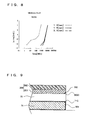
- Fig. 7 is a graph illustrating the breakdown-voltage performance of the storage capacitor 70 when the oxidation film 501 is included, and the breakdown-voltage performance of the storage capacitor 70 when the oxidation film 501 is not included. More specifically, Fig. 7 is a weibull plot illustrating, when a uniform voltage 18.5 [V] is continuously applied to the storage capacitor 70 (see the reference numeral Q2 in the drawing) with the oxidation film 501 and to the storage capacitor (see the reference numeral Q1 in the drawing) without the oxidation film 501, how the failure rate of the storage capacitor increases.
- the horizontal axis of Fig. 7 represents time t and the vertical axis of Fig.
- FIG. 7 represents In(-In(1-F(t))) expressed by a failure distribution function (an unreliability function) F(t).
- the breakdown-voltage performance of the storage capacitor 70 (see the reference numeral Q2) with the oxidation film 501 is better than the breakdown-voltage performance of the storage capacitor (see the reference numeral Q1) without the oxidation film 501 considering that, with respect to the storage capacitor 70 with the oxidation film 501, the graph starts at a time later than the time at which the graph starts with respect to the storage capacitor without the oxidation film 501.
- the oxidation films 501 are formed on the capacitor electrodes 300 and the lower electrodes 71 that constitute the storage capacitors 70, the breakdown-voltage performance of the storage capacitors 70 improves. Therefore, since the storage capacitors 70 according to the present embodiment can sufficiently display the expected performance of improving the potential storage characteristic of the pixel electrodes 9a, it is possible to provide an electro-optical device capable of displaying high quality images and of more stably operating.
- Fig. 8 is a graph illustrating the influence of the thickness of the oxidation film on the improvement of the breakdown-voltage performance of the storage capacitor.
- Fig. 8 is a weibull plot obtained when a uniform voltage of 18.5 [V] is continuously applied to the storage capacitor 70, like in Fig. 7, in which the thickness D of the oxidation film 501 is changed as a parameter (1, 1.5, and 3 [nm]).
- a remarkable difference exists between the case in which the thickness D of the oxidation film 501 is 1 [nm] and the cases in which the thickness D of the oxidation film 501 is 1.5 [nm] and 2 [nm]. That is, whereas the graph starts at a relatively early stage in the former, the graph starts at a relatively late state in the latter.
- the increase and decrease of the thickness D of the oxidation film 501 greatly affects the improvement of the breakdown-voltage performance of the storage capacitor 70 between the case in which the thickness D is 1 [nm] and the case in which the thickness D is 1.5 [nm].
- the thickness D of the oxidation film 501 is greater than 1.5 [nm]
- the improvement of the breakdown-voltage performance of the storage capacitor 70 remains stable thereafter.
- the thickness D of the oxidation film 501 is preferably no less than 1.5 [nm].
- the thickness D of the oxidation film 501 is preferably as large as possible. That is, when the thickness D of the oxidation film 501 is too large, in the thermal oxidation process of forming the oxidation film 501, the semiconductor layer 1a of the TFT 30 is also oxidized to thus decrease the switching ON current of the TFT 30.
- the thickness D of the oxidation film 501 is preferably no more than a certain level, more specifically, no more than 30 [nm].
- the thickness D of the oxidation film 501 satisfies the condition 1.5 [nm] ⁇ T ⁇ 30 [nm]
- the portions that mainly control the breakdown-voltage performance of the storage capacitor 70 are the edge portions 300C and 71C, it is assumed that it is possible to obtain the above-described effects when oxidation films are sufficiently formed on those portions.
- the condition 1.5 [nm] ⁇ D ⁇ 30 [nm] can be changed to 1.5 [nm] ⁇ Dc ⁇ 30 [nm], if necessary.
- the oxidation process can be performed only on the edge portions 300C and 71C to satisfy the condition related to the thickness Dc (see Figs. 9, 10, and 12).
- Such a form is also within the scope of the present invention.
- Figs. 9 and 10 are sectional views illustrating storage capacitors having capacitor electrodes according to aspects different from the aspect of Fig. 5 but with the same purpose as Fig. 5.
- Fig. 11 is a sectional view illustrating a storage capacitor having a lower electrode according to an aspect different from the aspect of Fig. 5 but with the same purpose as Fig. 5.
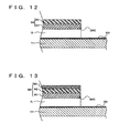
- Figs. 12 and 13 are sectional views illustrating storage capacitors having capacitor electrodes according to aspects different from the aspect of Fig. 11 but with the same purpose as Fig. 11.
- the silicon nitride film may be used instead of or in addition to the silicon oxide film ("in addition” means that the dielectric film 75 may have the two-layered structure such as the silicon oxide film and the silicon nitride film as described above).
- the dielectric film 75 includes the silicon nitride film having a relatively large dielectric constant, so that it is possible to increase the capacitance of the storage capacitor 70.
- the dielectric films 75 include silicon nitride film, the breakdown-voltage performance of the storage capacitors 70 is hardly decreased even if the thickness of the dielectric film 75 is reduced as small as possible.
- tungsten silicide may be used instead of the conductive polysilicon film or in addition to the conductive polysilicon film, as illustrated in Fig. 9.
- a capacitor electrode 350 has a conductive polysilicon film 351 thereunder and a WSi film 352 thereon.
- the capacitor electrode 350 is arranged to cover the semiconductor layer 1a (see Figs. 2 and 3), and includes the WSi film 352 having a relatively excellent light absorbing performance to thus prevent light from being incident on the semiconductor layer 1a or the channel region 1a' thereof or reduce the amount of such incident light. That is, the generation of light leakage current in the semiconductor layer 1a can be reduced or prevented.
- the storage capacitor 70 functions as a light shielding film and also has an excellent breakdown-voltage performance, so that it is possible to realize two functions by one structure. As a result, it is possible to simplify the structure of the electro-optical device, and to address or achieve reduction and minuteness in size of the electro-optical device.
- the WSi film 352 when the thermal oxidation process is performed in order to obtain the oxidation film 502, or the oxidation film 501 in the lower electrode 71, the WSi film 352 may be significantly oxidized.
- a silicon nitride film 363 may be provided on the WSi film 362 in addition to the conductive polysilicon film 361 and the WSi film 362. It is possible to prevent the WSi film 362 from being oxidized due to the presence of the silicon nitride film 363.
- CoSi and TiSi as well as WSi are used as a material for effectively shielding the semiconductor layers 1a from light.
- elemental metal, an alloy, metal silicide, polysilicide including at least one high-melting-point metal such as Ti, Cr, W, Ta, and Mo, and a laminate thereof may be used.
- the lower electrodes 71 as well as the capacitor electrodes 300 may adopt the same structure described above with respect to the capacitor electrodes 300, or may be formed of a single-layered film or a multi-layered film including metal or an alloy.
- the shapes of the capacitor electrode 300 and the lower electrode 71 are the same in plan view.
- the present invention is not limited to this embodiment. For example, as illustrated in Fig.
- the storage capacitor may be formed such that the area of a lower electrode 711 on the lower layer can be larger and that the area of the capacitor electrode 300 on the upper layer can be smaller. Even in this case, as long as the end face 300W or the edge portion 300C of the capacitor electrode 300 exists, defects such as damage of the insulation property caused by electrostatic focusing are generated at the edge portion 300C.
- the oxidation film 501 is formed on the capacitor electrode 300 like in Fig. 5, and the oxidation film 503 is formed on the lower electrode 711. Therefore, the breakdown-voltage performance of the storage capacitor is improved. According to the structure related to Fig. 11, as illustrated in Figs.
- the storage capacitor may be formed with the same purpose as those illustrated in Figs. 9 and 10.
- the oxidation film in Figs. 12 and 13 is formed only on the edge portion 350C of the capacitor electrode 350 and the edge portion 360C of the capacitor electrode 360.
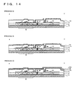
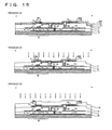
- Figs. 14 and 15 are sectional views illustrating, in order, the manufacturing processes of the electro-optical device according to the present embodiment shown in Fig. 4.
- the manufacturing processes of the storage capacitor 70 particularly related to the present invention will only be described.
- Figs. 14 and 15 the structure on the side of the counter substrate 20 is omitted.
- an amorphous silicon film is formed on the first interlayer insulating film 41 in a low temperature atmosphere of about 450°C to 550°C, preferably about 500°C, by a low pressure CVD method (for example, a CVD method with a pressure of about 20 to 40 Pa) using monosilane gas and disilane gas with a flow rate of about 400 to 600 cc/min.
- a low pressure CVD method for example, a CVD method with a pressure of about 20 to 40 Pa
- monosilane gas and disilane gas with a flow rate of about 400 to 600 cc/min.
- P (Phosphorus) ions are introduced into the atmosphere, such that the amorphous silicon film is doped with the P ions.
- a thermal process is performed in a nitrogen atmosphere at a temperature of about 600 to 700°C for about 1 to 10 hours, preferably for 4 to 6 hours, such that a p-Si (polysilicon) film is solid-phase grown to a thickness of about 50 to 200 nm, preferably about 100 nm.
- a firing process using rapid thermal anneal (RTA) or a laser firing process using an excimer laser may be used.
- the polysilicon film corresponds to a precursor film 71K which will become the lower electrode 71.
- a precursor film 75K of the dielectric film 75 is formed on the precursor film 71K.
- the precursor film 75K is thermally oxidized at a temperature of 900 to 1300°C, preferably about 1,000°C, to thus form a lower insulating film. Then, if necessary, an upper insulating film is formed by a low pressure CVD method, such that a single-layered or a multi-layered high-temperature silicon oxide film (a HTO film) or silicon nitride film is formed. Next, as illustrated in process (3) of Fig. 14, a precursor film 300K which will become the capacitor electrode 300 is formed like the precursor film 71K.
- the precursor film 71K, the precursor film 75K, and the precursor film 300K are simultaneously patterned (by photolithography and etching).
- the storage capacitors 70 comprising the lower electrode 71 obtained by patterning the precursor film 71K, the dielectric film 75 obtained by patterning the precursor film 75K, and the capacitor electrode 300 obtained by patterning the precursor film 300K, are formed.
- the precursor film 71K, the precursor film 75K, and the precursor film 300K are simultaneously patterned, it is possible to simplify the manufacturing processes compared to the case in which the capacitor electrode 300, the dielectric film 75, and the lower electrode 71 are formed separately.
- the end face 300W of the capacitor electrode 300, the end face 75W of the dielectric film 75, and the end face 71W of the lower electrode 71 are placed on the same plane.
- the capacitor electrode 300, the lower electrode 71, and the dielectric film 75 are patterned to have the same planar shape in plan view.
- the surfaces of the capacitor electrode 300 and the lower electrode 71 formed as described above are preferably oxidized by a thermal oxidation process (see Figs. 5 and 6). More specifically, for example, the surfaces of the capacitor electrode 300 and the lower electrode 71 are thermally oxidized in a longitudinal-type thermal diffusion furnace in an atmosphere where the concentration of oxygen (O 2 ) is 2% at a temperature of 850 [°C] for 5 minutes.
- the concentration of oxygen (O 2 ) is 2% at a temperature of 850 [°C] for 5 minutes.
- the oxidation film 501 that satisfies the condition 1.5 [nm] ⁇ D ⁇ 30 [nm], wherein D is the thickness of the oxidation film.
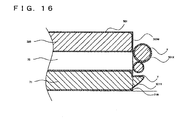
- arrows schematically illustrate that the oxidation process is performed.
- a remnant X may reside around the end face 300W or the end face 71W by performing an etching process during the patterning process.
- the remnant X in Fig. 16 and a remnant Y, to be described later, are exaggerated for clarity.
- the remnant X remains, according to the present embodiment, in particular, since the end faces 300W and 71 W exist, the breakdown-voltage performance of the capacitor electrode 300 and the lower electrode 71 deteriorates and, in some cases, the capacitor electrode 300 and the lower electrode 71 may be short circuited. As illustrated in Fig.
- the thermal oxidation process is performed as described above.
- the remnants X and Y are oxidized as illustrated in Fig. 16, so that oxidation films 501X and 501Y are formed on the surfaces of remnants X and Y.
- the oxygen concentration and oxidation temperature are determined to satisfy the following conditions.
- the oxygen concentration is preferably no less than 2 [%].
- the oxidation temperature is preferably no less than 350 [°C].
- the atmosphere temperature is preferably as high as possible since the atmosphere temperature significantly contributes to the speed at which the oxidation film 501 is formed.
- the oxidation temperature is preferably no less than 800 [°C], and more preferably about 850 [°C], as described above.
- the storage capacitor 70 according to the present embodiment composed of the capacitor electrode 300 and the lower electrode 71 including the oxidation films 501 is completed.
- the following manufacturing method can be adopted. That is, according to the above-described manufacturing method, after patterning the precursor film 300K, etc., the thermal oxidation process is immediately performed.
- the thermal oxidation process instead of this, for example, as illustrated in process (6) of Fig. 15, after performing the patterning process to thus form the storage capacitor 70, and forming the second interlayer insulating film 42 on the storage capacitor 70, the thermal oxidation process may be performed. In this case, the thermal oxidation is not performed in process (5). Thus, it is considered that the arrows do not exist in process (5).
- the thermal oxidation is preferably performed in the longitudinal-type thermal diffusion furnace in an atmosphere where the oxygen concentration is 2% at a temperature of 950 [°C] for 20 minutes.
- the processes are preferably performed in an atmosphere where a proper amount of oxygen gas that satisfies the above-described oxygen concentration is added to nitrogen gas.
- the thermal oxidation process may be performed after forming the second interlayer insulating film 42 and, furthermore, after forming the data lines 6a, the capacitor wiring line relay electrodes 6a1, and the second relay electrodes 6a2.
- the thermal oxidation process is performed at a temperature no more than the lowest melting point ("of the layer 41A made of aluminum" in the present embodiment) among the melting points of the respective layers that constitute the data lines 6a.
- the thermal oxidation process is performed at a temperature no more than the lowest melting point ("of the layer 41A made of aluminum" in the present embodiment) among the melting points of the respective layers that constitute the data lines 6a.
- the thermal oxidation process may be performed at any point of time after forming the data lines 6a, that is, after forming the third interlayer insulating film on the data lines 6a and, furthermore, after forming the capacitor wiring lines 400 on the third interlayer insulating film 43.
- the melting points of the data lines 6a, the capacitor wiring lines 400, and the pixel electrodes 9a matter. It is needless to mention that it is necessary to consider the oxidation temperature as described above so that the respective components are not melted.
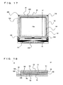
- Fig. 17 is a plan view of the electro-optical device, in which the TFT array substrate, together with the respective components formed on the TFT array substrate, is seen from the counter substrate.
- Fig. 18 is a sectional view taken along the line H-H' of Fig. 17.
- a liquid crystal device with a built-in driving circuit TFT active-matrix-driving mode which is one example of the electro-optical device, is taken as an example.
- the TFT array substrate 10 and the counter substrate 20 are arranged to face each other.
- the liquid crystal layer 50 is sealed between the TFT array substrate 10 and the counter substrate 20.
- the TFT array substrate 10 and the counter substrate 20 are attached to each other by the sealing material 52 provided in the sealing region around the image display region 10a.
- the sealing material 52 for attaching the two substrates to each other is made of UV-curable resin or thermo-setting resin.
- the sealing material 52 is hardened by radiating UV rays thereonto and heating the TFT array substrate 10, after being coated into the TFT array substrate 10 in the manufacturing processes.
- Gap materials such as glass fibers or glass beads for making the TFT array substrate 10 and the counter substrate 20 separated from each other by a predetermined distance (a gap between the TFT array substrate 10 and the counter substrate 20) are scattered in the sealing material 52.
- the electro-optical device according to the present invention is used for a light valve of a projector and is suitable for displaying small and enlarged images.
- a frame-shaped light shielding film 53 that defines the frame region of the image display region 10a is provided at the side of the counter substrate 20 together with the sealing material 52 which is arranged inside the sealing region. Part or all of the frame-shaped light shielding film 53 may be provided at the side of the TFT array substrate 10 as a built-in light shielding film.
- a data line-driving circuit 101 and external circuit connection terminals 102 are provided along one side of the TFT array substrate 10.
- Scanning line-driving circuits 104 are provided along two sides adjacent to the one side to be covered with the frame-shaped light shielding film 53.
- a plurality of wiring lines 105 are provided along the remaining one side of the TFT array substrate 10 to be covered with the frame-shaped light shielding film 53 in order to connect the two scanning line-driving circuits 104 provided on both sides of the image display region 10a.
- Upper and lower connecting materials 106 that function as upper and lower connecting terminals between the two substrates are arranged at four corners of the counter substrate 20.
- the upper and lower connecting terminals are provided in the TFT array substrate 10 in the regions facing the corners.
- the TFT array substrate 10 and the counter substrate 20 can be electrically connected to each other.
- an alignment film is formed on the pixel electrodes 9a after the wiring lines such as the pixel switching TFTs, the scanning lines, and the data lines are formed.
- a light shielding film 23 in a matrix or in strips, and an alignment film on the uppermost layer are formed on the counter substrate 20, other than the counter electrodes 21, a light shielding film 23 in a matrix or in strips, and an alignment film on the uppermost layer are formed.
- the liquid crystal layer 50 is made of, for example, liquid crystal obtained by mixing one kind or various kinds of nematic liquid crystal and has a predetermined alignment state between the pair of alignment films.
- sampling circuits for sampling image signals on image signal lines to thus supply the image signals to the data lines in addition to the data line driving circuit 101 and the scanning line driving circuits 104, sampling circuits for sampling image signals on image signal lines to thus supply the image signals to the data lines, precharge circuits for supplying precharge signals of a predetermined voltage level to the plurality of data lines prior to the image signals, and test circuits for testing the quality and defects of the electro-optical device during the manufacturing or on shipping may be formed.
- Fig. 19 is a schematic sectional view of the projection-type color display device.
- a liquid crystal projector 1100 which is an example of the projection-type color display device according to the present embodiment, has three liquid crystal modules each including a liquid crystal device in which a driving circuit is mounted on a TFT array substrate.
- the liquid crystal modules are used as RGB light valves 100R, 100G, and 100B.
- the above-described electro-optical device (refer to Figs. 1 to 5) is used as the light valves 100R, 100G, and 100B.
- the liquid crystal projector 1100 when projection light is emitted from a lamp unit 1102 that is a white light source, such as a metal halide lamp, the emitted light is divided into light components R, G, and B corresponding to the three primary colors RGB, by three mirrors 1106 and two dichroic mirrors 1108, and the light components R, G, and B are guided by the light valves 100R, 100G, and 100B corresponding to the respective colors.
- the light component B is guided by a relay lens system 1121 composed of an incidence lens 1122, a relay lens 1123, and an emission lens 1124 in order to prevent optical loss from occurring due to the long light path.
- the light components corresponding to the three primary colors modulated by the light valves 100R, 100G, and 100B are combined by a dichroic prism 1112 again and the combined light is projected onto a screen 1120 through a projection lens 1114 as a color image.
Landscapes
- Physics & Mathematics (AREA)
- Nonlinear Science (AREA)
- Engineering & Computer Science (AREA)
- Crystallography & Structural Chemistry (AREA)
- Mathematical Physics (AREA)
- Chemical & Material Sciences (AREA)
- Microelectronics & Electronic Packaging (AREA)
- General Physics & Mathematics (AREA)
- Optics & Photonics (AREA)
- Power Engineering (AREA)
- Liquid Crystal (AREA)
- Devices For Indicating Variable Information By Combining Individual Elements (AREA)
- Thin Film Transistor (AREA)
- Electroluminescent Light Sources (AREA)
- Electrochromic Elements, Electrophoresis, Or Variable Reflection Or Absorption Elements (AREA)
Abstract
Description
The electro-optical device further comprises a counter substrate that faces the substrate, counter electrodes that face the pixel electrodes on the counter substrate, and a liquid crystal layer interposed between the pixel electrodes and the counter electrodes to thus display images. That is, the alignment of liquid crystal molecules in the liquid crystal layer properly changes according to a predetermined potential difference between the pixel electrodes and the counter electrodes, such that the transmittance of light that passes through the liquid crystal layer changes to display images.
However, the electro-optical device according to the conventional technology has the following problems. That is, the storage capacitors typically have a three-layered structure including first electrodes electrically connected to the TFTs and the pixel electrodes, second electrodes that face the first electrodes and that have fixed electric potential, and dielectric films interposed between both electrodes. Here, the first and second electrodes must not be electrically connected: if the first electrodes and the second electrodes are short circuited, the storage capacitors cannot function properly.
Recently, it is also necessary that electro-optical devices be made smaller in size, and for various components, such as TFTs, data lines, scanning lines, and pixel electrodes, including the storage capacitors, to be constructed in very small areas. However, among these components, the storage capacitors must still secure a certain amount of capacitance, that is, a minimally required electrode area, and the dielectric constant of the dielectric films must be maintained, as well as to make the electro-optical device smaller in size.
Furthermore, such problems still may occur in other cases even when the first electrodes and the second electrodes have the same area in size. For example, when the electrodes on the lower side protrude from the electrodes on the upper side in plan view (hereinafter, refered to as the upper electrodes) and the dielectric film, if the end faces of the upper electrodes and the dielectric films are exposed to the outside, the electrostatic focusing occurs at the edge portions of the end faces of the upper electrodes to deteriorate the breakdown-voltage performance as described above.
The present invention is designed to solve the above-described problems, and it is an object of the present invention to provide an electro-optical device comprising storage capacitors with an excellent breakdown-voltage performance, which can function properly, and a method of manufacturing the same. It is another object of the present invention to provide an electronic apparatus including such an electro-optical device.
According to the present invention, in particular, oxidation films are formed on all or part of the surfaces of at least one of the first electrodes and the second electrodes. Therefore, the short-circuit of the first electrodes and the second electrodes is mostly reduced or prevented by the oxidation films. In particular, since the edge portions of the first electrodes to be described later and the edge portions of the second electrodes may be included in the surfaces and the oxidation films may be formed on the edges, it is possible to significantly improve the breakdown-voltage performance of the storage capacitors.
According to the present invention, the surfaces include the surfaces (hereinafter, contact surfaces) where the dielectric films and the capacitor electrodes on the side of the pixel electrodes contact each other as well as the surfaces where the dielectric films and the capacitor electrodes on the side of the pixel electrodes do not contact each other. This is because, in the case where the dielectric films are made of a silicon oxide film, the oxygen used in a process of oxidizing the first electrodes may reach the contact surfaces through the dielectric films to oxidize the contact surfaces. Although referred to as the surface, the vicinities close to the insides of the first electrodes as well as the surfaces of the first electrodes, as it may be understood without explanation, change into the oxidation films. The surfaces include such instances. The above-described is true for the second electrodes.
According to an aspect of the electro-optical device of the present invention, the surfaces include the end faces of at least one of the first electrodes and the second electrodes.
The edge portions according to the present structure, for example, when each of the first electrodes is a rectangle, correspond to six corners that constitute the rectangle. The above-described is also true for the second electrodes.
Furthermore, the oxidation film is preferably formed on all of the surfaces of the second electrodes.
More preferably, the oxidation film is formed on all of the surfaces of the first electrodes and the second electrodes.
According to another aspect of the electro-optical device of the present invention, a thickness of the oxidation film is no less than 1.5 [nm] and no more than 30 [nm].
According to the aspect, since the thickness of the oxidation film is properly determined, it is possible to obtain the following effects. That is, when the thickness of the oxidation film is smaller than 1.5 [nm], it is not possible to obtain a sufficient insulation effect and thus to obtain sufficient breakdown-voltage performance of the storage capacitors. On the other hand, when the thickness of the oxidation film is larger than 30 [nm], for example, in a thermal oxidation process for obtaining such an oxidation film, the semiconductor layers of the thin film transistors are also oxidized, which reduces the switching ON current of the thin film transistors. Thus, according to the present aspect, it is possible to improve the breakdown-voltage performance of the storage capacitors and to obtain thin film transistors that operate properly.
As described above, according to the present aspect, it is possible to increase the capacitance of the storage capacitors and improve the breakdown-voltage performance of the storage capacitors. Thus, the present aspect is one of the optimal aspects for obtaining the effects of the present invention.
According to another aspect of the electro-optical device of the present invention, the second electrodes have a fixed electric potential.
According to the aspect, the storage capacitors can properly accumulate desired charges.
In particular, according to the present invention, an oxidation process is performed on the first electrodes and the second electrodes. That is to say, the first electrodes and the second electrodes are formed by patterning each of the precursor films as described above and the oxidation process according to the present invention is performed on the first electrodes and the second electrodes that are completed. Thus, the remnants generated in the patterning process are oxidized in the oxidation process. As a result, in the storage capacitors, defects such as short circuit between both of the electrodes or electrostatic focusing caused by the remnants are reduced or not generated, and it is possible to properly maintain excellent breakdown-voltage performance.
The oxidation process according to the present invention includes a process of performing an anodic oxidation, a process of performing sulfuric acid cleaning, and a process of performing a plasma process in an proper chamber into which ozone is introduced.
According to this aspect, the end faces may include the edge portions of at least one of the first electrodes and the second electrodes that are obtained by performing patterning.
Furthermore, the aspect including the thermal oxidation process further includes a process of forming an interlayer insulating film on the storage capacitors. The thermal oxidation process may be performed after the process of forming the interlayer insulating film.
According to such a structure, since a process of firing the interlayer insulating film that is completed and the process of oxidizing the electrodes that constitute the storage capacitors can be simultaneously performed, it is possible to simplify the manufacturing processes and to rapidly manufacture the electro-optical device.
According to such a structure, a process of forming the data lines on the interlayer insulating film is further included. The thermal oxidation process may be performed in an atmosphere where the temperature of the material that constitutes the data lines is no more than a melting point.
Next, as illustrated in Fig. 4, which is a sectional view taken along the line A-A' of Figs. 2 and 3, the electro-optical device comprises the
According to the present embodiment,
Since the
First, the
As described above, in the present embodiment, since the
Thus, according to the structure of Fig. 9, the
According to the above embodiment, the shapes of the
Figs. 14 and 15 are sectional views illustrating, in order, the manufacturing processes of the electro-optical device according to the present embodiment shown in Fig. 4. Hereinafter, the manufacturing processes of the
Next, as illustrated in process (2) of Fig. 14, a
Claims (23)
- An electro-optical device, comprising:data lines (6a) extending above a substrate (10);scanning lines (11a) extending in a direction intersecting the data lines (6a);thin film transistors (30) having semiconductor layers (1a) and gate electrodes (3a) to which scanning signals are supplied by the scanning lines (11a);pixel electrodes (9a) to which image signals are supplied by the data lines (6a) through the thin film transistors (30);storage capacitors (70) having first electrodes (71) electrically connected to the thin film transistor (30) and the pixel electrodes (9a), the storage capacitors (70) including second electrodes (300) arranged to face the first electrodes (71), and dielectric films (75) interposed between the first electrodes (71) and the second electrodes (300); andoxidation films (501) obtained by oxidizing parts of the surface of at least one of the first electrodes (71) and the second electrodes (300).
- The electro-optical device according to Claim 1, wherein the surfaces comprise end faces of at least one of the first electrodes (71) and the second electrodes (300).
- The electro-optical device according to Claim 2, wherein the end faces comprise edge portions of at least one of the first electrodes (71) and the second electrodes (300).
- The electro-optical device according to Claim 2 or 3, wherein the end faces are formed on the same plane intersecting the plane of the substrate (10).
- The electro-optical device according to Claim 1, wherein the oxidation films (501) are formed on the surfaces of at least one of the first electrodes (71) and the second electrodes (300), which face the dielectric films (75).
- The electro-optical device according to Claim 5, wherein the oxidation films (501) are formed on all of the surfaces of the second electrodes (300).
- The electro-optical device according to Claim 6, wherein the oxidation films (501) are formed on all of the surfaces of the first electrodes (71).
- The electro-optical device according to any one of Claim 1 to 7, wherein the thickness of the oxidation films (501) is no less than 1.5 [nm] and no more than 30 [nm].
- The electro-optical device according to any one of Claim 1 to 8, wherein the dielectric films (75) comprise a silicon nitride film.
- The electro-optical device according to any one of Claim 1 to 9, wherein the first electrodes (71) are arranged so as to cover at least channel regions (1a') of the semiconductor layers (1a) constituting the thin film transistors (30), and are made of a light shielding material.
- The electro-optical device according to any one of Claim 1 to 10, wherein the second electrodes (300) have a fixed electric potential.
- A method of manufacturing an electro-optical device comprising:a step of extending data lines (6a) above a substrate (10);a step of extending scanning lines (11a) in a direction intersecting the data lines (6a);a step of forming thin film transistors (30) including semiconductor layers (1a) and gate electrodes (3a) to which scanning signals are supplied by the scanning lines (11a);a step of forming pixel electrodes (9a) to which image signals are supplied by the data lines (6a) through the thin film transistors (30);a step of forming precursor films (71K) of first electrodes (71) electrically connected to the thin film transistors (30) and the pixel electrodes (9a);a step of forming precursor films (75K) of dielectric films (75) on the first electrodes (71);a step of forming precursor films (300K) of second electrodes (300) on the dielectric films (75);a step of forming storage capacitors (70) by patterning the precursor films (71K,75K,300K) of the first electrodes (71), the dielectric films (75), and the second electrodes (300) to form the first electrodes (71), the dielectric films (75), and the second electrodes (300); andan oxidation step of oxidizing parts of the surfaces of at least one of the first electrodes (71) and the second electrodes (300) to form oxidation films (501).
- The method of manufacturing the electro-optical device according to Claim 12, wherein the surfaces comprise end faces of at least one of the first electrodes (71) and the second electrodes (300), obtained by performing patterning.
- The method of manufacturing the electro-optical device according to Claim 13, wherein the end faces comprise edge portions of at least one of the first electrodes (71) and the second electrodes (300), obtained by performing patterning.
- The method of manufacturing the electro-optical device according to any one of Claim 12 to 14, wherein the step of forming the oxidation film (501) comprises a thermal oxidation step.
- The method of manufacturing the electro-optical device according to Claim 15, wherein the thermal oxidation step is performed such that the thickness of the oxidation films (501) is no less than 1.5 [nm] and no more than 30 [nm].
- The method of manufacturing the electro-optical device according to Claim 15 or 16, wherein the thermal oxidation step is performed in an atmosphere where the temperature is no less than 350 [°C].
- The method of manufacturing the electro-optical device according to any one of Claim 15 to 17, wherein the thermal oxidation step is performed in an atmosphere where the oxygen concentration is no less than 2 [%].
- The method of manufacturing the electro-optical device according to any one of Claim 15 to 18, further comprising a step of forming an interlayer insulating film (42) on the storage capacitors (70),
wherein the thermal oxidation step is performed after the step of forming the interlayer insulating film (42). - The method of manufacturing the electro-optical device according to Claim 19, further comprising a step of forming the data lines (6a) on the interlayer insulating film (42),
wherein the thermal oxidation step is performed in an atmosphere where the temperature is no more than the melting points of the materials constituting the data lines (6a). - The method of manufacturing the electro-optical device according to any one of Claim 12 to 20, wherein the step of forming the storage capacitors (70) comprises a step of patterning at least one of the first electrodes (71) and the second electrodes (300) so as to have the same planar shape as the dielectric films (75).
- The method of manufacturing the electro-optical device according to any one of Claim 12 to 20, wherein the step of forming the storage capacitors (70) comprises a step of simultaneously patterning the first electrodes (71), the dielectric films (75), and the second electrodes (300).
- An electronic apparatus comprising the electro-optical device according to any one of Claims 1 to 11.
Applications Claiming Priority (2)
| Application Number | Priority Date | Filing Date | Title |
|---|---|---|---|
| JP2003286209 | 2003-08-04 | ||
| JP2003286209A JP4314926B2 (en) | 2003-08-04 | 2003-08-04 | Electro-optical device, manufacturing method thereof, and electronic apparatus |
Publications (2)
| Publication Number | Publication Date |
|---|---|
| EP1505429A2 true EP1505429A2 (en) | 2005-02-09 |
| EP1505429A3 EP1505429A3 (en) | 2005-03-16 |
Family
ID=33550001
Family Applications (1)
| Application Number | Title | Priority Date | Filing Date |
|---|---|---|---|
| EP04254588A Withdrawn EP1505429A3 (en) | 2003-08-04 | 2004-07-30 | Electro-optical device, method of manufacturing the same, and electronic apparatus |
Country Status (6)
| Country | Link |
|---|---|
| US (1) | US7388225B2 (en) |
| EP (1) | EP1505429A3 (en) |
| JP (1) | JP4314926B2 (en) |
| KR (1) | KR100750556B1 (en) |
| CN (1) | CN100343746C (en) |
| TW (1) | TWI273529B (en) |
Families Citing this family (6)
| Publication number | Priority date | Publication date | Assignee | Title |
|---|---|---|---|---|
| US7839086B2 (en) * | 2006-10-12 | 2010-11-23 | Lg Electronics Inc. | Display device and method for manufacturing the same |
| JP2009200315A (en) * | 2008-02-22 | 2009-09-03 | Hitachi Ltd | Method of manufacturing semiconductor device |
| JP5782676B2 (en) * | 2010-03-10 | 2015-09-24 | セイコーエプソン株式会社 | Electro-optical device, electronic apparatus, and method of manufacturing electro-optical device |
| KR20130046847A (en) * | 2011-10-28 | 2013-05-08 | 삼성디스플레이 주식회사 | Display substrate and method of repairing a display substrate |
| TWI451179B (en) * | 2011-11-17 | 2014-09-01 | 友達光電股份有限公司 | Pixel structure and its manufacturing method |
| JP6400961B2 (en) | 2013-07-12 | 2018-10-03 | 株式会社半導体エネルギー研究所 | Display device |
Family Cites Families (11)
| Publication number | Priority date | Publication date | Assignee | Title |
|---|---|---|---|---|
| WO1997034190A1 (en) * | 1996-03-12 | 1997-09-18 | Seiko Epson Corporation | Liquid crystal display device |
| JP3900714B2 (en) | 1997-10-31 | 2007-04-04 | セイコーエプソン株式会社 | Electro-optical device and electronic apparatus |
| US6639244B1 (en) * | 1999-01-11 | 2003-10-28 | Semiconductor Energy Laboratory Co., Ltd. | Semiconductor device and method of fabricating the same |
| JP3399432B2 (en) * | 1999-02-26 | 2003-04-21 | セイコーエプソン株式会社 | Electro-optical device manufacturing method and electro-optical device |
| JP2000305107A (en) | 1999-04-23 | 2000-11-02 | Seiko Epson Corp | Semiconductor device and manufacturing method thereof |
| JP4058869B2 (en) | 1999-11-19 | 2008-03-12 | セイコーエプソン株式会社 | Electro-optical device, manufacturing method thereof, and projector |
| US6590227B2 (en) | 1999-12-27 | 2003-07-08 | Semiconductor Energy Laboratory Co., Ltd. | Active matrix display device |
| TWI301915B (en) * | 2000-03-17 | 2008-10-11 | Seiko Epson Corp | |
| US6816355B2 (en) * | 2001-09-13 | 2004-11-09 | Seiko Epson Corporation | Capacitor, semiconductor device, electro-optic device, method of manufacturing capacitor, method of manufacturing semiconductor device, and electronic apparatus |
| JP2003202596A (en) | 2002-01-07 | 2003-07-18 | Seiko Epson Corp | Electro-optical device, method of manufacturing the same, and electronic apparatus |
| KR20030062592A (en) | 2002-01-17 | 2003-07-28 | 일진다이아몬드(주) | Thin film transistor substrate for liquid crystal display (LCD) and Method of manufacturing the same |
-
2003
- 2003-08-04 JP JP2003286209A patent/JP4314926B2/en not_active Expired - Lifetime
-
2004
- 2004-07-23 US US10/896,884 patent/US7388225B2/en not_active Expired - Lifetime
- 2004-07-29 TW TW093122728A patent/TWI273529B/en not_active IP Right Cessation
- 2004-07-30 EP EP04254588A patent/EP1505429A3/en not_active Withdrawn
- 2004-08-04 KR KR1020040061454A patent/KR100750556B1/en not_active Expired - Fee Related
- 2004-08-04 CN CNB2004100702782A patent/CN100343746C/en not_active Expired - Lifetime
Also Published As
| Publication number | Publication date |
|---|---|
| TWI273529B (en) | 2007-02-11 |
| TW200529114A (en) | 2005-09-01 |
| KR100750556B1 (en) | 2007-08-20 |
| US20050046761A1 (en) | 2005-03-03 |
| JP2005055661A (en) | 2005-03-03 |
| US7388225B2 (en) | 2008-06-17 |
| EP1505429A3 (en) | 2005-03-16 |
| JP4314926B2 (en) | 2009-08-19 |
| KR20050016142A (en) | 2005-02-21 |
| CN1580919A (en) | 2005-02-16 |
| CN100343746C (en) | 2007-10-17 |
Similar Documents
| Publication | Publication Date | Title |
|---|---|---|
| US6556265B1 (en) | LCD having auxiliary capacitance lines and light shielding films electrically connected via contact holes | |
| KR100598435B1 (en) | Electro-optical device, method of manufacturing the same, and electronic apparatus | |
| US8059220B2 (en) | Electro-optical device, method for production of electro-optical device, and electronic apparatus | |
| US8130333B2 (en) | Electric optical device and electronic device | |
| EP1437618A2 (en) | Electro-optical device, process for manufacturing the same, and electronic apparatus | |
| JP4211644B2 (en) | Manufacturing method of electro-optical device | |
| US7764325B2 (en) | Electro-optical device, method of producing the same, and electronic apparatus | |
| US7839461B2 (en) | Electro-optical device substrate, method of manufacturing the same, electro-optical device and electronic apparatus | |
| KR100568372B1 (en) | Electro-optical devices and electronic devices | |
| JP3830213B2 (en) | Substrate provided with switching element, liquid crystal display panel, and electronic apparatus using the same | |
| JP2010096966A (en) | Electro-optical apparatus, method for manufacturing same, and electronic device | |
| US7388225B2 (en) | Electro-optical device, method of manufacturing the same, and electronic apparatus | |
| US7561220B2 (en) | Electro-optical device and manufacturing method thereof, electronic apparatus, and capacitor | |
| US7098979B2 (en) | Electro-optical device and electronic apparatus comprising convex and projected portions formed in the alignment film at the periphery of the image display area | |
| US20060286698A1 (en) | Electro-optical device, method of manufacturing the same, and electronic apparatus | |
| JP4655943B2 (en) | Electro-optical device, manufacturing method thereof, and conductive layer connection structure | |
| JP2010008635A (en) | Method of manufacturing substrate for electrooptical device, substrate for electrooptical device, electrooptical device, and electronic equipment | |
| US8064323B2 (en) | Electro-optical device and electronic apparatus | |
| JP2001249625A (en) | Electro-optical device, method of manufacturing the same, and electronic apparatus | |
| JP2009295725A (en) | Method for manufacturing of substrate for electrooptical device, substrate for electrooptical device, electrooptical device, and electronic device | |
| JP2007199189A (en) | ELECTRO-OPTICAL DEVICE, MANUFACTURING METHOD THEREOF, AND ELECTRONIC DEVICE |
Legal Events
| Date | Code | Title | Description |
|---|---|---|---|
| PUAI | Public reference made under article 153(3) epc to a published international application that has entered the european phase |
Free format text: ORIGINAL CODE: 0009012 |
|
| PUAL | Search report despatched |
Free format text: ORIGINAL CODE: 0009013 |
|
| AK | Designated contracting states |
Kind code of ref document: A2 Designated state(s): AT BE BG CH CY CZ DE DK EE ES FI FR GB GR HU IE IT LI LU MC NL PL PT RO SE SI SK TR |
|
| AX | Request for extension of the european patent |
Extension state: AL HR LT LV MK |
|
| AK | Designated contracting states |
Kind code of ref document: A3 Designated state(s): AT BE BG CH CY CZ DE DK EE ES FI FR GB GR HU IE IT LI LU MC NL PL PT RO SE SI SK TR |
|
| AX | Request for extension of the european patent |
Extension state: AL HR LT LV MK |
|
| 17P | Request for examination filed |
Effective date: 20050816 |
|
| AKX | Designation fees paid |
Designated state(s): DE FR GB |
|
| 17Q | First examination report despatched |
Effective date: 20070905 |
|
| STAA | Information on the status of an ep patent application or granted ep patent |
Free format text: STATUS: THE APPLICATION HAS BEEN WITHDRAWN |
|
| 18W | Application withdrawn |
Effective date: 20090316 |