EP1505421A1 - Optical link device - Google Patents
Optical link device Download PDFInfo
- Publication number
- EP1505421A1 EP1505421A1 EP03721099A EP03721099A EP1505421A1 EP 1505421 A1 EP1505421 A1 EP 1505421A1 EP 03721099 A EP03721099 A EP 03721099A EP 03721099 A EP03721099 A EP 03721099A EP 1505421 A1 EP1505421 A1 EP 1505421A1
- Authority
- EP
- European Patent Office
- Prior art keywords
- side lens
- optical
- lens unit
- light
- optical signal
- Prior art date
- Legal status (The legal status is an assumption and is not a legal conclusion. Google has not performed a legal analysis and makes no representation as to the accuracy of the status listed.)
- Granted
Links
Images




Classifications
-
- G—PHYSICS
- G02—OPTICS
- G02B—OPTICAL ELEMENTS, SYSTEMS OR APPARATUS
- G02B6/00—Light guides; Structural details of arrangements comprising light guides and other optical elements, e.g. couplings
- G02B6/24—Coupling light guides
- G02B6/42—Coupling light guides with opto-electronic elements
-
- G—PHYSICS
- G02—OPTICS
- G02B—OPTICAL ELEMENTS, SYSTEMS OR APPARATUS
- G02B6/00—Light guides; Structural details of arrangements comprising light guides and other optical elements, e.g. couplings
- G02B6/24—Coupling light guides
- G02B6/42—Coupling light guides with opto-electronic elements
- G02B6/4201—Packages, e.g. shape, construction, internal or external details
- G02B6/4246—Bidirectionally operating package structures
-
- G—PHYSICS
- G02—OPTICS
- G02B—OPTICAL ELEMENTS, SYSTEMS OR APPARATUS
- G02B6/00—Light guides; Structural details of arrangements comprising light guides and other optical elements, e.g. couplings
- G02B6/24—Coupling light guides
- G02B6/36—Mechanical coupling means
-
- G—PHYSICS
- G02—OPTICS
- G02B—OPTICAL ELEMENTS, SYSTEMS OR APPARATUS
- G02B6/00—Light guides; Structural details of arrangements comprising light guides and other optical elements, e.g. couplings
- G02B6/24—Coupling light guides
- G02B6/42—Coupling light guides with opto-electronic elements
- G02B6/4201—Packages, e.g. shape, construction, internal or external details
- G02B6/4204—Packages, e.g. shape, construction, internal or external details the coupling comprising intermediate optical elements, e.g. lenses, holograms
- G02B6/4206—Optical features
-
- G—PHYSICS
- G02—OPTICS
- G02B—OPTICAL ELEMENTS, SYSTEMS OR APPARATUS
- G02B6/00—Light guides; Structural details of arrangements comprising light guides and other optical elements, e.g. couplings
- G02B6/24—Coupling light guides
- G02B6/42—Coupling light guides with opto-electronic elements
- G02B6/4201—Packages, e.g. shape, construction, internal or external details
- G02B6/4249—Packages, e.g. shape, construction, internal or external details comprising arrays of active devices and fibres
- G02B6/425—Optical features
Definitions
- the present invention relates to an optical link device.
- the present invention relates to a technical field of an optical link device to which a pair of optical fibers through which an optical signal is transmitted are connected and which transmits and receives data.
- optical link device to which a pair of optical fibers through which an optical signal is transmitted are connected, and which transmits and receives data through the optical fibers.
- An optical link device a has an element mounting unit b and a lens body c disposed inside a not-shown housing.
- the element mounting unit b has a light emitting element d and a light receiving element e respectively mounted thereon.
- the lens body c comprises a transmission side lens unit f and a reception side lens unit g formed integrally.
- a pair of optical fibers h, h are respectively connected to the housing of the optical link device a .
- the electrical signal is photoelectrically converted in the light emitting element d to be outputted from the light emitting element d to one of the optical fibers h as an optical signal (laser beam).
- the optical signal outputted from the light emitting element d is inputted to the transmission side lens unit f of the lens body c , is converged by the transmission side lens unit f and is inputted to the other of the optical fibers h so that data transmission and reception is carried out.
- the optical signal outputted from the other optical fiber h is inputted to the reception side lens unit g of the lens body c and is photoelectrically converted so that an electrical signal is generated.
- the electrical signal is inputted to the external device so that data transmission and reception is carried out.
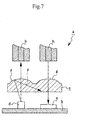
- the optical signal when the optical signal outputted from the light emitting element d is inputted to the lens body c , the optical signal may possibly inputted from the transmission side lens unit f to the light receiving element e as a stray light owing to reflection and double refraction generated in the lens body c , as shown with an arrow P in Fig. 7, which may result in deterioration of the optical signal inputted from the optical fiber h to the light receiving element e .
- the optical signal outputted from the light emitting element d toward the optical fiber h through the transmission side lens unit f may also reflects on a tip surface of the optical fiber h so that a stray light comes into the light receiving element e transmitting through the reception side lens unit g .
- an optical link device l having a light shielding plate k provided between a transmission side lens i and a reception side lens j which are separately formed (see Fig. 8).
- the optical signal outputted from the light emitting element d to be a stray light is shielded by the light shielding plate k and the stray light is prevented from coming into the light emitting element e .
- the optical link device l since a certain space for positioning the light shielding plate k is needed between the transmission side lens i and the reception side lens j , an interval between the lenses is required to be wide, which results in another problem that the optical link device becomes large.
- the optical link device of the present invention has an object to avoid deterioration of a signal due to a stray light coming into a light receiving element as well as to have a device smaller in size.
- an optical link device of the present invention is provided with a light emitting element to which an electrical signal is inputted and which converts the electrical signal into an optical signal so as to output it to one of optical fibers; a light receiving element to which an optical signal is inputted from the other of the optical fibers and which converts the optical signal into an electrical signal so as to output it; an element mounting unit on which the light emitting element and the light receiving element are mounted; and a lens body having a transmission side lens unit for guiding the optical signal outputted from the light emitting element to the one optical fiber and a reception side lens unit for guiding the optical signal outputted from the other optical fiber to the light receiving element, in which the transmission side lens unit and the reception side lens unit are integrally formed, and, in the device, a light shielding unit which is made of a material different from the transmission side lens unit and the reception side lens unit and formed integrally with the lens body between the transmission side lens unit and the reception side lens unit thereof is provided.
- another optical link device the present invention is provided with a light emitting element to which an electrical signal is inputted and which converts the electrical signal into an optical signal so as to output it to one of optical fibers; a light receiving element to which an optical signal is inputted from the other of the optical fibers and which converts the optical signal into an electrical signal so as to output it; an element mounting unit on which the light emitting element and the light receiving element are mounted; and a lens body having a transmission side lens unit for guiding the optical signal outputted from the light emitting element to the one optical fiber and a reception side lens unit for guiding the optical signal outputted from the other optical fiber to the light receiving element, in which the transmission side lens unit and the reception side lens unit are integrally formed, and, in the device, a light shielding cover having a pair of transmission holes through which the optical signal outputted from the light emitting element or the optical signal to be inputted to the light receiving element is transmitted, which is disposed between the lens body and the light emitting element and light receiving element.
- the lens body and the light emitting element and the light receiving element are separated by the light shielding cover.
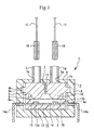
- An optical link device 1 comprises a box-shaped housing 2, and the housing 2 is made of a resin material (see Fig. 1).
- the housing 2 comprises a bottom plane portion 3, a side plane portion 4 which stands at an outer periphery of the bottom plane portion 3, and a top plane portion 5 positioned to face the bottom plane portion 3, and inside thereof is formed as a positioning space 2a.
- the housing 2 is divided by a plane including a center point of the bottom plane portion 3 and a center point of the top plane portion 5, for example.
- the side plane portion 4 has a plurality of insertion holes 4a, 4a, ... formed thereon.
- An installation groove 4b is formed on an inner surface of the side plane portion 4 at a position close to the top plane portion 5.
- the top plane portion 5 has installation holes 5a, 5a formed thereon separately having a space therebetween in a horizontal direction.
- each sleeves 6, 6 formed cylindrical with a ceramic material or a metal material is attached to fit each of the installation holes 5a, 5a of the top plane portion 5.
- a lens body 7 is arranged in the positioning space 2a of the housing 2.
- the lens body 7 comprises a sealing cap 8 formed cylindrical, a transmission side lens unit 9 provided inside of the sealing cap 8, a reception side lens unit 10 also provided inside the sealing cap 8 and a light shielding unit 11 provided between the transmission side lens unit 9 and the reception side lens unit 10, which are formed integrally.
- the sealing cap 8, the transmission side lens unit 9 and the reception side lens unit 10 are formed with a transparent resin material and the light shielding unit 11 is formed with a resin material different from the one forming the sealing cap 8, the transmission side lens unit 9 and the reception side lens unit 10.
- the light shielding unit 11 is formed with a material having a lower refractive index than the material for the sealing cap 8 or the like.
- the lens body 7 is formed by means of a so-called insert molding, in which a material of the sealing cap 8 and the like is filled in a mold in a condition that the light shielding unit 11 is positioned in the mold.
- Polyolefin materials including Zeonex (a product of Zeon Corporation) and Arton (product of JSR Corporation) are used for the transparent resin material for the sealing cap 8. Both the refractive indexes of Zeonex and Arton are 1.53.
- Quartz (refractive index 1.45) is used for a material of the light shielding unit 11, for example.
- a fluoric polymer material such as Opstar (a product of JSR Corporation) can be used as a material of the light shielding unit 11.
- the refractive index of Opstar is 1.36 to 1.42.
- the light shielding unit 11 of the lens body 7 has a function of reflecting a stray light and preventing the stray light from coming from the transmission side lens unit 9 into the reception side lens unit 10 when an optical signal outputted from a light emitting element to be described later becomes the stray light.
- the light shielding unit 11 only needs to have a function of reflecting at least a part of the optical signal inputted to the transmission side lens unit 9 and shielding it. However, it is desirable that the light shielding unit 11 has a function of total reflection, that is, reflecting all the stray lights.
- an incident angle of the stray light against the light shielding unit 11 is ⁇ ; a refractive index of the light shielding unit 11 is N1; and a refractive index of the sealing cap 8 and the like is N2
- a conditions for total reflection is defined as: sin ⁇ > N1/N2 and N2sin ⁇ > N1. Since the incident angle is in a range of 0° to 90° and it is defined as 0 ⁇ sin ⁇ ⁇ 1, it is desirable that N1 is as small as possible with regard to N2, taking a minimum value of sin ⁇ being 0 in consideration. Accordingly, it is desirable that the lens body 7 employs a material having a refractive index as small as possible compared to that of a material of the sealing cap 8, for the light shielding unit 11.
- an air gap may be formed between the transmission side lens unit 9 and the reception side lens unit 10 and may be used as a light shielding unit 11A.
- the light shielding unit 11 may be also possible to employ an opaque body for the light shielding unit 11. It is preferable that a material having a higher melting point than that of the resin material making up of the sealing cap 8 and the like is used for the opaque body. If the light shielding unit 11 employs the opaque body, it is possible to absolutely prevent the stray light from going into the reception side lens unit 10.
- a wavelength absorbing material which absorbs a wavelength that the optical signal outputted from the light emitting element has may be used as the light shielding unit 11.
- the wavelength of light used in the optical link device 1 is generally in a range of 650 nm to 780 nm, and it is desirable that a material absorbing a wavelength in this range for the wavelength absorbing material.
- the wavelength absorbing material a thin film formed with silicon dioxide and titanium dioxide (refractive index 1.45) may be used, for example. Even if the light shielding unit 11 is made of the wavelength absorbing material, it is also possible to absolutely prevent the stray light from going into the reception side lens unit 10. In this case, the whole light shielding unit 11 may be made of a material absorbing wavelengths and the light shielding unit 11 may be made by coating the material absorbing wavelengths on a surface of the metal material or the resin material.
- the opaque body or the wavelength absorbing material is employed for the light shielding unit 11, it is possible to prevent the stray light inputted to the reception side lens unit 10 irrespective of the incident angle of the stray light into the light shielding unit 11.
- the light shielding unit 11 may be formed with not only the resin material but also various materials including a metal material and a ceramic material, for example.
- the portion to be installed 8a is fitted in the installation groove 4b of the housing 2 to be attached to the housing 2.
- the optical communication package 12 comprises an element mounting unit 13 formed with a resin material, a lead frame 14 a part of which is attached on the element mounting unit 13, a light emitting element 15 and a light receiving element 16 which are provided as a photoelectric conversion element.
- the element mounting unit 13 comprises an element disposing portion 13a and a peripheral wall portion 13b standing from a fringe of the element disposing portion 13a.
- the lead frame 14 has external pins 14a, 14a ... projected outwardly from the element mounting unit 13.
- the external lead pins 14a, 14a ... are projected outwardly from the insertion holes 4a, 4a ... of the housing 2, respectively, to be connected to each connection unit of an external device such as a personal computer.
- the lens body 7 is fixed at the peripheral wall portion 13b of the element mounting unit 13 in a state that one end plane of the sealing cap 8 abuts on the peripheral wall portion 13b. Fixing the lens body 7 on the element mounting unit 13 seals the light emitting element 15 and the light receiving element 16 air-tightly. The light emitting element 15 and the light receiving element 16 air-tightly sealed with the lens body 7 prevents dew condensation due to environmental temperature changes and improves reliability in operation of the light emitting element 15 and the light receiving element 16.
- the light emitting element 15 and the light receiving element 16 are positioned to face the transmission side lens unit 9 and the receiving side lens unit 10 of the lens body 7, respectively.
- Optical fibers 17, 17 to be connected to the optical link device 1 are covered with ferrules 18, 18 at each tip portion.
- the optical fibers 17, 17 are inserted into the sleeves 6, 6 together with the ferrules 18, 18, and the tip planes thereof abut on the transmission side lens unit 9 and the reception side lens unit 10 of the lens body 7, respectively, to be positioned with regard to the optical link device 1 and to be jointed.
- the optical signal outputted from the light emitting element 15 is inputted into the transmission side lens unit 9 of the lens body 7, and is converged by the transmission side lens unit 9 to be inputted to the one optical fiber 17 so that data is transmitted and received.
- the optical signal outputted from the light emitting element 15 and inputted to the transmission side lens unit 9 sometimes reflects or is double-refracted in the lens body 7 to go toward the reception side lens unit 10 as a stray light.
- the light shielding unit 11 provided in the lens body 7 shields the stray light and the stray light is prevented from coming into the reception side lens unit 10.
- the transmitted optical signal is outputted from the optical fiber 17 toward the light receiving element 16.
- the optical signal outputted from the other optical fiber 17 is inputted to the reception side lens unit 10 of the lens body 7, and is inputted to the light receiving element 16 from the reception side lens unit 10.
- the optical signal inputted to the light receiving element 16 is photoelectrically converted in the light receiving element 16 so that an electrical signal is generated.
- the electrical signal is inputted to an external device through the external lead pin 14a so that the data is received.
- the optical link device 1 since the light shielding unit 11 is formed in the lens body 7 in which the sealing cap 8, the transmission side lens unit 9 and the reception side lens unit 10 are integrally formed, it is possible to prevent the optical signal which was outputted from the light emitting element 15 and inputted to the transmission side lens unit 9 from coming into the light receiving element 16 and to avoid deterioration of the signal inputted to the light receiving element 16.
- the light shielding unit 11 is formed integrally in the lens body 7, it is not necessary to dispose the transmission side lens unit 9 and the reception side lens unit 10 separately so that it becomes possible to reduce the number of parts constituting the optical link device 1 and the size thereof.
- optical link device 1 Furthermore, it is also possible to reduce the manufacturing cost of the optical link device 1 by integrally forming the light shielding unit 11 together with the transmission side lens unit 9 and the reception side lens 10 unit.
- an optical link device 1A of the second embodiment as described below is different from the optical link device 1 of the first embodiment as described above only in that it has no light shielding unit in the lens body and has a light shielding cover for covering a light emitting element. Accordingly, only portions different from the optical link device 1 will be described in detail and the other portions are numbered with same reference numerals as those in the optical link device 1 and precise description thereof will be omitted.
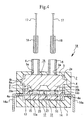
- a lens body 7A of the optical link device 1A comprises a sealing cap 8, a transmission side lens unit 9 and a reception side lens unit 10 integrally formed with a transparent resin material, and it has no light shielding unit 11 as provided in the lens body 7 of the optical link device 1 (see Fig. 4).
- the portion to be installed 8a is fitted in an installation groove 4b of a housing 2 so as to be attached to the housing 2.
- An optical communication package 12 has a light shielding cover 19 covering a light emitting element 15 and a light receiving element 16 attached thereto (see Fig. 4 and Fig. 5).
- the light shielding cover 19 is made of a metal material, such as die-casted aluminum, and is grounded to a not-shown ground circuit formed in an element mounting unit 13 of the optical communication package 12.
- the light shielding cover 19 comprises a covering portion 20 formed flatly and a partition portion 21 hanging down from a center portion in a horizontal direction of the covering portion 20.
- the covering portion 20 has transmission holes 20a and 20b respectively provided to oppose with each other having the partition portion 21 therebetween.
- an outer shape of the covering portion 20 is formed to have a size and a shape identical to those of an opening of the element mounting unit 13 of the optical communication package 12, and the covering portion 20 is adhered to a rim of the opening of the element mounting unit 13.
- the light emitting element 15 and the light receiving element 16 are partitioned with the partition portion 21, and the transmission holes 20a and 20b of the light shielding cover 19 are positioned in correspondence with the light emitting element 15 and the light receiving element 16, respectively.
- optical link device 1A In a condition that optical fibers 17, 17 are jointed to the optical link device 1A, when an electrical signal is inputted from an external device to the light emitting element 15 through an external lead pin 14a, an optical signal is generated through photoelectric conversion by the light emitting element 15 and the optical signal (laser beam) is outputted from the light emitting element 15 to one of the optical fibers 17.
- the optical signal outputted from the light emitting element 15 is transmitted through the transmission hole 20a of the light shielding cover 19 to be inputted into the transmission side lens unit 9 of the lens body 7A, and is converged by the transmission side lens unit 9 to be inputted to the one optical fiber 17 so that data is transmitted and received.
- the optical signal outputted from the light emitting element 15 and inputted to the transmission side lens unit 9 sometimes reflects or is double-refracted in the lens body 7 to be a stray light.
- the light receiving element 16 is covered with the light shielding cover 19 so that the stray light is prevented from coming into the light receiving element 16.
- the generated electromagnetic noise is prevented from propagating to the light receiving element 16.
- the transmitted optical signal is outputted from the optical fiber 17 toward the light receiving element 16.
- the optical signal outputted from the other optical fiber 17 is inputted to the reception side lens unit 10 of the lens body 7A, and is inputted from the reception side lens unit 10 to the light receiving element 16 through the transmission hole 20b.
- the optical signal inputted to the light receiving element 16 is photoelectrically converted to be an electrical signal.
- the electrical signal is inputted to an external device through the external lead pin 14a so that data reception is carried out.
- the light shielding cover 19 is disposed between the lens body 7 and the light emitting element 15 and light receiving element 16, it is possible to prevent the optical signal which was outputted from the light emitting element 15 and inputted to the transmission side lens unit 9 to be the stray light from coming into the light receiving element 16 and to avoid deterioration of the signal inputted to the light receiving element 16.
- the light emitting element 15 and the light receiving element 16 are partitioned with the partition portion 21, it is possible to reduce adverse effects on the light receiving element 16 due to the generated electromagnetic noise.
- the light shielding cover 19A of the modified example is made of a metal material and is grounded to a not-shown ground circuit formed in an element mounting unit 13 of an optical communication package 12.
- the light shielding cover 19A comprises a covering portion 22 formed flatly, a peripheral wall portion 23 hanging down from a peripheral edge of the covering portion 22 and a partition portion 24 hanging down from a center portion in a horizontal direction of the covering portion 22.
- the covering portion 22 has transmission holes 22a and 22b provided to oppose with each other having the partition portion 24 therebetween.
- an outer shape of the covering portion 22 is formed to have a size and a shape identical to those of an opening of the element mounting unit 13 of the optical communication package 12, and in a condition that the peripheral wall portion 23 is disposed to fit inside the element mounting unit 13, the covering portion 22 is adhered to a rim of the opening of the element mounting unit 13, for example.
- the light emitting element 15 and the light receiving element 16 are partitioned with the partition portion 24, and they are also surrounded by and covered with the peripheral wall portion 23.
- the transmission holes 22a and 22b of the light shielding cover 19 are positioned in correspondence with the light emitting element 15 and the light receiving element 16, respectively.
- the light shielding cover 19A instead of the light shielding cover 19, it is possible to avoid adverse effect on the external device such as a personal computer because the generated electromagnetic noise is hardly propagated outwardly owing to the arrangement in which the light emitting element 15 and the light receiving element 16 are surrounded by and covered with the peripheral wall portion 23, in addition to the effect similar to those obtained with the light shielding cover 19.
- the light shielding cover 19 and the light shielding cover 19A being formed with the metal material have been described in the above.
- the light shielding cover 19 and the light shielding cover 19A may be made of not only the metal material but also various materials including a resin material and a ceramic material. It is possible to prevent the stray light from coming into the reception side lens unit 10 in this case.
- Shapes and structures of respective portions described in each embodiment are only examples for substantiating the present invention in practical use, and therefore, the scope of the present invention should not be interpreted limitedly with these examples.
- the optical link device of the present invention is an optical link device to which a pair of optical fibers through which an optical signal is transmitted are connected to carry out data transmission and reception, which is characterized by comprising: a light emitting element to which an electrical signal is inputted and which converts the electrical signal into an optical signal so as to output it to one of the optical fibers; a light receiving element to which an optical signal is inputted from the other of the optical fibers and which converts the optical signal into an electrical signal so as to output it; an element mounting unit on which the light emitting element and the light receiving element are mounted; and a lens body having a transmission side lens unit for guiding the optical signal outputted from the light emitting element to the one optical fiber and a reception side lens unit for guiding the optical signal outputted from the other optical fiber to the light receiving element, in which the transmission side lens unit and the reception side lens unit are integrally formed, and the device is characterized in that a light shielding unit formed integrally with the lens body, which is made of a material different
- the optical signal outputted from the light emitting element and inputted to the transmission side lens is a stray light from coming into the reception side lens unit, and to avoid deterioration of the signal to be inputted to the light receiving element.
- the light shielding unit is formed integrally in the lens body, it is not necessary to dispose the transmission side lens unit and the reception side lens unit separately so that it becomes possible to reduce the number of parts constituting the optical link device and the size thereof.
- the optical link device it is also possible to reduce the manufacturing cost of the optical link device by integrally forming the light shielding unit together with the transmission side lens unit and the reception side lens unit.
- the material for forming the light shield is a material having a refractive index lower than that of a material for forming the transmission side lens unit and the reception side lens unit so that the material can be selected from a wide selection range and an amount of the optical signal changed to be the stray light coming into the reception side lens unit can be absolutely reduced.
- the opaque body is used for the light shielding unit so that the stray light is absolutely prevented from going into the reception side lens unit.
- the wavelength absorbing material which absorbs the wavelength that the optical signal outputted from the light emitting element has is used for the light shielding unit so that the stray light is absolutely prevented from coming through from the transmission side lens unit to the reception side lens unit.
- Another optical link device of the present invention is an optical link device to which a pair of optical fibers through which an optical signal is transmitted are connected to carry out data transmission and reception, which is characterized by comprising: a light emitting element to which an electrical signal is inputted and which converts the electrical signal into an optical signal so as to output it to one of optical fibers; a light receiving element to which an optical signal is inputted from the other optical fiber and which converts the optical signal into an electrical signal so as to output it; an element mounting unit on which the light emitting element and the light receiving element are mounted; and a lens body having a transmission side lens unit for guiding the optical signal outputted from the light emitting element to the one optical fiber and a reception side lens unit for guiding the optical signal outputted from the other optical fiber to the light receiving element, in which the transmission side lens unit and the reception side lens unit are integrally formed, and the device is characterized in that a light shielding cover having a pair of transmission holes through which the optical signal outputted from the light emitting element or the optical signal to be input
- the optical signal outputted from the light emitting element and inputted to the transmission side lens unit to be a stray light from coming into the light receiving element, and to avoid deterioration of the signal to be inputted to the light receiving element.
- the light shielding cover is formed with the metal material and the light shielding cover is grounded, even if the electromagnetic noise is generated when the optical signal is emitted from the light emitting element, the generated electromagnetic noise is hardly propagated to the light receiving noise, and it is possible to reduce adverse effects on the light receiving element due to the electromagnetic noise.
- the light shielding cover is provided with the partition portion between the light emitting element and the light receiving element, even if the electromagnetic noise is generated when the optical signal is emitted from the light emitting element, the generated electromagnetic noise is prevented from propagating to the light receiving noise, and it is possible to avoid adverse effects on the light receiving element due to the electromagnetic noise.
Landscapes
- Physics & Mathematics (AREA)
- General Physics & Mathematics (AREA)
- Optics & Photonics (AREA)
- Optical Couplings Of Light Guides (AREA)
- Mechanical Coupling Of Light Guides (AREA)
Abstract
Description
Claims (8)
- An optical link device to which a pair of optical fibers through which an optical signal is transmitted are connected to carry out data transmission and reception, characterized by comprising:characterized in that:a light emitting element to which an electrical signal is inputted and which converts the electrical signal into an optical signal so as to output to one of the optical fibers;a light receiving element to which an optical signal is inputted from the other of the optical fibers and which converts the optical signal into an electrical signal so as to output it;an element mounting unit on which the light emitting element and the light receiving element are mounted; anda lens body having a transmission side lens unit for guiding the optical signal outputted from the light emitting element to the one optical fiber and a reception side lens unit for guiding the optical signal outputted from the other optical fiber to the light receiving element, in which the transmission side lens unit and the reception side lens unit are integrally formed, anda light shielding unit formed integrally with the lens body, which is made of a material different from the transmission side lens unit and the reception side lens unit is provided between the transmission side lens unit and the reception side lens unit thereof.
- The optical link device as claimed in claim 1, characterized in that a material whose refractive index is lower than that of a material forming the transmission side lens unit and the reception side lens unit is used for forming said light shielding unit.
- The optical link device as claimed in claim 1, characterized in that an opaque body is used for said light shielding unit.
- The optical link device as claimed in claim 1, characterized in that a wavelength absorbing material for absorbing a wavelength that the optical signal outputted from the light emitting element has is used for said light shielding unit.
- An optical link device to which a pair of optical fibers through which an optical signal is transmitted are connected to carry out data transmission and reception, characterized by comprising:characterized in that:a light emitting element to which an electrical signal is inputted and which converts the electrical signal into an optical signal so as to output to one of the optical fibers;a light receiving element to which an optical signal is inputted from the other of the optical fibers and which converts the optical signal into an electrical signal so as to output it;an element mounting unit on which the light emitting element and the light receiving element are mounted, anda lens body having a transmission side lens unit for guiding the optical signal outputted from the light emitting element to the one optical fiber and a reception side lens unit for guiding the optical signal outputted from the other optical fiber to the light receiving element, in which the transmission side lens unit and the reception side lens unit are integrally formed, anda light shielding cover having a pair of transmission holes through which the optical signal outputted from the light emitting element or the optical signal to be inputted to the light receiving element is transmitted is disposed between the lens body and the light emitting element and light receiving element.
- The optical link device as claimed in claim 5, characterized in that said light shielding cover is formed with a metal material and the light shielding cover is grounded.
- The optical link device as claimed in claim 5, characterized in that a partition portion positioned between the light emitting element and the light receiving element is provided in said light shielding cover.
- The optical link device as claimed in claim 6, characterized in that a partition portion positioned between the light emitting element and the light receiving element is provided in said light shielding cover.
Applications Claiming Priority (3)
| Application Number | Priority Date | Filing Date | Title |
|---|---|---|---|
| JP2002138612 | 2002-05-14 | ||
| JP2002138612A JP2003329895A (en) | 2002-05-14 | 2002-05-14 | Optical link device |
| PCT/JP2003/005938 WO2003096096A1 (en) | 2002-05-14 | 2003-05-13 | Optical link device |
Publications (3)
| Publication Number | Publication Date |
|---|---|
| EP1505421A1 true EP1505421A1 (en) | 2005-02-09 |
| EP1505421A4 EP1505421A4 (en) | 2006-02-15 |
| EP1505421B1 EP1505421B1 (en) | 2007-09-19 |
Family
ID=29416871
Family Applications (1)
| Application Number | Title | Priority Date | Filing Date |
|---|---|---|---|
| EP03721099A Expired - Lifetime EP1505421B1 (en) | 2002-05-14 | 2003-05-13 | Optical link device |
Country Status (8)
| Country | Link |
|---|---|
| US (1) | US7121744B2 (en) |
| EP (1) | EP1505421B1 (en) |
| JP (1) | JP2003329895A (en) |
| KR (1) | KR20040111320A (en) |
| CN (1) | CN1281992C (en) |
| DE (1) | DE60316430T2 (en) |
| TW (1) | TWI226135B (en) |
| WO (1) | WO2003096096A1 (en) |
Cited By (1)
| Publication number | Priority date | Publication date | Assignee | Title |
|---|---|---|---|---|
| CN112444925A (en) * | 2019-08-27 | 2021-03-05 | 矢崎总业株式会社 | Optical connector |
Families Citing this family (30)
| Publication number | Priority date | Publication date | Assignee | Title |
|---|---|---|---|---|
| WO2004027880A2 (en) * | 2002-09-17 | 2004-04-01 | Koninklijke Philips Electronics N.V. | Camera device, method of manufacturing a camera device, wafer scale package |
| JP4053962B2 (en) * | 2003-10-15 | 2008-02-27 | 株式会社東芝 | Semiconductor device |
| JP4210240B2 (en) * | 2004-06-03 | 2009-01-14 | ローム株式会社 | Optical communication module |
| TWI404985B (en) | 2004-11-04 | 2013-08-11 | Hosiden Corp | Optical coupling components for optical communication connectors |
| JP4559952B2 (en) * | 2004-11-04 | 2010-10-13 | ホシデン株式会社 | Optical coupling member for optical communication connector, optical connector using the same, and optical connector assembling method |
| WO2006118285A1 (en) | 2005-04-27 | 2006-11-09 | Seiko Epson Corporation | Fluid transport system and fluid discharge amount setting method |
| DE102005059161A1 (en) * | 2005-12-12 | 2007-06-21 | Robert Bosch Gmbh | Optical module and method for mounting an optical module |
| JP4770551B2 (en) * | 2006-03-29 | 2011-09-14 | 富士ゼロックス株式会社 | Optical module |
| JP4943739B2 (en) * | 2006-05-18 | 2012-05-30 | 浜松ホトニクス株式会社 | Optical transceiver device |
| JP4740040B2 (en) * | 2006-05-31 | 2011-08-03 | 株式会社フジクラ | Optical communication module and manufacturing method thereof |
| JP4676975B2 (en) * | 2007-09-13 | 2011-04-27 | シャープ株式会社 | Bi-directional optical transmission device |
| JP2008286196A (en) * | 2008-05-13 | 2008-11-27 | Seiko Epson Corp | Communication device |
| GB2463226B (en) * | 2008-07-22 | 2011-01-12 | Conjunct Ltd | Optical sub-assembly |
| JP5222233B2 (en) | 2009-06-16 | 2013-06-26 | 株式会社オートネットワーク技術研究所 | Optical communication module |
| CN104793299B (en) * | 2009-09-18 | 2020-10-16 | 英特尔公司 | Combined optical and electrical interface |
| JP5505140B2 (en) * | 2010-07-05 | 2014-05-28 | 富士通株式会社 | Optical module and manufacturing method |
| KR101176950B1 (en) * | 2010-09-17 | 2012-08-30 | 주식회사 유나이브 | Optical transmitter, optical receiver for passive alignment of parts and method for passive alignment of parts |
| CN103620779B (en) | 2011-07-19 | 2016-12-28 | 赫普塔冈微光有限公司 | Photoelectric module and manufacturing method thereof |
| JP2015180914A (en) * | 2014-03-04 | 2015-10-15 | 株式会社東芝 | Optical link device |
| US20150270900A1 (en) * | 2014-03-19 | 2015-09-24 | Apple Inc. | Optical data transfer utilizing lens isolation |
| TWI667767B (en) | 2014-03-31 | 2019-08-01 | 菱生精密工業股份有限公司 | Package structure of integrated optical module |
| CN107402423A (en) * | 2016-05-18 | 2017-11-28 | 刘向宁 | A kind of photoconverter |
| CN108206397B (en) * | 2016-12-16 | 2021-12-24 | 富士康(昆山)电脑接插件有限公司 | Connector assembly |
| JP6666942B2 (en) * | 2018-03-20 | 2020-03-18 | 株式会社フジクラ | Optical module manufacturing method, optical module, and photoelectric conversion component |
| US10950743B2 (en) | 2019-05-02 | 2021-03-16 | Stmicroelectronics (Research & Development) Limited | Time of flight (TOF) sensor with transmit optic providing for reduced parallax effect |
| US11890466B2 (en) | 2019-07-01 | 2024-02-06 | Wavegate Corporation | IPG and header combination |
| JP2022050209A (en) * | 2020-09-17 | 2022-03-30 | 住友電気工業株式会社 | Optical module and optical connector cable |
| CN113467016A (en) * | 2021-06-29 | 2021-10-01 | 武汉光迅科技股份有限公司 | Light receiving assembly and optical module |
| CN116338872A (en) * | 2021-12-23 | 2023-06-27 | 深圳市速腾聚创科技有限公司 | A silicon optical chip packaging structure and packaging method |
| CN219695510U (en) * | 2023-03-06 | 2023-09-15 | Oppo广东移动通信有限公司 | Light detection component, lens and electronic equipment |
Family Cites Families (20)
| Publication number | Priority date | Publication date | Assignee | Title |
|---|---|---|---|---|
| JPS5849903A (en) | 1981-09-21 | 1983-03-24 | Canon Inc | Light shielding device for microlens |
| JPS5956779A (en) * | 1982-09-25 | 1984-04-02 | Toshiba Corp | Photosensor |
| US4572611A (en) * | 1983-08-04 | 1986-02-25 | Corning Glass Works | Apparatus including an integral optical device |
| JPS61226701A (en) * | 1985-03-29 | 1986-10-08 | Sharp Corp | Lens array |
| JP2718689B2 (en) * | 1988-03-09 | 1998-02-25 | 株式会社リコー | Lens array |
| US5093879A (en) * | 1990-06-22 | 1992-03-03 | International Business Machines Corporation | Electro-optical connectors |
| US5648874A (en) * | 1994-06-29 | 1997-07-15 | Fujitsu Limited | Optical apparatus |
| US5973844A (en) * | 1996-01-26 | 1999-10-26 | Proxemics | Lenslet array systems and methods |
| US5848211A (en) * | 1996-08-28 | 1998-12-08 | Hewlett-Packard Company | Photonics module having its components mounted on a single mounting member |
| JPH10126002A (en) * | 1996-10-23 | 1998-05-15 | Matsushita Electron Corp | Optical transmission module |
| US6289155B1 (en) * | 1997-12-13 | 2001-09-11 | Lightchip, Inc. | Wavelength division multiplexing/demultiplexing devices using dual high index of refraction crystalline lenses |
| JPH11187392A (en) * | 1997-12-19 | 1999-07-09 | Smk Corp | Two-way optical communication device |
| JP2000066064A (en) * | 1998-08-24 | 2000-03-03 | Hitachi Ltd | Optical transmission element, method of manufacturing the same, and optical transmission module |
| US6545811B1 (en) * | 1999-01-29 | 2003-04-08 | Rohm Co., Ltd. | Lens unit for image formation, and image reader having lens unit |
| TW594093B (en) * | 1999-10-19 | 2004-06-21 | Terashima Kentaro | Optical transmission and reception system, and optical transmission and reception module and optical cable for the system |
| JP2001174675A (en) * | 1999-12-21 | 2001-06-29 | Nec Corp | Optical waveguide type module |
| JP2001242348A (en) * | 1999-12-24 | 2001-09-07 | Asahi Kasei Corp | Optical communication method and optical communication link |
| US6707613B2 (en) * | 2000-04-05 | 2004-03-16 | Rohm Co., Ltd. | Lens array unit and method of forming image |
| JP2001343506A (en) * | 2000-06-01 | 2001-12-14 | Rohm Co Ltd | Method for producing lens array, lens array and method for subjecting lens array to shading treatment |
| US6635941B2 (en) * | 2001-03-21 | 2003-10-21 | Canon Kabushiki Kaisha | Structure of semiconductor device with improved reliability |
-
2002
- 2002-05-14 JP JP2002138612A patent/JP2003329895A/en active Pending
-
2003
- 2003-05-13 WO PCT/JP2003/005938 patent/WO2003096096A1/en not_active Ceased
- 2003-05-13 EP EP03721099A patent/EP1505421B1/en not_active Expired - Lifetime
- 2003-05-13 DE DE60316430T patent/DE60316430T2/en not_active Expired - Fee Related
- 2003-05-13 US US10/483,250 patent/US7121744B2/en not_active Expired - Fee Related
- 2003-05-13 CN CNB038007533A patent/CN1281992C/en not_active Expired - Fee Related
- 2003-05-13 KR KR10-2004-7000207A patent/KR20040111320A/en not_active Ceased
- 2003-05-14 TW TW092113096A patent/TWI226135B/en not_active IP Right Cessation
Cited By (2)
| Publication number | Priority date | Publication date | Assignee | Title |
|---|---|---|---|---|
| CN112444925A (en) * | 2019-08-27 | 2021-03-05 | 矢崎总业株式会社 | Optical connector |
| CN112444925B (en) * | 2019-08-27 | 2022-03-29 | 矢崎总业株式会社 | Optical connector |
Also Published As
| Publication number | Publication date |
|---|---|
| DE60316430D1 (en) | 2007-10-31 |
| US20040175080A1 (en) | 2004-09-09 |
| TW200406067A (en) | 2004-04-16 |
| EP1505421A4 (en) | 2006-02-15 |
| DE60316430T2 (en) | 2008-06-19 |
| KR20040111320A (en) | 2004-12-31 |
| WO2003096096A1 (en) | 2003-11-20 |
| CN1281992C (en) | 2006-10-25 |
| CN1537245A (en) | 2004-10-13 |
| JP2003329895A (en) | 2003-11-19 |
| TWI226135B (en) | 2005-01-01 |
| EP1505421B1 (en) | 2007-09-19 |
| US7121744B2 (en) | 2006-10-17 |
Similar Documents
| Publication | Publication Date | Title |
|---|---|---|
| US7121744B2 (en) | Optical link device | |
| US11681019B2 (en) | Optical module with stray light baffle | |
| JP4391564B2 (en) | Bi-directional optical transceiver module using single-core optical fiber cable | |
| CN101641580A (en) | Spectroscope | |
| KR102671974B1 (en) | Image sensor package | |
| CN113820824A (en) | Optical lens, imaging module and electronic device | |
| JP2012220352A (en) | Gas component detector | |
| US8449204B2 (en) | Optical module | |
| US20080187321A1 (en) | Optical transceiver module | |
| JP2013182954A (en) | Optical communication module | |
| US7682090B2 (en) | Integrated focusing and reflecting structure in an optical assembly | |
| JP7387801B2 (en) | Optical module and reflective encoder | |
| US10739537B2 (en) | Optical receptacle and optical module | |
| US6714363B2 (en) | Optical lens device assembly | |
| CN116868099A (en) | Lighting device | |
| KR102458341B1 (en) | Receiving lens module LiDAR | |
| US20260016645A1 (en) | Optical module and optical connector cable | |
| CN108063149B (en) | I/O modules and electronic devices | |
| JP2000357816A (en) | Optical coupling device | |
| KR100820004B1 (en) | Bidirectional Optical Signal Transceiver | |
| JP3260936B2 (en) | Optical package | |
| JP2009230048A (en) | Optical module | |
| JP2002344008A (en) | Optical element module | |
| JPH0656445B2 (en) | Hybrid optical multiplexer / demultiplexer | |
| JPH06308357A (en) | Waveguide type optical module |
Legal Events
| Date | Code | Title | Description |
|---|---|---|---|
| PUAI | Public reference made under article 153(3) epc to a published international application that has entered the european phase |
Free format text: ORIGINAL CODE: 0009012 |
|
| 17P | Request for examination filed |
Effective date: 20040114 |
|
| AK | Designated contracting states |
Kind code of ref document: A1 Designated state(s): AT BE BG CH CY CZ DE DK EE ES FI FR GB GR HU IE IT LI LU MC NL PT RO SE SI SK TR |
|
| RBV | Designated contracting states (corrected) |
Designated state(s): AT BE BG DE FR GB |
|
| A4 | Supplementary search report drawn up and despatched |
Effective date: 20051230 |
|
| 17Q | First examination report despatched |
Effective date: 20060504 |
|
| GRAP | Despatch of communication of intention to grant a patent |
Free format text: ORIGINAL CODE: EPIDOSNIGR1 |
|
| RBV | Designated contracting states (corrected) |
Designated state(s): DE FR GB |
|
| GRAS | Grant fee paid |
Free format text: ORIGINAL CODE: EPIDOSNIGR3 |
|
| GRAA | (expected) grant |
Free format text: ORIGINAL CODE: 0009210 |
|
| AK | Designated contracting states |
Kind code of ref document: B1 Designated state(s): DE FR GB |
|
| REG | Reference to a national code |
Ref country code: GB Ref legal event code: FG4D |
|
| REF | Corresponds to: |
Ref document number: 60316430 Country of ref document: DE Date of ref document: 20071031 Kind code of ref document: P |
|
| EN | Fr: translation not filed | ||
| PLBE | No opposition filed within time limit |
Free format text: ORIGINAL CODE: 0009261 |
|
| STAA | Information on the status of an ep patent application or granted ep patent |
Free format text: STATUS: NO OPPOSITION FILED WITHIN TIME LIMIT |
|
| PGFP | Annual fee paid to national office [announced via postgrant information from national office to epo] |
Ref country code: DE Payment date: 20080522 Year of fee payment: 6 |
|
| ET | Fr: translation filed | ||
| REG | Reference to a national code |
Ref country code: FR Ref legal event code: EERR Free format text: CORRECTION DE BOPI 08/21 - BREVETS EUROPEENS DONT LA TRADUCTION N A PAS ETE REMISE A L INPI. IL Y A LIEU DE SUPPRIMER : LA MENTION DE LA NON-REMISE. LA REMISE DE LA TRADUCTION EST PUBLIEE DANS LE PRESENT BOPI. |
|
| 26N | No opposition filed |
Effective date: 20080620 |
|
| PG25 | Lapsed in a contracting state [announced via postgrant information from national office to epo] |
Ref country code: FR Free format text: LAPSE BECAUSE OF FAILURE TO SUBMIT A TRANSLATION OF THE DESCRIPTION OR TO PAY THE FEE WITHIN THE PRESCRIBED TIME-LIMIT Effective date: 20080523 |
|
| PGFP | Annual fee paid to national office [announced via postgrant information from national office to epo] |
Ref country code: GB Payment date: 20080514 Year of fee payment: 6 |
|
| GBPC | Gb: european patent ceased through non-payment of renewal fee |
Effective date: 20090513 |
|
| REG | Reference to a national code |
Ref country code: FR Ref legal event code: ST Effective date: 20100129 |
|
| PG25 | Lapsed in a contracting state [announced via postgrant information from national office to epo] |
Ref country code: FR Free format text: LAPSE BECAUSE OF NON-PAYMENT OF DUE FEES Effective date: 20090602 |
|
| PGFP | Annual fee paid to national office [announced via postgrant information from national office to epo] |
Ref country code: FR Payment date: 20080514 Year of fee payment: 6 |
|
| PG25 | Lapsed in a contracting state [announced via postgrant information from national office to epo] |
Ref country code: GB Free format text: LAPSE BECAUSE OF NON-PAYMENT OF DUE FEES Effective date: 20090513 |
|
| PG25 | Lapsed in a contracting state [announced via postgrant information from national office to epo] |
Ref country code: DE Free format text: LAPSE BECAUSE OF NON-PAYMENT OF DUE FEES Effective date: 20091201 |