EP1504528B1 - Verfahren und vorrichtung zum kombinieren von signalen - Google Patents
Verfahren und vorrichtung zum kombinieren von signalen Download PDFInfo
- Publication number
- EP1504528B1 EP1504528B1 EP03712447A EP03712447A EP1504528B1 EP 1504528 B1 EP1504528 B1 EP 1504528B1 EP 03712447 A EP03712447 A EP 03712447A EP 03712447 A EP03712447 A EP 03712447A EP 1504528 B1 EP1504528 B1 EP 1504528B1
- Authority
- EP
- European Patent Office
- Prior art keywords
- signal
- frequency
- input
- signals
- output
- Prior art date
- Legal status (The legal status is an assumption and is not a legal conclusion. Google has not performed a legal analysis and makes no representation as to the accuracy of the status listed.)
- Expired - Lifetime
Links
- 238000000034 method Methods 0.000 title claims abstract description 38
- 230000005540 biological transmission Effects 0.000 claims abstract description 94
- 230000001808 coupling effect Effects 0.000 claims abstract description 23
- 238000012360 testing method Methods 0.000 claims description 11
- 230000010363 phase shift Effects 0.000 claims description 10
- 230000000694 effects Effects 0.000 claims description 8
- 238000010998 test method Methods 0.000 claims description 5
- 238000002955 isolation Methods 0.000 description 6
- 239000003990 capacitor Substances 0.000 description 5
- 239000000758 substrate Substances 0.000 description 5
- 230000008878 coupling Effects 0.000 description 4
- 238000010168 coupling process Methods 0.000 description 4
- 238000005859 coupling reaction Methods 0.000 description 4
- 230000003321 amplification Effects 0.000 description 3
- 238000001914 filtration Methods 0.000 description 3
- 230000002452 interceptive effect Effects 0.000 description 3
- 238000003199 nucleic acid amplification method Methods 0.000 description 3
- 230000008901 benefit Effects 0.000 description 2
- 230000000903 blocking effect Effects 0.000 description 2
- 238000004458 analytical method Methods 0.000 description 1
- 238000012512 characterization method Methods 0.000 description 1
- 238000013461 design Methods 0.000 description 1
- 238000011161 development Methods 0.000 description 1
- 239000003989 dielectric material Substances 0.000 description 1
- 238000010438 heat treatment Methods 0.000 description 1
- 238000012545 processing Methods 0.000 description 1
- 238000012546 transfer Methods 0.000 description 1
- 238000010396 two-hybrid screening Methods 0.000 description 1
Images


Classifications
-
- H—ELECTRICITY
- H01—ELECTRIC ELEMENTS
- H01P—WAVEGUIDES; RESONATORS, LINES, OR OTHER DEVICES OF THE WAVEGUIDE TYPE
- H01P5/00—Coupling devices of the waveguide type
- H01P5/12—Coupling devices having more than two ports
- H01P5/16—Conjugate devices, i.e. devices having at least one port decoupled from one other port
Definitions
- This invention relates to a method of combining signals, a device for combining signals, a method of testing the performance of an electronic device and a testing kit for testing the performance of an electronic device.
- the invention relates, in particular, to bias T devices suitable for broadband, high power, and high current applications.
- a bias T is a type of signal combining device which can combine a first input signal with a second input signal to provide an output signal comprising a combination of the first and second inputs.
- the first and second inputs are independent from one another and are not affected in any substantial way by connection to the bias T device or its mode of operation.
- This type of device may also be referred to as a Bias "Tee" device.
- bias T devices are useful in device characterization and testing applications.
- bias T devices may be used to apply direct current (DC) offsets or level shifts in radio frequency (RF), pulsed radio frequency and base band testing of active devices.
- DC direct current
- RF radio frequency
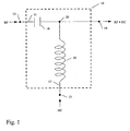
- FIG. 1 shows a known bias T device.
- the bias T device 10 comprises a first input terminal 12 for receiving a radio frequency (RF) varying signal, a second input terminal 13 for receiving a direct current (DC) signal and an output terminal 14 which comprises a combination of the radio frequency and DC signals.
- RF radio frequency
- DC direct current
- an output terminal 14 which comprises a combination of the radio frequency and DC signals.
- a radio frequency transmission line 15 is connected to the radio frequency input 12 and is provided with a capacitor 16.
- a direct current transmission line 17 connected to the direct current input 13 is provided with an inductor 18.
- the radio frequency and direct current transmission lines 15, 17 are connected at a node 20 located on the output side of respective components 16 and 18.
- the node 20 is connected to the output terminal 14.
- the capacitor 16 on the radio frequency transmission line 15 presents a low impedance to radio frequency signals and a high impedance to direct current.
- the capacitor 16 thus acts as a series blocking capacitor preventing the direct current signal from interfering with the radio frequency signal supplied to input 12.
- the inductor 18 on the direct current transmission line 17 presents a high impedance to radio frequency signals and a low impedance to direct current. Hence the inductor prevents the radio frequency signals which pass through the capacitor 16 from interfering with the direct current input signal supplied to input terminal 13.
- the known bias T device of Figure 1 would typically operate in direct current ranges of up to about half an amp and radio frequency ranges of up to 40GHz.
- the current handling and radio frequency handling of known bias T devices is limited because such devices typically modify signal flow by virtue of transmission line geometries, for example spiral wire structures or through the effects of components connected in series with the transmission lines.
- a problem with such devices is that high currents and/or.high radio frequency power cause heating effects which limit the range of applications of the devices. For instance, for broadband applications the inductor would need to be made from relatively thin conducting wire, thereby limiting the maximum current flow through the device.
- the invention seeks to provide an improved signal combining device.
- a bias T device for combining a first signal with a second signal
- the device comprising first and second couplers, wherein the first coupler has a first transmission line directly connected to a first transmission line of the second coupler and has a second transmission line directly connected to a second transmission line of the second coupler such that the signals passing from one coupler to the other coupler along the transmission lines are substantially unaffected, the first coupler is configured to receive a first input signal at a first input connected to the first transmission line and a second input signal at a second input connected to the second transmission line, the couplers are each configured to provide a coupling effect between the first and second transmission lines of the coupler, the coupling effect affecting only those signals having a frequency within a frequency range, and the device is configured to provide an output signal at an output connected to the first transmission line of the second coupler, whereby, in use, the device is able to produce at the output a combination of a first low frequency signal, for example a DC signal, outside the
- the couplers are advantageously 3dB 90° hybrid couplers, for example of the kind that are presently widely commercially available.
- the device is arranged such that signals outside the frequency range travelling along one of the first and second transmission lines of a coupler do so substantially without causing a corresponding signal to travel along the other transmission line of the coupler.
- the low frequency signals pass along the first transmission lines of the first and second couplers without experiencing the coupling effect, whereas high frequency signals within the frequency range experience coupling effects in the first and the second couplers resulting in an output signal being presented on the first transmission line of the second coupler in response to signals inputted at the second transmission line of the first coupler.
- the function that the device performs on input signals may therefore be considered as including a signal filtering function as well as a signal combining function.
- signal filters may be provided between the couplers, there is no need for such additional signal filters in this embodiment.
- the RF signal may include or consist of a rig having a fundamental frequency of greater than 500 MHZ
- the method may include the step of including a step of splitting the high frequency RF signal into first and second signal components and imparting a relative phase shift such that said first and second signal components have a predetermined phase offset.
- the method may include a further step of splitting each of said first and second signal components into at least two further signal components and imparting a further relative phase shift, such that said further signal components have a predetermined phase offset with respect to one another.
- the high frequency RF signal may be substantially reproduced by constructive interference effects between said further signal components.
- Each transmission line of the two couplers allows signals lower than the frequency band to pass substantially without attenuation.
- At least two of said transmission lines of one of the signal splitting circuits may be electrically connected to each other.
- the electrical connections between the respective two transmission lines of the first signal splitting circuit and the two transmission lines of the second signal splitting circuit may each include a high pass filter.
- the device may be so arranged that one of the first and second signal splitting circuits is adapted to receive the first input signal and the other one of the first and second signal splitting circuits is adapted to receive the second input signal.
- Respective signal paths of the device may include, or consist of, a wave guide and/or may comprise a microstrip transmission line.
- At least one, and more preferably each, of said first and second signal splitting circuits comprises a hybrid coupler.
- the hybrid coupler may be in the form of a 90° hybrid coupler, for example a quadrature hybrid coupler.
- the present invention also provides a method of combining signals having different fundamental frequencies, the method comprising the steps of:
- the method is of particular application where the first input signal has a fundamental frequency lower than the frequency band, and especially where the first input signal has a DC component.
- the first input signal may for example be a DC signal, with little or no higher order components.
- the second input signal may for example be a high frequency signal or an RF signal.
- the method advantageously includes a step of splitting the second input signal into first and second signal components.
- both of the first and second input signals may be split by the signal splitting circuits.
- the step of splitting the second input signal into first and second signal components advantageously includes imparting a relative phase shift such that said first and second signal components have a predetermined phase offset, which is preferably substantially 90 degrees.
- the method preferably includes a further step of splitting each of said first and second signal components into at least two further signal components and imparting a further relative phase shift, such that said further signal components have a predetermined phase offset with respect to one another, which again is preferably substantially 90 degrees.
- Said second input signal is advantageously substantially reproduced by constructive interference effects between said further signal components.
- the reproduction of the second input signal is preferably in the form of a signal comprising a combination of the first input signal and the reproduction (possibly phase shifted) of the second input signal, the resulting signal being receivable as an output signal.
- the method is advantageously able to produce an output signal comprising a summation of the input signals substantially without loss.
- Each transmission line of the two signal splitting circuits preferably allows signals lower than the frequency band to pass substantially without attenuation.
- high pass filtering may be applied to at least one of the signals between said first and second signal splitting circuits, said second input signal being substantially unaffected by the high pass filtering.
- the method of the present invention may conveniently be performed using first and second signal splitting circuits arranged in accordance with the bias T device according to the present invention.
- the present invention also provides a method of testing the performance of an electronic device, the method including a step of applying a high power electronic signal comprising a low frequency component and a high frequency component by means of the use of a bias T device according to the present invention or by means of a method of combining signals according to the present invention.
- the method of testing may be performed such that the low frequency component includes or consists of a DC signal and/or such that the high frequency component includes or consists of a signal having a fundamental frequency of greater than 500 MHz.
- a signal having a power greater than 10 Watts may be considered as being high power.
- the device and method of the present invention may be able to handle signals at powers significantly greater than 10 Watts, for example, at powers greater than 50 Watts.
- signals having a fundamental frequency greater than 500 MHz may be considered as being high frequency signals and signals substantially lower than 500MHz may be considered as being low frequency signals.
- the present invention yet further provides a testing kit including a bias T device according to the present invention, a low frequency power source and a high frequency power source.
- the testing kit is advantageously suitable for performing the method of testing the performance of an electronic device according to the present invention.
- the low frequency power source may be connected to a first input of a bias T device of the present invention to provide the low frequency component and the high frequency power source may be connected to a second input of the bias T device to provide the high frequency component, the output of the bias T device providing the high power electronic signal for testing the performance of a given electronic device.
- the testing method and kit of the present invention may be of particular application in relation to the analysis, development, design and improvement of high frequency, high power devices, for example, transistor devices or other components used in amplification and/or signal processing circuits used in high power broad band applications.
- Such applications may for example include amplification circuits used in mobile telecommunication base stations.
- the present invention is of particular application when the first signal is a DC signal and the second signal is an RF signal. It will however be appreciated that the present invention may also be of benefit in applications where first and second signals are combined, wherein the first signal is outside an operational frequency band and the second signal is within the operational frequency band.
- a device for combining a first signal outside a frequency range with a second signal within the frequency range comprising first and second signal splitting circuits, each having at least two transmission lines, the signal splitting circuits together being adapted to receive a first input signal at one input and a second input signal at another input, and to provide an output signal comprising a combination of said first input signal and said second input signal, wherein two transmission lines of the first signal splitting circuit are respectively electrically connected to two transmission lines of the second signal splitting circuit, and a coupling effect between at least two of the transmission lines effects, in use, the splitting of signals within the frequency range and the combination of said first input signal and said second input signal.
- a corresponding method may also be provided, such a method comprising the steps of providing two signal splitting circuits electrically connected to each other, the circuits together having two inputs and at least one output, each signal splitting circuit comprising at least two transmission lines, the signal splitting circuits splitting input signals within a frequency range between two transmission lines by virtue of a coupling effect between the lines, applying a first input signal having a fundamental frequency outside the frequency range to one of the two inputs, applying a second input signal having a fundamental frequency within the frequency range to the other of the two inputs, and outputting an output signal from said at least one output, the output signal comprising a combination of the first and second input signals, the combination being effected by the coupling effect of each of the two signal splitting circuits.
- the first input signal may be at a frequency higher than the second input signal.
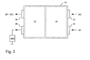
- FIG. 2 shows a high current bias T device 20 implemented using two back-to-back hybrid circuits.
- the bias T has a first input port 22 adapted to receive a direct current signal and a second input port 24 adapted to receive a radio frequency signal.
- the bias T device 20 has two further ports, the first of which 26 provides an output signal combining the signals at the input ports 22 and 24 and the second of which 28 is terminated by a 50 ⁇ load. This 50 ⁇ load is optional and is connected to the bias T in order to counter some imperfections of the hybrids as will be explained hereinafter.
- the bias T device 20 comprises a first 90° hybrid circuit 30 coupled to a second 90° hybrid circuit 32.
- the input ports 22 and 24 are provided on the first 90° hybrid circuit 30 and the output ports 26 and 28 are provided on the second 90° hybrid circuit 32.
- the bias T device of Figure 2 is used here to combine a radio frequency signal supplied at port 24 with a direct current signal supplied at port 22 to provide an output signal at port 26 comprising direct current and radio frequency components without either of the signals at ports 22 and 24 being perturbed in any way.
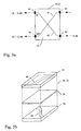
- Figure 3a and 3b illustrate a 90° hybrid circuit of the type used to implement the bias T device of Figure 2 .
- the schematic plan view of Figure 3a shows a transmission line 34 connecting a first input port 36 to a diagonally opposed output port 38.
- a second transmission line 40 connects a second input port 42 to a second diagonally opposed output port 44.
- the transmission lines 34,40 may be of any convenient type, for example they may be wave guides or microstrip lines. In this embodiment, the transmission lines are disposed within a block of dielectric material 50.
- the dielectric block 50 is comprised of an upper substrate 52, a thin isolation layer 54 and a lower substrate 56.
- a first metalised region 60 disposed on a lower surface of the upper substrate layer 52 defines the transmission line 34.
- a second metalised region 62 disposed on an upper surface of the lower substrate layer 56 defines the transmission line 40.
- the transmission lines 34,40 follow diagonal paths on opposed faces of the respective substrate layers 52,56.
- the isolation layer 54 disposed between the transmission lines 34,40 electrically isolates the transmission lines from each other.
- the inputs 36 and 42 are also electrically isolated from one another.
- the two transmission lines of each hybrid circuit are arranged in such a way that a coupling occurs between the lines for signals within the operational bandwidth of the 90° hybrid. For signals having frequencies outside the operational bandwidth of the hybrid circuits no coupling occurs (e.g. a DC signal) and isolation between the transmission lines is effective to prevent signals on different lines from mixing.
- Each 90° hybrid circuit 30,32 acts as a three decibel coupler with a transmission line 34 connected between ports 36 and 38 and a second transmission line 40 between ports 42 and 44.
- a direct current provided at the input port 36 will be supplied directly to the output port 38 without any current leaking onto the transmission line 40.
- the hybrid circuit would split a radio frequency signal having a frequency within the operational bandwidth into two separate radio frequency output signals.
- An input signal of X decibels would be split into two equal amplitude output signals at ports 44 and 38 and each having a power of X-3 decibels.
- a signal diagonally traversing a 90° hybrid circuit experiences a 90° phase shift relative to a signal following a straight through signal path.
- the radio frequency output signals at ports 44 and 38 are of equal amplitude and have a relative phase offset of 90°.
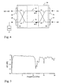
- Figure 4 shows the bias T device 20 of Figure 2 with signal routes through the device illustrated schematically.
- the two 90° hybrid circuits are coupled together such that the transmission line 34 of the first hybrid circuit 30 connects to the transmission line 40' of the second hybrid circuit 32. This forms a continuous signal path 72 between ports 22 and 26 of the device.
- the transmission line 40 of the first hybrid circuit 30 connects to transmission line 34' of the second hybrid circuit 32 forming a continuous signal path 70 between ports 24 and 28 of the device.
- the continuous paths are electrically isolated from one another by the isolation layers 54 in respective hybrid circuits 30,32. Signals within the operational bandwidth of the 90° hybrids experience a coupling effect and are transferred between the two transmission paths. Signals outside this operational bandwidth (e.g. a DC signal) do not couple and so cannot overcome the isolation between the transmission paths to transfer from one to the other.
- a DC signal e.g. a DC signal
- the direct current input at the port 22 of the first hybrid circuit 30 travels along the signal path 72 through the first hybrid circuit 30 and into the second hybrid circuit 32.
- the DC current signal is output at port 26 without any DC signal components affecting the signal on the signal path 70 or at either of the ports 24 and 28.
- a radio frequency signal which is input at port 24 does not follow a single path.
- the radio frequency signal is split into two separate signals as it passes through the first hybrid circuit 30.
- the splitting of the radio frequency is caused by a coupling between the transmission line 40 connected to port 24 and the transmission line 34 which is also used for the DC signal.
- the first RF 1 and second RF 2 radio frequency signals resulting from the coupling effect have a phase difference of 90°.
- the signals RF 1 and RF 2 are output from the first hybrid circuit 30 and supplied to the respective input ports of the second hybrid circuit 32.
- a coupling effect between transmission lines 34' and 40' of the second hybrid circuit 32 means that the radio frequency signal RF 1 received at the input connected to line 34' is partially coupled onto the transmission line 40'.
- the radio frequency signal RF 2 received at the input connected to line 40' is partially coupled onto transmission line 34'.
- Each of the signals RF 1 and RF 2 is split into two further signal components as they traverse the second hybrid circuit 32. Between these signal components an additional phase shift is imparted. As a result, the signal components interfere constructively at the output port 26. The signals interfere destructively at the output port 28 such that they can cancel each other out.
- phase offset within a hybrid is not exactly 90°C the signals at port 28 will not be exactly combined out-of-phase and hence they will not cancel each other out completely.
- the 50 ⁇ load absorbs the remaining signal preventing them from interfering with signals at port 26.
- the radio frequency signal input at the port 24 appears without loss at the output port 26 where it is combined with the direct current signal supplied to the other input port 22.
- the line losses and losses caused by imperfections are neglected within this specific description since they are small within the realized device. However, within other embodiments (e.g. using hybrids with larger imperfections) they may not be neglected.
- the above described embodiment thus uses a coupling effect between separate transmission lines in 90° hybrid circuits to combine a radio frequency signal with a DC signal.
- the coupling effect depends mainly on the distance between the two transmission lines and does not depend substantially on the width of the transmission lines. Accordingly, the above embodiment overcomes problems with the prior art in that thick transmission lines can be used in preferred embodiments. Therefore preferred embodiments need not be limited to low current ranges, low power high frequency signals, or narrow radio frequency operating bandwidths. Therefore, no trade-off is necessary between high DC current handling capability and broad bandwidth of the signal-combining device.
- Figure 5 shows transmission S-parameter results obtained using a bias T device according to Figure 2 .
- the hybrid circuits used were rated to pass signals at frequencies in the range of 1.3 to 10GHz.
- S-parameter results were obtained by connecting a suitable frequency generator to the input port 24 and measuring the response at the output port 26 of the bias T device 20.
- the bias T operates reliably in the bandwidth range 1.3 to 10GHz. Satisfactory results have been obtained using DC input currents of 10 or more amps.
- the embodiment described with reference to Figures 2 to 4 uses a DC signal at port 22.
- the device is suitable to combine any signals of which one is outside and the other within the operational bandwidth of the hybrids. That is, the above-described device would combine any signals input at port 22, which may be outside the operational bandwidth of the hybrid circuitry, with any signals input at port 24, which are within the operational bandwidth of the hybrid circuitry.
- the device in Figures 2 and 4 splits only the signal inserted at port 24 into multiple frequency components with a phase offset. As a result, the device may not require filters or other selective signal blocking means between the two hybrids. That is, the principle of operation relies on only one input signal component being split into multiple signals while the second signal is directly forwarded from one port to another without being split.
- Preferred embodiments such as the one illustrated in Figure 2 can therefore be used to combine two radio frequency signals. For example, this can be achieved by inputting a first radio frequency signal (having a frequency outside the operational bandwidth of the hybrid circuits) to input port 22 and inputting a second radio frequency signal (having a frequency within the operational bandwidth of the hybrid circuits) to input port 24.
- the signal output at port 26 is then a combination of the first and second RF signals input at ports 22 and 24.
- bias T devices with different operating ranges.
- other hybrid circuits have operating frequencies in the range 1 to 18GHz or more and so can extend the operating bandwidth of preferred bias T devices up to 18GHz.
- Other hybrid circuits can extend the operating bandwidth still further.
- Appropriately designed transmission lines will permit still higher operating currents.
- Preferred embodiments thus provide bias T devices which are operable at high currents, high frequencies with high power levels, and over large bandwidth ranges. Such bias T devices are useful for example in the testing of high powered transistors.
- preferred embodiments can also be used in many other applications, such as in amplification applications.
- FIG. 6 shows another bias T device embodying the present invention.
- the transmission lines (and inputs) of the hybrid circuits employed in this embodiment are not electrically isolated from one another.
- the bias T device comprises a first input port 122 for receiving a direct current signal and a second input port 124 for receiving a radio frequency signal.
- the bias T device 100 has two further ports, the first of which 126 provides an output signal which is a combination of the radio frequency and direct current signals at input ports 124 and 122.
- the second further port is an output port 128 terminated by an optional 50 electrical load.
- the bias T device 100 comprises a first 90° hybrid circuit 130 and a second 90° hybrid circuit 132.
- the radio frequency input port 124 is provided on the first hybrid circuit 130 and the direct current input port 122 is provided on the second hybrid circuit 132.
- High pass filters 180 and 182 are disposed between the first and second hybrid circuits 130,132, one on each of the signal paths as will be explained herein.
- the bias T device 100 of Figure 6 can combine a radio frequency signal supplied to the port 124 with a direct current signal supplied to the port 122 in order to provide an output signal comprising both radio frequency and direct current components without affecting either of the input signals in any way.
- FIGs 7a and 7b illustrate a hybrid circuit of the type described to implement the bias T device 100 of Figure 6 .
- the transmission lines are arranged to form a quadrilateral shape 134 with spurs 140 connecting to each of the input and output ports.
- the transmission lines 134,140 are formed by a metalised region disposed between dielectric layers 152,156. Since there is no isolation between any of the respective transmission lines (or the input and output terminals) the metalised region 160 of the 90° hybrid circuit may be regarded as a continuous transmission line system.
- Hybrid circuits of the type shown in Figure 7a and 7b can split a radio frequency signal input at port 136 into two radio frequency signals of substantially the same amplitude which are output at ports 144 and 138.
- the radio frequency signals output at ports 144 and 138 have a relative phase difference of 90° which is imparted to them by the hybrid circuit.
- Figure 8 shows the bias T device 100 of Figure 6 with signal paths through the device illustrated schematically.
- the two 90° hybrid circuits 130,132 are arranged as in a branch line coupler with two high pass filters 180,182 coupling them together.
- the high pass filters 180,182 are tuned so as to prevent the direct current passing while allowing the radio frequency signal to pass.
- the direct current signal input at port 122 of the second hybrid circuit 132 is blocked by the high pass filters 180,182.
- the direct current signal is output at port 126 of the second hybrid circuit 132 without passing into the first hybrid circuit 130.
- the radio frequency signal input at port 124 of the first hybrid circuit 130 is split into two separate signals RF 1 and RF 2 as it traverses the first hybrid circuit 130.
- the second radio frequency signals RF 1 and RF 2 output from the first hybrid circuit 130 have a relative phase offset of 90°.
- the radio frequency signals RF 1 and RF 2 pass through the respective high pass filters 180,182 and are input to the respective input ports of the second hybrid circuit 132.
- the radio frequency signals RF 1 and RF 2 are split into further radio frequency components while they traverse the second hybrid circuit 132.
- the output signals derived from radio frequency signal RF 1 have a 90° relative phase offset after they have traversed the hybrid circuit 132.
- the output signals derived from radio frequency signal RF 2 have a similar 90° phase offset after they have passed through the hybrid circuit 132. Accordingly, the signals derived from the signals RF 1 and RF 2 interfere constructively at the output port 126 and destructively at the output port 128. The result is that the radio frequency signal input at port 124 appears substantially without loss at the port 126 where it combines with the direct current signal also supplied to that port from port 122.
- a device is used to combine a radio frequency signal input at port 124 with a direct current signal input at port 122.
- the signal input at port 122 need not be a direct current signal.
- the signal input at port 122 may be an alternating signal having a frequency anywhere in the range between zero and the cut-off frequency of the high pass filters 180,182.
- the high pass filter can be selected to have a lower cut-off frequency between the frequencies of the signal input at port 124 and the signal input at port 122.
- the device of Figures 6 to 8 can be used to combine a first alternating signal input at point 124 with a second signal having a frequency anywhere between zero up to the cut-off frequency. It will be apparent that the signal input at port 122 can be inside or outside the operational bandwidth of the hybrid 132.
- Both embodiments described herein use hybrid circuits to recombine components of at least one of the input signals.
- a combining device receives first and second input signals.
- the first input signal is a direct current signal and the second input signal is a radio frequency signal.
- a first signal splitting means is supplied with the second input signal which it splits into first and second signal components.
- the first signal splitting means also imparts a relative phase shift to signals which pass through it such that the first and second signal components have a predetermined phase offset.
- a second signal splitting means is arranged to split each of the first and second signal components into at least two further signal components.
- the second signal splitting means also imparts a further relative phase shift to signals which pass through it such that the further signal components have a further predetermined phase offset.
- a representation of the second input signal is provided at an output where interference effects between the further signal components arise.
- the device outputs a combination of the first input signal and the representation of the second input. Owing to the nature of the interference effects which lead to the representation of the second input signal the signals are combined at the output substantially without any losses.
- Implementations of the invention should not be limited to the configurations of the described embodiments. Specifically, the described embodiments are examples of configurations which may be used to implement preferred methods and are not intended to define the only apparatus features/method steps which can be used.
Landscapes
- Transmitters (AREA)
- Amplitude Modulation (AREA)
- Amplifiers (AREA)
- Crystals, And After-Treatments Of Crystals (AREA)
- Diaphragms For Electromechanical Transducers (AREA)
- Investigating Or Analyzing Materials By The Use Of Ultrasonic Waves (AREA)
- Waveguide Connection Structure (AREA)
- Variable-Direction Aerials And Aerial Arrays (AREA)
Claims (16)
- Verfahren zum Kombinieren eines Gleichspannungssignals und eines Hochfrequenz-HF-Signals, wobei das Verfahren die Schritte aufweist:Bereitstellen zweier Koppler (30, 32), die jeweils mindestens zwei Übertragungsleitungen (34, 40) aufweisen, wobei die Koppler (34, 40) miteinander direkt elektrisch verbunden sind, so daß die Signale, die von einem Koppler zum anderen Koppler längs der Übertragungsleitungen gehen, im wesentlichen unbeeinflußt sind, wobei die Koppler zusammen zwei Eingänge (22, 24) und mindestens einen Ausgang (26) aufweisen, wobei die Koppler Eingangssignale innerhalb eines Frequenzbands zwischen zwei Übertragungsleitungen vermöge eines Kopplungseffekts zwischen den Leitungen aufteilen,Anlegen eines Gleichspannungssignals außerhalb des Frequenzbands an einen der beiden Eingänge (22),Anlegen eines Hochfrequenz-HF-Signals mit einer Grundfrequenz innerhalb des Frequenzbands an den anderen der beiden Eingänge (24),Ausgeben eines Ausgangssignals aus dem mindestens einen Ausgang (26), wobei das Ausgangssignal eine Kombination des Gleiehspannungssignals und des Hochfrequenz-HF-Signals aufweist, wobei die Kombination durch den Kopplungseffekt von jedem der beiden Koppler bewirkt wird.
- Verfahren nach Anspruch 1, wobei das HF-Signal ein Signal mit einer Grundfrequenz von mehr als 500 MHz aufweist oder aus ihm besteht.
- Verfahren nach einem der Ansprüche 1 oder 2, wobei das Verfahren einen Schritt des Aufteilens des Hochfrequenz-HF-Signals in erste und zweite Signalkomponenten und des Verleihens einer relativen Phasenverschiebung aufweist, so daß die ersten und zweiten Signalkomponenten einen vorgegebenen Phasenversatz aufweisen.
- Verfahren nach Anspruch 3, wobei das Verfahren einen weiteren Schritt des Aufspaltens jeder der ersten und zweiten Signalkomponenten in mindestens zwei weitere Signalkomponenten und des Verleihens einer weiteren relativen Phasenverschiebung aufweist, so daß die weiteren Signalkomponenten in Bezug zueinander einen vorgegebenen Phasenversatz aufweisen.
- Verfahren nach Anspruch 4, wobei das Hochfrequenz-HF-Signal im wesentlichen durch konstruktive Interferenzeffekte zwischen den weiteren Signalkomponenten reproduziert wird.
- Verfahren nach einem der Ansprüche 1 bis 5, wobei jede Übertragungsleitung der beiden Koppler Signale, die niedriger als das Frequenzband sind, im wesentlichen ohne Abschwächung passieren läßt.
- Bias-T-Vorrichtung zum Kombinieren eines ersten Signals mit einem zweiten Signal, wobei die Vorrichtung erste und zweite Koppler (30, 32) aufweist, wobei der erste Koppler (30) eine erste Übertragungsleitung (34) aufweist, die direkt mit einer ersten Übertragungsleitung (40) des zweiten Kopplers verbunden ist, und eine zweite Übertragungsleitung (40) aufweist, die direkt mit einer zweiten Übertragungsleitung (34) des zweiten Kopplers verbunden ist, so daß die Signale, die von einem Koppler zum anderen Koppler längs der Übertragungsleitungen gehen, im wesentlichen unbeeinflußt sind, der erste Koppler (30) konfiguriert ist, ein erstes Eingangssignal (22) an einem ersten Eingang, der mit der ersten Übertragungsleitung verbunden ist, und ein zweites Eingangssignal (24) an einem zweiten Eingang zu empfangen, der mit der zweiten Übertragungsleitung verbunden ist, die Koppler jeweils konfiguriert sind, einen Kopplungseffekt zwischen den ersten und zweiten Übertragungsleitungen (34, 40) des Kopplers bereitzustellen, wobei der Kopplungseffekt nur jene Signale mit einer Frequenz innerhalb eines Frequenzbereichs beeinflußt, und die Vorrichtung konfiguriert ist, ein Ausgangssignal an einem Ausgang (26) bereitzustellen, der mit der ersten Übertragungsleitung (40) des zweiten Kopplers (32) verbunden ist, wodurch die Vorrichtung im Gebrauch imstande ist, am Ausgang eine Kombination eines ersten Niederfrequenz-Gleichspannungssignals außerhalb des Frequenzbereichs mit einem zweiten Hochfrequenz-HF-Signal innerhalb des Frequenzbereichs zu erzeugen, wobei das Ausgangssignal Signalkomponenten aufweist, die aus der konstruktiven Interferenz von aufgespalteten Signalen infolge des Kopplungseffekts durch die Koppler erzeugt werden.
- Vorrichtung nach Anspruch 7, wobei das Hochfrequenz-HF-Signal ein Signal mit einer Grundfrequenz von mehr als 500 MHz aufweist oder aus ihm besteht.
- Vorrichtung nach Anspruch 7 oder 8, die einen zweiten Ausgang (28) aufweist, der mit einer vorgegebenen elektrischen Last abgeschlossen ist.
- Vorrichtung nach einem der Ansprüche 7 bis 9, wobei die Übertragungsleitungen jeweils elektrisch isolierte Übertragungsleitungen sind, die isolierte Signalwege durch die Vorrichtung bilden.
- Vorrichtung nach einem der Ansprüche 7 bis 10, wobei mindestens einer der ersten und zweiten Koppler einen 90°-Hybridkoppler aufweist.
- Verfahren nach einem der Ansprüche 1 bis 6, wobei das Verfahren mittels der Verwendung einer Bias-T-Vorrichtung nach einem der Ansprüche 7 bis 11 ausgeführt wird.
- Verfahren zum Prüfen der Leistung einer elektronischen Vorrichtung, wobei das Verfahren einen Schritt des Anlegens eines elektronischen Signals mit einer Leistung von mehr als 10 Watt, wobei das Signal eine Niederfrequenzkomponente und eine Hochfrequenzkomponente aufweist, mittels der Verwendung einer Bias-T-Vorrichtung nach einem der Ansprüche 7 bis 11 oder mittels eines Verfahrens nach einem der Ansprüche 1 bis 6 aufweist.
- Verfahren nach Anspruch 13, wobei die Niederfrequenzkomponente ein Gleichspannungssignal aufweist oder aus ihm besteht.
- Verfahren nach einem der Ansprüche 12 bis 14, wobei die Hochfrequenzkomponente ein Signal mit einer Grundfrequenz von mehr als 500 MHz aufweist oder aus ihm besteht.
- Prüfsatz, der eine Bias-T-Vorrichtung nach einem der Ansprüche 7 bis 11, eine Niederfrequenzleistungsquelle und eine Hochfrequenzleistungsquelle aufweist, wobei der Prüfsatz zur Ausführung des Verfahrens nach einem der Ansprüche 13 bis 15 geeignet ist.
Applications Claiming Priority (3)
| Application Number | Priority Date | Filing Date | Title |
|---|---|---|---|
| GB0210932 | 2002-05-13 | ||
| GB0210932A GB2389715B (en) | 2002-05-13 | 2002-05-13 | Method of combining signals and device therefor |
| PCT/GB2003/001501 WO2003096531A2 (en) | 2002-05-13 | 2003-04-08 | Method of combining signals and device therefor |
Publications (2)
| Publication Number | Publication Date |
|---|---|
| EP1504528A2 EP1504528A2 (de) | 2005-02-09 |
| EP1504528B1 true EP1504528B1 (de) | 2011-02-16 |
Family
ID=9936569
Family Applications (1)
| Application Number | Title | Priority Date | Filing Date |
|---|---|---|---|
| EP03712447A Expired - Lifetime EP1504528B1 (de) | 2002-05-13 | 2003-04-08 | Verfahren und vorrichtung zum kombinieren von signalen |
Country Status (7)
| Country | Link |
|---|---|
| US (1) | US7385461B2 (de) |
| EP (1) | EP1504528B1 (de) |
| AT (1) | ATE498941T1 (de) |
| AU (1) | AU2003217059B8 (de) |
| DE (1) | DE60336051D1 (de) |
| GB (1) | GB2389715B (de) |
| WO (1) | WO2003096531A2 (de) |
Families Citing this family (7)
| Publication number | Priority date | Publication date | Assignee | Title |
|---|---|---|---|---|
| ITRM20080157A1 (it) * | 2008-03-21 | 2009-09-22 | Telmec Broadcasting S R L | Apparato di filtraggio multirisposta. |
| US9310410B1 (en) * | 2008-07-29 | 2016-04-12 | Christos Tsironis | Load and source pull test system for RF and baseband frequencies |
| GB2466028A (en) * | 2008-12-08 | 2010-06-09 | Univ Cardiff | High frequency measurement system |
| US8102330B1 (en) | 2009-05-14 | 2012-01-24 | Ball Aerospace & Technologies Corp. | Dual band circularly polarized feed |
| FR2949029B1 (fr) * | 2009-08-07 | 2011-10-07 | Thales Sa | Circuit de commutation pour des signaux large bande |
| CN108767404B (zh) * | 2018-07-02 | 2023-08-04 | 本源量子计算科技(合肥)股份有限公司 | 一种低温耦合器及其使用方法 |
| EP3663572A1 (de) * | 2018-12-04 | 2020-06-10 | Punch Powertrain France | Zündeinheit und motorisiertes produkt |
Family Cites Families (14)
| Publication number | Priority date | Publication date | Assignee | Title |
|---|---|---|---|---|
| US1276180A (en) | 1914-02-21 | 1918-08-20 | Randolph Crompton | Filling-replenishing mechanism for looms. |
| US1176924A (en) | 1915-05-25 | 1916-03-28 | Fred O Permin | Wheel-hub. |
| US3381244A (en) | 1966-02-09 | 1968-04-30 | Bell Telephone Labor Inc | Microwave directional coupler having ohmically joined output ports d.c. isolated from ohmically joined input and terminated ports |
| US3516024A (en) | 1968-12-30 | 1970-06-02 | Texas Instruments Inc | Interdigitated strip line coupler |
| JPS5451445A (en) * | 1977-09-30 | 1979-04-23 | Fujitsu Ltd | Directional coupler |
| US4240155A (en) * | 1978-06-28 | 1980-12-16 | Micro Communications, Inc. | Diplexer and multiplexer |
| EP0066015B1 (de) * | 1981-05-22 | 1987-03-18 | FORD AEROSPACE & COMMUNICATIONS CORPORATION | Koppler mit beliebigem Impedanztransformations- und Kopplungsverhältnis |
| US4623921A (en) | 1985-05-30 | 1986-11-18 | General Signal Corporation | Antenna diplexer utilizing aural input for visual service |
| GB8707260D0 (en) * | 1987-03-26 | 1987-04-29 | British Aerospace | R f signal distribution |
| GB8821536D0 (en) * | 1988-09-14 | 1988-10-12 | Marconi Co Ltd | Device for adding r f signals |
| US5155724A (en) | 1990-09-26 | 1992-10-13 | Rockwell International Corporation | Dual mode diplexer/multiplexer |
| US5428839A (en) * | 1993-09-07 | 1995-06-27 | Motorola, Inc. | Planar magic-tee double balanced mixer |
| GB9402352D0 (en) | 1994-02-08 | 1994-03-30 | Kverneland Kidd Limited | Agricultural machines |
| GB2380616A (en) * | 2001-05-31 | 2003-04-09 | Nokia Corp | A signal combining device |
-
2002
- 2002-05-13 GB GB0210932A patent/GB2389715B/en not_active Expired - Fee Related
-
2003
- 2003-04-08 AT AT03712447T patent/ATE498941T1/de not_active IP Right Cessation
- 2003-04-08 US US10/514,805 patent/US7385461B2/en not_active Expired - Fee Related
- 2003-04-08 DE DE60336051T patent/DE60336051D1/de not_active Expired - Lifetime
- 2003-04-08 EP EP03712447A patent/EP1504528B1/de not_active Expired - Lifetime
- 2003-04-08 AU AU2003217059A patent/AU2003217059B8/en not_active Ceased
- 2003-04-08 WO PCT/GB2003/001501 patent/WO2003096531A2/en not_active Ceased
Also Published As
| Publication number | Publication date |
|---|---|
| DE60336051D1 (de) | 2011-03-31 |
| WO2003096531A3 (en) | 2004-06-03 |
| AU2003217059A1 (en) | 2003-11-11 |
| WO2003096531A2 (en) | 2003-11-20 |
| GB2389715B (en) | 2004-12-08 |
| ATE498941T1 (de) | 2011-03-15 |
| GB2389715A (en) | 2003-12-17 |
| US7385461B2 (en) | 2008-06-10 |
| EP1504528A2 (de) | 2005-02-09 |
| AU2003217059B2 (en) | 2007-12-06 |
| US20050275483A1 (en) | 2005-12-15 |
| GB0210932D0 (en) | 2002-06-19 |
| AU2003217059B8 (en) | 2009-06-18 |
Similar Documents
| Publication | Publication Date | Title |
|---|---|---|
| US8816794B2 (en) | Signal branching filter, electronic device using the same, antenna apparatus, and signal transmission system used in all of the above | |
| US5428839A (en) | Planar magic-tee double balanced mixer | |
| US4118670A (en) | Image phased and idler frequency controlled mixer formed on an integrated circuit dielectric substrate | |
| EP0676861B1 (de) | Symmetrierender mischer, dazu verwendete verteiler und bandsperre und verfahren zum mischen von frequenzen | |
| US6639490B2 (en) | Ninety degree coupler for radio frequency degraded circuits | |
| US6794953B2 (en) | Radio frequency amplifying circuit | |
| US4736170A (en) | Unbalanced quarternary PSK modulator using unbalanced quadrature coupler | |
| CN103762408A (zh) | 一种端口无交叉的微带混合环 | |
| US7385461B2 (en) | Method of combining signals and device therefor | |
| US5148128A (en) | RF digital phase shift modulators | |
| US5020148A (en) | Image suppression harmonic frequency converter operating in the microwave field | |
| JPS61240705A (ja) | 無線周波数回路 | |
| JP3301735B2 (ja) | 干渉波キャンセル装置 | |
| US4661997A (en) | Mixer for use in a microwave system | |
| US20090102577A1 (en) | Compact magic-t using microstrip-slotline transitions | |
| GB2380616A (en) | A signal combining device | |
| US5311155A (en) | Method and apparatus for imparting a linear frequency response to a signal | |
| US4623921A (en) | Antenna diplexer utilizing aural input for visual service | |
| EP1209756B1 (de) | Radiofrequenz-Verstärkerschaltung | |
| KR100572691B1 (ko) | 브랜치라인 및 링 하이브리드를 이용한 더블밸런스드 믹서 | |
| US9673859B2 (en) | Radio frequency bitstream generator and combiner providing image rejection | |
| JP2015119319A (ja) | 高周波回路 | |
| Manton | Hybrid networks and their uses in radio-frequency circuits | |
| GB2325590A (en) | A signal switch for transmit-receive switching of a portable telephone | |
| US6828874B2 (en) | Signal combiner |
Legal Events
| Date | Code | Title | Description |
|---|---|---|---|
| PUAI | Public reference made under article 153(3) epc to a published international application that has entered the european phase |
Free format text: ORIGINAL CODE: 0009012 |
|
| 17P | Request for examination filed |
Effective date: 20041126 |
|
| AK | Designated contracting states |
Kind code of ref document: A2 Designated state(s): AT BE BG CH CY CZ DE DK EE ES FI FR GB GR HU IE IT LI LU MC NL PT RO SE SI SK TR |
|
| AX | Request for extension of the european patent |
Extension state: AL LT LV MK |
|
| DAX | Request for extension of the european patent (deleted) | ||
| 17Q | First examination report despatched |
Effective date: 20090429 |
|
| GRAJ | Information related to disapproval of communication of intention to grant by the applicant or resumption of examination proceedings by the epo deleted |
Free format text: ORIGINAL CODE: EPIDOSDIGR1 |
|
| GRAP | Despatch of communication of intention to grant a patent |
Free format text: ORIGINAL CODE: EPIDOSNIGR1 |
|
| GRAS | Grant fee paid |
Free format text: ORIGINAL CODE: EPIDOSNIGR3 |
|
| GRAA | (expected) grant |
Free format text: ORIGINAL CODE: 0009210 |
|
| AK | Designated contracting states |
Kind code of ref document: B1 Designated state(s): AT BE BG CH CY CZ DE DK EE ES FI FR GB GR HU IE IT LI LU MC NL PT RO SE SI SK TR |
|
| REG | Reference to a national code |
Ref country code: GB Ref legal event code: FG4D |
|
| REG | Reference to a national code |
Ref country code: CH Ref legal event code: EP |
|
| REG | Reference to a national code |
Ref country code: IE Ref legal event code: FG4D |
|
| REF | Corresponds to: |
Ref document number: 60336051 Country of ref document: DE Date of ref document: 20110331 Kind code of ref document: P |
|
| REG | Reference to a national code |
Ref country code: DE Ref legal event code: R096 Ref document number: 60336051 Country of ref document: DE Effective date: 20110331 |
|
| REG | Reference to a national code |
Ref country code: NL Ref legal event code: T3 |
|
| REG | Reference to a national code |
Ref country code: CH Ref legal event code: NV Representative=s name: SCHMAUDER & PARTNER AG PATENT- UND MARKENANWAELTE |
|
| PG25 | Lapsed in a contracting state [announced via postgrant information from national office to epo] |
Ref country code: ES Free format text: LAPSE BECAUSE OF FAILURE TO SUBMIT A TRANSLATION OF THE DESCRIPTION OR TO PAY THE FEE WITHIN THE PRESCRIBED TIME-LIMIT Effective date: 20110527 Ref country code: PT Free format text: LAPSE BECAUSE OF FAILURE TO SUBMIT A TRANSLATION OF THE DESCRIPTION OR TO PAY THE FEE WITHIN THE PRESCRIBED TIME-LIMIT Effective date: 20110616 Ref country code: GR Free format text: LAPSE BECAUSE OF FAILURE TO SUBMIT A TRANSLATION OF THE DESCRIPTION OR TO PAY THE FEE WITHIN THE PRESCRIBED TIME-LIMIT Effective date: 20110517 Ref country code: SE Free format text: LAPSE BECAUSE OF FAILURE TO SUBMIT A TRANSLATION OF THE DESCRIPTION OR TO PAY THE FEE WITHIN THE PRESCRIBED TIME-LIMIT Effective date: 20110216 |
|
| PG25 | Lapsed in a contracting state [announced via postgrant information from national office to epo] |
Ref country code: FI Free format text: LAPSE BECAUSE OF FAILURE TO SUBMIT A TRANSLATION OF THE DESCRIPTION OR TO PAY THE FEE WITHIN THE PRESCRIBED TIME-LIMIT Effective date: 20110216 Ref country code: BG Free format text: LAPSE BECAUSE OF FAILURE TO SUBMIT A TRANSLATION OF THE DESCRIPTION OR TO PAY THE FEE WITHIN THE PRESCRIBED TIME-LIMIT Effective date: 20110516 Ref country code: CY Free format text: LAPSE BECAUSE OF FAILURE TO SUBMIT A TRANSLATION OF THE DESCRIPTION OR TO PAY THE FEE WITHIN THE PRESCRIBED TIME-LIMIT Effective date: 20110216 Ref country code: SI Free format text: LAPSE BECAUSE OF FAILURE TO SUBMIT A TRANSLATION OF THE DESCRIPTION OR TO PAY THE FEE WITHIN THE PRESCRIBED TIME-LIMIT Effective date: 20110216 Ref country code: BE Free format text: LAPSE BECAUSE OF FAILURE TO SUBMIT A TRANSLATION OF THE DESCRIPTION OR TO PAY THE FEE WITHIN THE PRESCRIBED TIME-LIMIT Effective date: 20110216 Ref country code: AT Free format text: LAPSE BECAUSE OF FAILURE TO SUBMIT A TRANSLATION OF THE DESCRIPTION OR TO PAY THE FEE WITHIN THE PRESCRIBED TIME-LIMIT Effective date: 20110216 |
|
| PG25 | Lapsed in a contracting state [announced via postgrant information from national office to epo] |
Ref country code: EE Free format text: LAPSE BECAUSE OF FAILURE TO SUBMIT A TRANSLATION OF THE DESCRIPTION OR TO PAY THE FEE WITHIN THE PRESCRIBED TIME-LIMIT Effective date: 20110216 Ref country code: DK Free format text: LAPSE BECAUSE OF FAILURE TO SUBMIT A TRANSLATION OF THE DESCRIPTION OR TO PAY THE FEE WITHIN THE PRESCRIBED TIME-LIMIT Effective date: 20110216 |
|
| PG25 | Lapsed in a contracting state [announced via postgrant information from national office to epo] |
Ref country code: MC Free format text: LAPSE BECAUSE OF NON-PAYMENT OF DUE FEES Effective date: 20110430 Ref country code: SK Free format text: LAPSE BECAUSE OF FAILURE TO SUBMIT A TRANSLATION OF THE DESCRIPTION OR TO PAY THE FEE WITHIN THE PRESCRIBED TIME-LIMIT Effective date: 20110216 Ref country code: CZ Free format text: LAPSE BECAUSE OF FAILURE TO SUBMIT A TRANSLATION OF THE DESCRIPTION OR TO PAY THE FEE WITHIN THE PRESCRIBED TIME-LIMIT Effective date: 20110216 Ref country code: RO Free format text: LAPSE BECAUSE OF FAILURE TO SUBMIT A TRANSLATION OF THE DESCRIPTION OR TO PAY THE FEE WITHIN THE PRESCRIBED TIME-LIMIT Effective date: 20110216 |
|
| PLBE | No opposition filed within time limit |
Free format text: ORIGINAL CODE: 0009261 |
|
| STAA | Information on the status of an ep patent application or granted ep patent |
Free format text: STATUS: NO OPPOSITION FILED WITHIN TIME LIMIT |
|
| 26N | No opposition filed |
Effective date: 20111117 |
|
| REG | Reference to a national code |
Ref country code: IE Ref legal event code: MM4A |
|
| REG | Reference to a national code |
Ref country code: DE Ref legal event code: R097 Ref document number: 60336051 Country of ref document: DE Effective date: 20111117 |
|
| PG25 | Lapsed in a contracting state [announced via postgrant information from national office to epo] |
Ref country code: IE Free format text: LAPSE BECAUSE OF NON-PAYMENT OF DUE FEES Effective date: 20110408 |
|
| PG25 | Lapsed in a contracting state [announced via postgrant information from national office to epo] |
Ref country code: IT Free format text: LAPSE BECAUSE OF FAILURE TO SUBMIT A TRANSLATION OF THE DESCRIPTION OR TO PAY THE FEE WITHIN THE PRESCRIBED TIME-LIMIT Effective date: 20110216 |
|
| PG25 | Lapsed in a contracting state [announced via postgrant information from national office to epo] |
Ref country code: LU Free format text: LAPSE BECAUSE OF NON-PAYMENT OF DUE FEES Effective date: 20110408 |
|
| PG25 | Lapsed in a contracting state [announced via postgrant information from national office to epo] |
Ref country code: TR Free format text: LAPSE BECAUSE OF FAILURE TO SUBMIT A TRANSLATION OF THE DESCRIPTION OR TO PAY THE FEE WITHIN THE PRESCRIBED TIME-LIMIT Effective date: 20110216 |
|
| PG25 | Lapsed in a contracting state [announced via postgrant information from national office to epo] |
Ref country code: HU Free format text: LAPSE BECAUSE OF FAILURE TO SUBMIT A TRANSLATION OF THE DESCRIPTION OR TO PAY THE FEE WITHIN THE PRESCRIBED TIME-LIMIT Effective date: 20110216 |
|
| PGFP | Annual fee paid to national office [announced via postgrant information from national office to epo] |
Ref country code: GB Payment date: 20140402 Year of fee payment: 12 |
|
| PGFP | Annual fee paid to national office [announced via postgrant information from national office to epo] |
Ref country code: FR Payment date: 20140409 Year of fee payment: 12 Ref country code: NL Payment date: 20140410 Year of fee payment: 12 Ref country code: DE Payment date: 20140430 Year of fee payment: 12 Ref country code: CH Payment date: 20140414 Year of fee payment: 12 |
|
| REG | Reference to a national code |
Ref country code: DE Ref legal event code: R119 Ref document number: 60336051 Country of ref document: DE |
|
| REG | Reference to a national code |
Ref country code: CH Ref legal event code: PL |
|
| GBPC | Gb: european patent ceased through non-payment of renewal fee |
Effective date: 20150408 |
|
| REG | Reference to a national code |
Ref country code: NL Ref legal event code: MM Effective date: 20150501 |
|
| PG25 | Lapsed in a contracting state [announced via postgrant information from national office to epo] |
Ref country code: DE Free format text: LAPSE BECAUSE OF NON-PAYMENT OF DUE FEES Effective date: 20151103 Ref country code: LI Free format text: LAPSE BECAUSE OF NON-PAYMENT OF DUE FEES Effective date: 20150430 Ref country code: GB Free format text: LAPSE BECAUSE OF NON-PAYMENT OF DUE FEES Effective date: 20150408 Ref country code: CH Free format text: LAPSE BECAUSE OF NON-PAYMENT OF DUE FEES Effective date: 20150430 |
|
| REG | Reference to a national code |
Ref country code: FR Ref legal event code: ST Effective date: 20151231 |
|
| PG25 | Lapsed in a contracting state [announced via postgrant information from national office to epo] |
Ref country code: FR Free format text: LAPSE BECAUSE OF NON-PAYMENT OF DUE FEES Effective date: 20150430 |
|
| PG25 | Lapsed in a contracting state [announced via postgrant information from national office to epo] |
Ref country code: NL Free format text: LAPSE BECAUSE OF NON-PAYMENT OF DUE FEES Effective date: 20150501 |