EP1503501A1 - Duobinary to binary decoder - Google Patents
Duobinary to binary decoder Download PDFInfo
- Publication number
- EP1503501A1 EP1503501A1 EP04254284A EP04254284A EP1503501A1 EP 1503501 A1 EP1503501 A1 EP 1503501A1 EP 04254284 A EP04254284 A EP 04254284A EP 04254284 A EP04254284 A EP 04254284A EP 1503501 A1 EP1503501 A1 EP 1503501A1
- Authority
- EP
- European Patent Office
- Prior art keywords
- binary
- signal
- duobinary
- generate
- sequence
- Prior art date
- Legal status (The legal status is an assumption and is not a legal conclusion. Google has not performed a legal analysis and makes no representation as to the accuracy of the status listed.)
- Withdrawn
Links
- 230000005540 biological transmission Effects 0.000 claims abstract description 16
- 230000011664 signaling Effects 0.000 claims abstract description 10
- 238000000034 method Methods 0.000 claims description 6
- 238000012545 processing Methods 0.000 claims description 2
- 230000000875 corresponding effect Effects 0.000 description 14
- 238000010586 diagram Methods 0.000 description 8
- 238000004891 communication Methods 0.000 description 5
- 230000009466 transformation Effects 0.000 description 5
- 230000002411 adverse Effects 0.000 description 2
- 230000007704 transition Effects 0.000 description 2
- 239000004020 conductor Substances 0.000 description 1
- 238000012937 correction Methods 0.000 description 1
- 230000002596 correlated effect Effects 0.000 description 1
- 230000000694 effects Effects 0.000 description 1
- 238000005516 engineering process Methods 0.000 description 1
- 238000010348 incorporation Methods 0.000 description 1
- UJXZVRRCKFUQKG-UHFFFAOYSA-K indium(3+);phosphate Chemical compound [In+3].[O-]P([O-])([O-])=O UJXZVRRCKFUQKG-UHFFFAOYSA-K 0.000 description 1
- 238000002372 labelling Methods 0.000 description 1
- 238000012986 modification Methods 0.000 description 1
- 230000004048 modification Effects 0.000 description 1
- 239000013307 optical fiber Substances 0.000 description 1
- 230000003071 parasitic effect Effects 0.000 description 1
- 230000008569 process Effects 0.000 description 1
- 238000011160 research Methods 0.000 description 1
- 238000000844 transformation Methods 0.000 description 1
Images


Classifications
-
- H—ELECTRICITY
- H03—ELECTRONIC CIRCUITRY
- H03M—CODING; DECODING; CODE CONVERSION IN GENERAL
- H03M5/00—Conversion of the form of the representation of individual digits
- H03M5/02—Conversion to or from representation by pulses
- H03M5/16—Conversion to or from representation by pulses the pulses having three levels
- H03M5/18—Conversion to or from representation by pulses the pulses having three levels two levels being symmetrical with respect to the third level, i.e. balanced bipolar ternary code
Definitions
- the present invention relates to communication equipment and, more specifically, to equipment for decoding duobinary signals.
- duobinary signaling was introduced in the 1960s and since then has found numerous applications in communication systems. The principle of duobinary signaling is explained, for example, in an article by A. Lender that appeared in IEEE Transactions on Communications and Electronics, Vol. 82 (May, 1963), pp. 214-218, the teachings of which are incorporated herein by reference. Briefly, duobinary signaling uses three signal levels, for example, "+1", "0", and "-1". A signal corresponding to one of these levels (i.e., a duobinary symbol) is transmitted during each signaling interval (time slot). A duobinary signal is typically generated from a corresponding binary signal using certain transformation rules.
- the bandwidth of the duobinary signal may be reduced by a factor of 2 compared to that of the binary signal at the expense of signal-to-noise ratio.
- the duobinary signal may be constructed such that it has certain inter-symbol correlation (ISC) data, which can be used to implement an error-correction algorithm at the receiver.
- ISC inter-symbol correlation
- the duobinary sequence has no transitions between the "+1" and "-1" levels in successive time slots. Only transitions between (i) "0" and "+1" and (ii) "0" and "-1" levels can occur.
- Table 1 reproduces an example given in the Lender article to further illustrate the above-described transformation.
- a duobinary-to-binary (D/B) signal converter is a device that is used at the receiver end of a data transmission system to reconstruct a binary sequence from a corresponding duobinary-encoded signal.
- a typical prior-art D/B converter is implemented using a full-wave rectifier as described in more detail below.
- one problem with such a converter is that, at relatively high data transmission rates, e.g., when the physical size of the circuit is comparable to the wavelength corresponding to the data rate, its performance becomes adversely affected. For the current level of technology, such a problem occurs at data rates of about 10 Gb/s.
- a duobinary-to-binary signal converter including, in one embodiment, a pair of comparators coupled to a logic gate. Each comparator receives a copy of a duobinary-encoded analog signal applied to the converter and is designed to generate a binary output based on the comparison of the magnitude of the received signal with a corresponding threshold voltage. The outputs of the comparators are fed into the logic gate, which generates a binary sequence corresponding to the duobinary-encoded signal.
- a representative converter of the invention can perform relatively well at bit rates as high as about 40 Gb/s and can be conveniently incorporated into an appropriate integrated device (e.g., an ASIC) for a data transmission system employing duobinary signaling.
- the present invention is a device, comprising: a first comparator adapted to receive a first copy of an input signal and generate a first binary signal; a second comparator adapted to receive a second copy of the input signal and generate a second binary signal; and a logic gate adapted to generate a third binary signal based on the first and second binary signals, wherein: the input signal corresponds to a duobinary sequence; and the third binary signal is a binary representation of the duobinary sequence.
- the present invention is a method of signal processing, comprising: (A) comparing magnitude of an electrical signal with first and second threshold voltages to generate first and second binary values; (B) applying a logic function to the first and second binary values to generate a third binary value; and (C) repeating steps (A) and (B) to generate a sequence of third binary values, wherein: the electrical signal corresponds to a duobinary sequence; and the sequence of third values is a binary representation of the duobinary sequence.
- the present invention is a data transmission system designed to use duobinary signaling, the system including a device comprising: a first comparator adapted to receive a first copy of an input signal and generate a first binary signal; a second comparator adapted to receive a second copy of the input signal and generate a second binary signal; and a logic gate adapted to generate a third binary signal based on the first and second binary signals, wherein: the input signal corresponds to a duobinary sequence; and the third binary signal is a binary representation of the duobinary sequence.
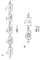
- Fig. 1 shows a block diagram of a representative data transmission system 100 employing duobinary signaling. More specifically, system 100 is designed to transmit information corresponding to an input binary data sequence, c k , e.g., a pseudo-random bit stream (PRBS), over a transmission channel 106. Sequence c k is recovered at the output of system 100 as sequence c' k . At the transmitter end, system 100 has a precoder 102 designed to introduce inter-symbol correlation (ISC) data into sequence c k .
- ISC inter-symbol correlation
- the resulting correlated binary sequence, p k is applied to a binary-to-duobinary (B/D) encoder 104, which generates a corresponding duobinary sequence, d k .
- B/D binary-to-duobinary
- Transmission channel 106 has a transmitter coupled to one end of a transmission link and an optional receiver coupled to the other end of that transmission link (none of which are explicitly shown in Fig. 1). Based on duobinary sequence d k , the transmitter generates an appropriate communication signal and applies that signal to the transmission link. At the remote end of the link, the receiver (if any) receives the communication signal and generates a corresponding analog signal denoted as s(t) in Fig. 1.
- channel 106 has (i) a transmitter comprising a laser coupled to an electro-optical modulator and (ii) a receiver comprising a photodiode, said transmitter and receiver coupled to an optical fiber.
- channel 106 has a radio-frequency (RF) transmitter and an RF receiver communicating over the wireless medium.
- channel 106 has an electrical waveform generator coupled to a conductor, e.g., a micro-strip line on a circuit board.
- Signal s(t) outputted by transmission channel 106 is applied to a D/B converter 108 to generate binary sequence p' k , which, with the exception of possible errors mostly due to imperfections in transmission channel 106, is identical to sequence p k .
- a decoder 110 reverses the coding of precoder 102 to generate sequence c' k . Decoder 110 may be designed to utilize the ISC of sequence p k to detect and correct errors in sequence p' k .
- a representative implementation of decoder 110 is described in U.S. Patent No. 4,086,566, the teachings of which are incorporated herein by reference.
- Fig. 2 shows a block diagram of a representative prior-art D/B converter 208, which can be used as D/B converter 108 in system 100.
- Converter 208 includes a full-wave rectifier (FWR) 212 coupled to a slicer 214.
- FWR 212 converts signal s(t) into rectified signal s'(t) , in which polarity of the negative waveforms is reversed while the positive waveforms remain substantially unchanged.
- Exemplary embodiments of FWR 212 can be found in U.S. Patent Nos. 4,941,080 and 6,480,405, the teachings of both of which are incorporated herein by reference.
- Slicer 214 then processes signal s'(t) as known in the art to produce sequence p' k .
- converter 208 is easily adapted to work at relatively low frequencies/bit rates, the same is not true for relatively high bit rates, e.g., about 10 Gb/s.
- relatively high bit rates e.g., about 10 Gb/s.
- parasitic circuit effects adversely affect the performance of the FWR and thereby converter 208.
- designing converter 208 that works well at relatively high bit rates and is also relatively small, power-efficient, and inexpensive may be difficult.
- Fig. 3 shows a block diagram of a D/B converter 308, which can be used as D/B converter 108 in system 100 according to one embodiment of the present invention.
- converter 308 performs relatively well at or above about 10 Gb/s and, at the same time, unlike prior-art converter 208 , may be smaller and less expensive to implement.
- converter 308 can be adapted in a relatively straightforward fashion to work at even higher bit rates and lends itself to relatively easy incorporation into an integrated device (e.g., an ASIC) for system 100.
- an integrated device e.g., an ASIC
- Signal s(t) applied to converter 308 is divided into two signal copies, s a (t) and s b (t) , using a wideband splitter 312 preferably having a bandwidth of about 1/2T b , where T b is the bit period of sequence c k .
- Copy s a (t) is applied to an inverting input of a first comparator 314a, whose non-inverting input receives a first threshold voltage, V 1 .
- copy s b (t) is applied to a non-inverting input of a second comparator 314b, whose inverting input receives a second threshold voltage, V 2 .
- the output, x , of each comparator 314 is a digital signal generated as follows.
- each comparator 314 is applied to an exclusive-OR (XOR) gate 316, which generates sequence p' k .
- XOR exclusive-OR
- Each of comparator 314a, comparator 314b, and XOR gate 316 preferably has a bandwidth of about 1/T b .
- Fig. 4 graphically illustrates one exemplary configuration of converter 308. More specifically, threshold voltages V 1 and V 2 are set at the values of about V 0 /2 and -V 0 /2, where V 0 is a voltage corresponding to the duobinary signal levels in signal copies s a (t) and s b (t) .
- the signal trace shown in Fig. 4 corresponds to a duobinary sequence of "+1, 0, -1".
- Table 2 illustrates the operation of converter 308 configured in accordance with Fig. 4.
- Exemplary Signal Values Generated in the Converter of Fig. 3 s a,b (t) x a x b p' k s a,b (t) ⁇ V 0 /2 0 1 1 -V 0 /2 ⁇ s a,b (t) ⁇ V 0 /2 1 1 0 s a,b (t) ⁇ -V 0 /2 1 0 1
- so configured converter 308 will correctly convert the signal shown in Fig. 4 into a binary sequence of "101".
- Fig. 5 shows a block diagram of a D/B converter 508, which can be used as D/B converter 108 in system 100 according to another embodiment of the present invention.
- Converter 508 is similar to converter 308 (Fig. 3) and includes a wideband splitter 512, two comparators 514a-b, and a logic gate 516 .
- one difference between converters 508 and 308 is that, in converter 508 , each signal copy is applied to a non-inverting input of the corresponding comparator 514 .
- logic gate 516 is an exclusive-NOR (XNOR) gate.
- Table 3 illustrates the operation of converter 508 configured in accordance with Fig. 4.
- Exemplary Signal Values Generated in the Converter of Fig. 5 s a,b (t) x a x b p' k s a,b (t) > V 0 /2 1 1 1 - V 0 /2 ⁇ s a,b (t) ⁇ V 0 /2 0 1 0 s a,b (t) ⁇ -V 0 /2 0 0 1
- converter 508 will correctly convert the signal shown in Fig. 4 to generate the "101" sequence.
- converters of the present invention adapted for relatively high bit rates do not require complex microwave-matching circuits of prior-art converters (e.g., converter 208 of Fig. 2).
- the inventors' own research demonstrated that a converter of the invention embodied in an indium-phosphate-based integrated circuit (i) was robust and relatively inexpensive and (ii) performed relatively well with bit rates as high as 40 Gb/s.
- converters of the present invention are described as receiving analog signals, they can similarly be configured to receive digital signals.
- Data sequences may be represented by non-return-to-zero (NRZ) or return-to-zero (RZ) signals.
- a converter of the invention may be based on a pair of comparators whose configuration may be differently and appropriately selected.
- a logic gate may be implemented as a combination of suitable logic elements as known in the art. For example, XNOR gate 516 (Fig. 5) may be implemented as an XOR gate followed by an inverter.
- Transmission system employing a converter of the invention may be configured to operate with or without data precoding and the corresponding decoding.
- exemplary data rates e.g., 10 Gb/s
- converters of the invention may similarly be designed to operate at other selected bit rates.
Landscapes
- Engineering & Computer Science (AREA)
- Theoretical Computer Science (AREA)
- Dc Digital Transmission (AREA)
Abstract
A duobinary-to-binary signal converter includes a pair of comparators
coupled to a logic gate. Each comparator receives a copy of a duobinary-encoded analog signal
applied to the converter and is designed to generate a binary output based on the comparison of the
magnitude of the received signal with a corresponding threshold voltage. The outputs of the
comparators are fed into the logic gate, which generates a binary sequence corresponding to the
duobinary-encoded signal. A representative converter of the invention can perform relatively well
at bit rates as high as about 40 Gb/s and can be conveniently incorporated into an appropriate
integrated device (e.g., an ASIC) for a data transmission system employing duobinary signaling.
Description
- The present invention relates to communication equipment and, more specifically, to equipment for decoding duobinary signals.
- Duobinary signaling was introduced in the 1960s and since then has found numerous applications in communication systems. The principle of duobinary signaling is explained, for example, in an article by A. Lender that appeared in IEEE Transactions on Communications and Electronics, Vol. 82 (May, 1963), pp. 214-218, the teachings of which are incorporated herein by reference. Briefly, duobinary signaling uses three signal levels, for example, "+1", "0", and "-1". A signal corresponding to one of these levels (i.e., a duobinary symbol) is transmitted during each signaling interval (time slot). A duobinary signal is typically generated from a corresponding binary signal using certain transformation rules. Although both signals carry the same information, the bandwidth of the duobinary signal may be reduced by a factor of 2 compared to that of the binary signal at the expense of signal-to-noise ratio. In addition, the duobinary signal may be constructed such that it has certain inter-symbol correlation (ISC) data, which can be used to implement an error-correction algorithm at the receiver.
- A number of different transformations have been proposed for constructing a duobinary sequence, bk , from a corresponding binary sequence, ak , where k = 1, 2, 3, ... One such transformation described in the above-cited Lender article is as follows. For any particular k = m, when am = 0, bm = 0. When am = 1, bm equals either +1 or -1, with the polarity of bm determined based on the polarity of last non-zero symbol bm-i preceding bm , where i is a positive integer. More specifically, when i is odd, the polarity of bm is the same as the polarity of bm-i ; and, when i is even, the polarity of bm is the opposite of the polarity of bm-i . Due to the properties of this transformation, the duobinary sequence has no transitions between the "+1" and "-1" levels in successive time slots. Only transitions between (i) "0" and "+1" and (ii) "0" and "-1" levels can occur. Reconstruction of ak from a known bk is relatively straightforward. More specifically, when bm = ±1, am = 1; and, when bm = 0, am = 0.
- Table 1 reproduces an example given in the Lender article to further illustrate the above-described transformation.

- A duobinary-to-binary (D/B) signal converter is a device that is used at the receiver end of a data transmission system to reconstruct a binary sequence from a corresponding duobinary-encoded signal. A typical prior-art D/B converter is implemented using a full-wave rectifier as described in more detail below. However, one problem with such a converter is that, at relatively high data transmission rates, e.g., when the physical size of the circuit is comparable to the wavelength corresponding to the data rate, its performance becomes adversely affected. For the current level of technology, such a problem occurs at data rates of about 10 Gb/s.
- Problems in the prior art are addressed, in accordance with the principles of the present invention, by a duobinary-to-binary signal converter including, in one embodiment, a pair of comparators coupled to a logic gate. Each comparator receives a copy of a duobinary-encoded analog signal applied to the converter and is designed to generate a binary output based on the comparison of the magnitude of the received signal with a corresponding threshold voltage. The outputs of the comparators are fed into the logic gate, which generates a binary sequence corresponding to the duobinary-encoded signal. A representative converter of the invention can perform relatively well at bit rates as high as about 40 Gb/s and can be conveniently incorporated into an appropriate integrated device (e.g., an ASIC) for a data transmission system employing duobinary signaling.
- According to one embodiment, the present invention is a device, comprising: a first comparator adapted to receive a first copy of an input signal and generate a first binary signal; a second comparator adapted to receive a second copy of the input signal and generate a second binary signal; and a logic gate adapted to generate a third binary signal based on the first and second binary signals, wherein: the input signal corresponds to a duobinary sequence; and the third binary signal is a binary representation of the duobinary sequence.
- According to another embodiment, the present invention is a method of signal processing, comprising: (A) comparing magnitude of an electrical signal with first and second threshold voltages to generate first and second binary values; (B) applying a logic function to the first and second binary values to generate a third binary value; and (C) repeating steps (A) and (B) to generate a sequence of third binary values, wherein: the electrical signal corresponds to a duobinary sequence; and the sequence of third values is a binary representation of the duobinary sequence.
- According to yet another embodiment, the present invention is a data transmission system designed to use duobinary signaling, the system including a device comprising: a first comparator adapted to receive a first copy of an input signal and generate a first binary signal; a second comparator adapted to receive a second copy of the input signal and generate a second binary signal; and a logic gate adapted to generate a third binary signal based on the first and second binary signals, wherein: the input signal corresponds to a duobinary sequence; and the third binary signal is a binary representation of the duobinary sequence.
- Other aspects, features, and benefits of the present invention will become more fully apparent from the following detailed description, the appended claims, and the accompanying drawings in which:
- Fig. 1 shows a block diagram of a representative data transmission system employing duobinary signaling;
- Fig. 2 shows a block diagram of a representative prior-art D/B converter that can be used in the system of Fig. 1;
- Fig. 3 shows a block diagram of a D/B converter that can be used in the system of Fig. 1 according to one embodiment of the present invention;
- Fig. 4 graphically illustrates one exemplary configuration of the D/B converter of Fig. 3; and
- Fig. 5 shows a block diagram of a D/B converter that can be used in the system of Fig. 1 according to another embodiment of the present invention.
-
- Reference herein to "one embodiment" or "an embodiment" means that a particular feature, structure, or characteristic described in connection with the embodiment can be included in at least one embodiment of the invention. The appearances of the phrase "in one embodiment" in various places in the specification are not necessarily all referring to the same embodiment, nor are separate or alternative embodiments mutually exclusive of other embodiments.
- Fig. 1 shows a block diagram of a representative
data transmission system 100 employing duobinary signaling. More specifically,system 100 is designed to transmit information corresponding to an input binary data sequence, ck , e.g., a pseudo-random bit stream (PRBS), over atransmission channel 106. Sequence ck is recovered at the output ofsystem 100 as sequence c'k . At the transmitter end,system 100 has aprecoder 102 designed to introduce inter-symbol correlation (ISC) data into sequence ck . The resulting correlated binary sequence, pk , is applied to a binary-to-duobinary (B/D)encoder 104, which generates a corresponding duobinary sequence, dk . More details on representative circuits that can serve asprecoder 102 andencoder 104 insystem 100 can be found, for example, in U.S. Patent No. 5,892,858, the teachings of which are incorporated herein by reference. -
Transmission channel 106 has a transmitter coupled to one end of a transmission link and an optional receiver coupled to the other end of that transmission link (none of which are explicitly shown in Fig. 1). Based on duobinary sequence dk , the transmitter generates an appropriate communication signal and applies that signal to the transmission link. At the remote end of the link, the receiver (if any) receives the communication signal and generates a corresponding analog signal denoted as s(t) in Fig. 1. In one embodiment,channel 106 has (i) a transmitter comprising a laser coupled to an electro-optical modulator and (ii) a receiver comprising a photodiode, said transmitter and receiver coupled to an optical fiber. In another embodiment,channel 106 has a radio-frequency (RF) transmitter and an RF receiver communicating over the wireless medium. In yet another embodiment,channel 106 has an electrical waveform generator coupled to a conductor, e.g., a micro-strip line on a circuit board. - Signal s(t) outputted by
transmission channel 106 is applied to a D/B converter 108 to generate binary sequence p'k , which, with the exception of possible errors mostly due to imperfections intransmission channel 106, is identical to sequence pk . Adecoder 110 reverses the coding ofprecoder 102 to generate sequence c'k .Decoder 110 may be designed to utilize the ISC of sequence pk to detect and correct errors in sequence p'k . A representative implementation ofdecoder 110 is described in U.S. Patent No. 4,086,566, the teachings of which are incorporated herein by reference. - Fig. 2 shows a block diagram of a representative prior-art D/
B converter 208, which can be used as D/B converter 108 insystem 100.Converter 208 includes a full-wave rectifier (FWR) 212 coupled to a slicer 214.FWR 212 converts signal s(t) into rectified signal s'(t), in which polarity of the negative waveforms is reversed while the positive waveforms remain substantially unchanged. Exemplary embodiments of FWR 212 can be found in U.S. Patent Nos. 4,941,080 and 6,480,405, the teachings of both of which are incorporated herein by reference. Slicer 214 then processes signal s'(t) as known in the art to produce sequence p'k . - Although
converter 208 is easily adapted to work at relatively low frequencies/bit rates, the same is not true for relatively high bit rates, e.g., about 10 Gb/s. In particular, when the wavelength of RF signals inFWR 212 is comparable to certain circuit dimensions, parasitic circuit effects adversely affect the performance of the FWR and thereby converter 208. As a result, designingconverter 208 that works well at relatively high bit rates and is also relatively small, power-efficient, and inexpensive may be difficult. - Fig. 3 shows a block diagram of a D/
B converter 308, which can be used as D/B converter 108 insystem 100 according to one embodiment of the present invention. As will be understood by one skilled in the art from the provided description,converter 308 performs relatively well at or above about 10 Gb/s and, at the same time, unlike prior-art converter 208, may be smaller and less expensive to implement. In addition,converter 308 can be adapted in a relatively straightforward fashion to work at even higher bit rates and lends itself to relatively easy incorporation into an integrated device (e.g., an ASIC) forsystem 100. - Signal s(t) applied to
converter 308 is divided into two signal copies, sa(t) and sb(t), using awideband splitter 312 preferably having a bandwidth of about 1/2Tb, where Tb is the bit period of sequence ck . Copy sa(t) is applied to an inverting input of afirst comparator 314a, whose non-inverting input receives a first threshold voltage, V1. Similarly, copy sb(t) is applied to a non-inverting input of asecond comparator 314b, whose inverting input receives a second threshold voltage, V2. The output, x, of each comparator 314 is a digital signal generated as follows. When V- ≥ V+, x = 0; and, when V- < V+, x = 1, where V- and V+ are the voltages applied to the inverting and non-inverting inputs, respectively, of the comparator. The output of each comparator 314 is applied to an exclusive-OR (XOR)gate 316, which generates sequence p'k . Each ofcomparator 314a,comparator 314b, andXOR gate 316 preferably has a bandwidth of about 1/Tb. - Fig. 4 graphically illustrates one exemplary configuration of
converter 308. More specifically, threshold voltages V1 and V2 are set at the values of about V0/2 and -V0/2, where V0 is a voltage corresponding to the duobinary signal levels in signal copies sa(t) and sb(t). The signal trace shown in Fig. 4 corresponds to a duobinary sequence of "+1, 0, -1". - Table 2 illustrates the operation of
converter 308 configured in accordance with Fig. 4.Exemplary Signal Values Generated in the Converter of Fig. 3 sa,b(t) xa xb p'k sa,b(t) ≥ V0/2 0 1 1 -V0/2 ≤ sa,b(t) < V0/2 1 1 0 sa,b(t) < -V0/2 1 0 1 converter 308 will correctly convert the signal shown in Fig. 4 into a binary sequence of "101". - Fig. 5 shows a block diagram of a D/
B converter 508, which can be used as D/B converter 108 insystem 100 according to another embodiment of the present invention.Converter 508 is similar to converter 308 (Fig. 3) and includes awideband splitter 512, twocomparators 514a-b, and alogic gate 516. However, one difference betweenconverters converter 508, each signal copy is applied to a non-inverting input of the corresponding comparator 514. Another difference between said converters is thatlogic gate 516 is an exclusive-NOR (XNOR) gate. - Table 3 illustrates the operation of
converter 508 configured in accordance with Fig. 4.Exemplary Signal Values Generated in the Converter of Fig. 5 sa,b(t) xa xb p'k sa,b(t) > V0/2 1 1 1 - V0/2 ≤ sa,b(t) ≤ V0/2 0 1 0 sa,b(t) < -V0/2 0 0 1 converter 308,converter 508 will correctly convert the signal shown in Fig. 4 to generate the "101" sequence. - Advantageously, converters of the present invention adapted for relatively high bit rates do not require complex microwave-matching circuits of prior-art converters (e.g.,
converter 208 of Fig. 2). Furthermore, the inventors' own research demonstrated that a converter of the invention embodied in an indium-phosphate-based integrated circuit (i) was robust and relatively inexpensive and (ii) performed relatively well with bit rates as high as 40 Gb/s. - While this invention has been described with reference to illustrative embodiments, this description is not intended to be construed in a limiting sense. Although converters of the present invention are described as receiving analog signals, they can similarly be configured to receive digital signals. Data sequences may be represented by non-return-to-zero (NRZ) or return-to-zero (RZ) signals. A converter of the invention may be based on a pair of comparators whose configuration may be differently and appropriately selected. A logic gate may be implemented as a combination of suitable logic elements as known in the art. For example, XNOR gate 516 (Fig. 5) may be implemented as an XOR gate followed by an inverter. Transmission system employing a converter of the invention may be configured to operate with or without data precoding and the corresponding decoding. Although exemplary data rates (e.g., 10 Gb/s) were used in the above description, converters of the invention may similarly be designed to operate at other selected bit rates. Various modifications of the described embodiments, as well as other embodiments of the invention, which are apparent to persons skilled in the art to which the invention pertains are deemed to lie within the principle and scope of the invention as expressed in the following claims.
- Although the steps in the following method claims, if any, are recited in a particular sequence with corresponding labeling, unless the claim recitations otherwise imply a particular sequence for implementing some or all of those steps, those steps are not necessarily intended to be limited to being implemented in that particular sequence.
Claims (10)
- A device, comprising:a first comparator adapted to receive a first copy of an input signal and generate a first binary signal;a second comparator adapted to receive a second copy of the input signal and generate a second binary signal; anda logic gate adapted to generate a third binary signal based on the first and second binary signals, wherein:the input signal corresponds to a duobinary sequence; andthe third binary signal is a binary representation of the duobinary sequence.
- The device of claim 1, wherein:the input signal is an analog signal;the logic gate comprises an exclusive-OR gate; andthe input signal corresponds to a bit rate of higher than about 10 Gb/s.
- The device of claim 1, further comprising a splitter adapted to receive the input signal and generate the first and second copies, wherein:the splitter has a bandwidth of about 1/2Tb, where Tb is a bit period corresponding to the input signal; andeach of the first and second comparators and the logic gate has a bandwidth of about 1/Tb.
- The device of claim 1, wherein:for each comparator,
when voltage applied to a first input port is equal to or higher than voltage applied to a second input port, the corresponding binary signal has binary "0"; and
when the voltage applied to the first input port is lower than the voltage applied to the second input port, the corresponding binary signal has binary "1". - The device of claim 4, wherein:for the first comparator,
the first copy is applied to the first input port; and
a first threshold voltage is applied to the second input port; andfor the second comparator,
a second threshold voltage is applied to the first input port; and
the second copy is applied to the second input port. - The device of claim 4, wherein:for each comparator,
a corresponding threshold voltage is applied to the first input port; and
the corresponding signal copy is applied to the second input port. - A method of signal processing, comprising:(A) comparing magnitude of an electrical signal with first and second threshold voltages to generate first and second binary values;(B) applying a logic function to the first and second binary values to generate a third binary value; and(C) repeating steps (A) and (B) to generate a sequence of third binary values, wherein:the electrical signal corresponds to a duobinary sequence; andthe sequence of third values is a binary representation of the duobinary sequence.
- The method of claim 7, wherein, for step (A):for each threshold voltage,
when the magnitude of the electrical signal is equal to or higher than the threshold voltage, the corresponding binary value is "0"; and
when the magnitude of the electrical signal is lower than the threshold voltage, the corresponding binary value is "1". - The method of claim 7, wherein, for step (A):when the magnitude of the electrical signal is equal to or higher than the first threshold voltage, the first binary value is "0";when the magnitude of the electrical signal is lower than the first threshold voltage, the first binary value is "1";when the magnitude of the electrical signal is equal to or lower than the second threshold voltage, the second binary value is "0"; andwhen the magnitude of the electrical signal is higher than the second threshold voltage, the second binary value is "1".
- A data transmission system designed to use duobinary signaling, the system including a device comprising:a first comparator adapted to receive a first copy of an input signal and generate a first binary signal;a second comparator adapted to receive a second copy of the input signal and generate a second binary signal; anda logic gate adapted to generate a third binary signal based on the first and second binary signals, wherein:the input signal corresponds to a duobinary sequence; andthe third binary signal is a binary representation of the duobinary sequence.
Applications Claiming Priority (2)
| Application Number | Priority Date | Filing Date | Title |
|---|---|---|---|
| US630422 | 1996-04-02 | ||
| US10/630,422 US20050024253A1 (en) | 2003-07-30 | 2003-07-30 | Duobinary-to-binary signal converter |
Publications (1)
| Publication Number | Publication Date |
|---|---|
| EP1503501A1 true EP1503501A1 (en) | 2005-02-02 |
Family
ID=33541497
Family Applications (1)
| Application Number | Title | Priority Date | Filing Date |
|---|---|---|---|
| EP04254284A Withdrawn EP1503501A1 (en) | 2003-07-30 | 2004-07-16 | Duobinary to binary decoder |
Country Status (4)
| Country | Link |
|---|---|
| US (1) | US20050024253A1 (en) |
| EP (1) | EP1503501A1 (en) |
| JP (1) | JP2005051789A (en) |
| CN (1) | CN1585280A (en) |
Cited By (3)
| Publication number | Priority date | Publication date | Assignee | Title |
|---|---|---|---|---|
| EP2843854A1 (en) * | 2013-08-27 | 2015-03-04 | ADVA Optical Networking SE | Method, transmitter and receiver device for transmitting a binary digital transmit signal over an optical transmission link |
| EP2913928A1 (en) * | 2014-02-27 | 2015-09-02 | Alcatel Lucent | Circuitry and method for converting a multi-level signal into at least one binary signal |
| EP2913927A1 (en) * | 2014-02-27 | 2015-09-02 | Alcatel Lucent | Circuitry and method for multi-level signals |
Families Citing this family (10)
| Publication number | Priority date | Publication date | Assignee | Title |
|---|---|---|---|---|
| US7508882B2 (en) * | 2003-12-04 | 2009-03-24 | Alcatel-Lucent Usa Inc. | Electrical backplane transmission using duobinary signaling |
| WO2007037312A1 (en) * | 2005-09-28 | 2007-04-05 | Nec Corporation | Clock reproduction device and method |
| CN102202245B (en) * | 2010-03-23 | 2013-09-11 | 华为技术有限公司 | Method, device and system for processing signals |
| US10086442B2 (en) | 2012-07-17 | 2018-10-02 | Weihai Dawang Hardware Products Limited | Drill chuck |
| US9049094B2 (en) | 2012-11-13 | 2015-06-02 | Alcatel Lucent | Generation of multilevel signals using correlative coding |
| FR3090113B1 (en) * | 2018-12-14 | 2020-12-04 | Aptiv Tech Ltd | Device and method for self-adjusting an electrical threshold for detecting a power fault. |
| CN113924738B (en) * | 2019-04-12 | 2024-12-03 | 迈凌有限公司 | Electrically dual binary soft information receiver for NRZ modulated optical fiber transmission |
| WO2021176576A1 (en) * | 2020-03-03 | 2021-09-10 | 三菱電機株式会社 | Unsteadiness detection system, unsteadiness detection method, and unsteadiness detection program |
| KR102995533B1 (en) * | 2020-04-29 | 2026-07-24 | 삼성전자주식회사 | Data transceiving system including clock and data recovery device and operating method thereof |
| DE112024003020T5 (en) * | 2023-07-19 | 2026-06-18 | Maxlinear, Inc. | Optical receiver with soft-decision processing and low complexity |
Citations (3)
| Publication number | Priority date | Publication date | Assignee | Title |
|---|---|---|---|---|
| GB2217957A (en) * | 1988-04-27 | 1989-11-01 | Philips Electronic Associated | Circuit arrangement for producing a binary signal |
| EP0369159A2 (en) * | 1988-11-15 | 1990-05-23 | ANT Nachrichtentechnik GmbH | Method for the restitution of binary information from a basic band signal showing faults, and arrangement |
| EP0551858A2 (en) * | 1992-01-15 | 1993-07-21 | Samsung Electronics Co., Ltd. | Duobinary to binary decoder |
Family Cites Families (8)
| Publication number | Priority date | Publication date | Assignee | Title |
|---|---|---|---|---|
| US3866147A (en) * | 1973-02-26 | 1975-02-11 | Univ Sherbrooke | Balanced correlated ternary coding system |
| US4086566A (en) * | 1976-11-15 | 1978-04-25 | Gte Automatic Electric Laboratories Incorporated | Error detector for modified duobinary signals |
| FR2612025B1 (en) * | 1987-03-06 | 1989-05-26 | Labo Electronique Physique | DUOBINARY CODED SIGNAL DECODING DEVICE |
| DE3831454A1 (en) * | 1988-09-16 | 1990-03-29 | Philips Patentverwaltung | FULL-WAY RECTIFIER SWITCHING |
| US5544323A (en) * | 1993-09-23 | 1996-08-06 | Standard Microsystems Corp. | High bit rate ethernet connection |
| US5640605A (en) * | 1994-08-26 | 1997-06-17 | 3Com Corporation | Method and apparatus for synchronized transmission of data between a network adaptor and multiple transmission channels using a shared clocking frequency and multilevel data encoding |
| US5892858A (en) * | 1997-03-27 | 1999-04-06 | Northern Telecom Limited | Duobinary coding and modulation technique for optical communication systems |
| US6480405B2 (en) * | 2000-11-17 | 2002-11-12 | Texas Instruments Incorporated | Full-wave rectifier |
-
2003
- 2003-07-30 US US10/630,422 patent/US20050024253A1/en not_active Abandoned
-
2004
- 2004-07-16 EP EP04254284A patent/EP1503501A1/en not_active Withdrawn
- 2004-07-29 CN CNA2004100590503A patent/CN1585280A/en active Pending
- 2004-07-30 JP JP2004222681A patent/JP2005051789A/en active Pending
Patent Citations (3)
| Publication number | Priority date | Publication date | Assignee | Title |
|---|---|---|---|---|
| GB2217957A (en) * | 1988-04-27 | 1989-11-01 | Philips Electronic Associated | Circuit arrangement for producing a binary signal |
| EP0369159A2 (en) * | 1988-11-15 | 1990-05-23 | ANT Nachrichtentechnik GmbH | Method for the restitution of binary information from a basic band signal showing faults, and arrangement |
| EP0551858A2 (en) * | 1992-01-15 | 1993-07-21 | Samsung Electronics Co., Ltd. | Duobinary to binary decoder |
Non-Patent Citations (1)
| Title |
|---|
| MAY G ET AL: "EXTENDED 10 GB/S FIBER TRANSMISSION DISTANCE AT 1538 NM USING A DUOBINARY RECEIVER", IEEE PHOTONICS TECHNOLOGY LETTERS, IEEE INC. NEW YORK, US, vol. 6, no. 5, 1 May 1994 (1994-05-01), pages 648 - 650, XP000446985, ISSN: 1041-1135 * |
Cited By (6)
| Publication number | Priority date | Publication date | Assignee | Title |
|---|---|---|---|---|
| EP2843854A1 (en) * | 2013-08-27 | 2015-03-04 | ADVA Optical Networking SE | Method, transmitter and receiver device for transmitting a binary digital transmit signal over an optical transmission link |
| US9215116B2 (en) | 2013-08-27 | 2015-12-15 | Adva Optical Networking Se | Method, transmitter and receiver device for transmitting a binary digital transmit signal over an optical transmission link |
| EP2913928A1 (en) * | 2014-02-27 | 2015-09-02 | Alcatel Lucent | Circuitry and method for converting a multi-level signal into at least one binary signal |
| EP2913927A1 (en) * | 2014-02-27 | 2015-09-02 | Alcatel Lucent | Circuitry and method for multi-level signals |
| WO2015128274A1 (en) * | 2014-02-27 | 2015-09-03 | Alcatel Lucent | Circuitry and method for converting a multi-level signal into at least one binary signal |
| US9369317B2 (en) | 2014-02-27 | 2016-06-14 | Imec Vzw | Circuitry and method for multi-level signals |
Also Published As
| Publication number | Publication date |
|---|---|
| JP2005051789A (en) | 2005-02-24 |
| US20050024253A1 (en) | 2005-02-03 |
| CN1585280A (en) | 2005-02-23 |
Similar Documents
| Publication | Publication Date | Title |
|---|---|---|
| US7180957B2 (en) | Technique for utilizing spare bandwidth resulting from the use of a transition-limiting code in a multi-level signaling system | |
| US7224737B2 (en) | Method and apparatus employing PAM-5 coding with clock embedded in data stream and having a transition when data bits remain unchanged | |
| US20060126751A1 (en) | Technique for disparity bounding coding in a multi-level signaling system | |
| JPH11512277A (en) | Duobinary coding and modulation technology for optical communication systems | |
| US20050024253A1 (en) | Duobinary-to-binary signal converter | |
| US8416840B2 (en) | Duobinary transceiver | |
| US7643761B2 (en) | Method and apparatus for processing optical duobinary signals | |
| KR20000031961A (en) | Encoder/decorder of bit insertion modulation path code for high-speed optical transmission system | |
| US7508882B2 (en) | Electrical backplane transmission using duobinary signaling | |
| US6804472B1 (en) | Transmitter and method using half rate data streams for generating full rate modulation on an optical signal | |
| US20050259772A1 (en) | Circuit arrangement and method to provide error detection for multi-level analog signals, including 3-level pulse amplitude modulation (PAM-3) signals | |
| CN1627667B (en) | Duobinary receiver | |
| US6263465B1 (en) | Error detection and correction in systems receiving NRZ signals from transmission of RZ signals | |
| US7260151B2 (en) | Dual phase pulse modulation system | |
| US7349471B2 (en) | PPM receiving system and method using time-interleaved integrators | |
| JP3085275B2 (en) | Binary optical transmission method and binary optical transmission system | |
| JP3664953B2 (en) | Semiconductor integrated circuit device | |
| EP3954068B1 (en) | Encoding and decoding communications traffic in a pulse amplitude modulation format and optical apparatus for same | |
| CN112350967A (en) | HDB3 encoding and decoding methods and devices | |
| US20150244547A1 (en) | Circuitry and Method for Multi-Level Signals | |
| JP2005080144A (en) | Data modulation / demodulation method for serial transmission device | |
| Alyaei et al. | Line coded modulation | |
| WO2022100860A1 (en) | Detecting intensity modulated optical signal by low bandwidth receiving device | |
| CN115208366A (en) | Duobinary four-level pulse amplitude modulation signal processing method and system | |
| US20060165194A1 (en) | Data sending device, data receiving device, and data transmission method |
Legal Events
| Date | Code | Title | Description |
|---|---|---|---|
| PUAI | Public reference made under article 153(3) epc to a published international application that has entered the european phase |
Free format text: ORIGINAL CODE: 0009012 |
|
| 17P | Request for examination filed |
Effective date: 20040807 |
|
| AK | Designated contracting states |
Kind code of ref document: A1 Designated state(s): AT BE BG CH CY CZ DE DK EE ES FI FR GB GR HU IE IT LI LU MC NL PL PT RO SE SI SK TR |
|
| AX | Request for extension of the european patent |
Extension state: AL HR LT LV MK |
|
| AKX | Designation fees paid |
Designated state(s): DE FR GB |
|
| STAA | Information on the status of an ep patent application or granted ep patent |
Free format text: STATUS: THE APPLICATION HAS BEEN WITHDRAWN |
|
| 18W | Application withdrawn |
Effective date: 20051026 |