EP1501020A1 - A non-volatile memory parallel processor - Google Patents
A non-volatile memory parallel processor Download PDFInfo
- Publication number
- EP1501020A1 EP1501020A1 EP04253575A EP04253575A EP1501020A1 EP 1501020 A1 EP1501020 A1 EP 1501020A1 EP 04253575 A EP04253575 A EP 04253575A EP 04253575 A EP04253575 A EP 04253575A EP 1501020 A1 EP1501020 A1 EP 1501020A1
- Authority
- EP
- European Patent Office
- Prior art keywords
- processor
- memory cell
- mram
- volatile memory
- cell
- Prior art date
- Legal status (The legal status is an assumption and is not a legal conclusion. Google has not performed a legal analysis and makes no representation as to the accuracy of the status listed.)
- Withdrawn
Links
Images





Classifications
-
- B—PERFORMING OPERATIONS; TRANSPORTING
- B82—NANOTECHNOLOGY
- B82Y—SPECIFIC USES OR APPLICATIONS OF NANOSTRUCTURES; MEASUREMENT OR ANALYSIS OF NANOSTRUCTURES; MANUFACTURE OR TREATMENT OF NANOSTRUCTURES
- B82Y10/00—Nanotechnology for information processing, storage or transmission, e.g. quantum computing or single electron logic
-
- G—PHYSICS
- G06—COMPUTING OR CALCULATING; COUNTING
- G06F—ELECTRIC DIGITAL DATA PROCESSING
- G06F15/00—Digital computers in general; Data processing equipment in general
- G06F15/76—Architectures of general purpose stored program computers
- G06F15/80—Architectures of general purpose stored program computers comprising an array of processing units with common control, e.g. single instruction multiple data processors
- G06F15/8007—Architectures of general purpose stored program computers comprising an array of processing units with common control, e.g. single instruction multiple data processors single instruction multiple data [SIMD] multiprocessors
-
- G—PHYSICS
- G11—INFORMATION STORAGE
- G11C—STATIC STORES
- G11C14/00—Digital stores characterised by arrangements of cells having volatile and non-volatile storage properties for back-up when the power is down
- G11C14/0009—Digital stores characterised by arrangements of cells having volatile and non-volatile storage properties for back-up when the power is down in which the volatile element is a DRAM cell
- G11C14/0036—Digital stores characterised by arrangements of cells having volatile and non-volatile storage properties for back-up when the power is down in which the volatile element is a DRAM cell and the nonvolatile element is a magnetic RAM [MRAM] element or ferromagnetic cell
-
- G—PHYSICS
- G11—INFORMATION STORAGE
- G11C—STATIC STORES
- G11C7/00—Arrangements for writing information into, or reading information out from, a digital store
- G11C7/10—Input/output [I/O] data interface arrangements, e.g. I/O data control circuits, I/O data buffers
- G11C7/1006—Data managing, e.g. manipulating data before writing or reading out, data bus switches or control circuits therefor
-
- H—ELECTRICITY
- H10—SEMICONDUCTOR DEVICES; ELECTRIC SOLID-STATE DEVICES NOT OTHERWISE PROVIDED FOR
- H10B—ELECTRONIC MEMORY DEVICES
- H10B12/00—Dynamic random access memory [DRAM] devices
- H10B12/50—Peripheral circuit region structures
-
- H—ELECTRICITY
- H10—SEMICONDUCTOR DEVICES; ELECTRIC SOLID-STATE DEVICES NOT OTHERWISE PROVIDED FOR
- H10B—ELECTRONIC MEMORY DEVICES
- H10B61/00—Magnetic memory devices, e.g. magnetoresistive RAM [MRAM] devices
- H10B61/20—Magnetic memory devices, e.g. magnetoresistive RAM [MRAM] devices comprising components having three or more electrodes, e.g. transistors
- H10B61/22—Magnetic memory devices, e.g. magnetoresistive RAM [MRAM] devices comprising components having three or more electrodes, e.g. transistors of the field-effect transistor [FET] type
Definitions
- the invention relates generally to electronic memory. More particularly, the invention relates to a non-volatile memory parallel processor.
- Computer systems are becoming increasingly sophisticated allowing users to perform a continually increasing variety of computing tasks at faster rates. As a result, complex computations are required to be performed by the computer systems at greater rates.
- Parallel processing is a method in which multiple operations or computations are performed in parallel. That is, instead of performing the operations serially, the operations are performed simultaneously. The results of the simultaneous operations can be combined after being individually completed. The net result is that total computations can be performed at greater speeds.
- Parallel processing can be particularly useful for applications that receive or generate a large number of inputs or outputs, and provide processing of the inputs and outputs. For example, the reception or generation of images can benefit from parallel processing.
- Image processing can include operations being performed on many image elements (for example, pixels).
- parallel processing computing systems are typically volatile. That is, generally the parallel processing computing systems fail if power to the computing systems is turned off. In some applications, this reduces the efficiency of the computing system. It can be advantageous to be able to maintain the parallel processing data during a power shut down, so that the processing can be easily restarted.
- the present invention seeks to provide an improved parallel processor.
- the preferred embodiment provides apparatus and a method of parallel processing that is non-volatile, that is adaptable for image processing and/or which is easily integratable.
- the invention includes an apparatus and method for parallel processing.
- the apparatus and method are adaptable for image processing. Additionally, the parallel processing apparatus can be efficiently integrated.
- An embodiment of the invention includes a parallel processor.
- the parallel processor includes a plurality of non-volatile memory cells.
- the parallel processor additionally includes a plurality of processor elements. At least one non-volatile memory cell corresponds with each of the processor elements.
- the processor elements each access data from at least one corresponding non-volatile memory cell.
- the processor elements perform processing on the data.
- the non-volatile memory cells can include magnetic memory.
- the described embodiments provide apparatus for and a method of parallel processing data stored in MRAM elements with multiple processor elements.
- the parallel processing apparatus can be efficiently integrated.
- Figure 1 shows an embodiment of the invention. More specifically, the embodiment of Figure 1 includes a parallel processor.
- the parallel processor includes a plurality of non-volatile memory cells 110, 112, 114, 116. Additionally, the parallel processor includes a plurality of processor elements 120, 122, 124, 126. As shown in Figure 1, at least one non-volatile memory cell 110, 112, 114, 116 corresponds with each of the processor elements 120, 122, 124, 126.
- the processor elements 120, 122, 124, 126 can each access data from an at least one corresponding non-volatile memory cell 110, 112, 114, 116.
- the processor elements 120, 122, 124, 126 can process data that has been stored in the non-volatile memory cell 110, 112, 114, 116.
- Control and data lines 140, 141, 142, 143 are included within Figure 1 to depict that in some embodiments, the processor elements 120, 122, 124, 126 can access data from more non-volatile memory cells 110, 112, 114, 116 than just the corresponding non-volatile memory cell 110, 112, 114, 116.
- non-volatile memory cell 110, 112, 114, 116 The data stored in the non-volatile memory cell 110, 112, 114, 116 is retained when power to the parallel processor is turned off. Therefore, a system implementing the parallel processor of Figure 1 can quickly recover after power is restored. Additionally, some types of non-volatile memory, such as magnetic memory, can provide quick access times, which can improve system performance.
- the non-volatile memory cells 110, 112, 114, 116 can be integrated with the processor elements 120, 122, 124, 126.
- the non-volatile memory cells 110, 112, 114, 116 can be magnetic memory cells.
- An embodiment includes each magnetic memory cell 110, 112, 114, 116 being formed adjacent to a substrate, and the corresponding processor 120, 122, 124, 126 element being formed in the substrate adjacent to the magnetic memory cell.
- an embodiment includes each non-volatile memory cell being interfaced with a corresponding at least one dynamic random access memory (DRAM) cell.
- DRAM dynamic random access memory
- the embodiment of Figure 1 includes a master processor 130.
- the master processor can combine processed data from each of the processor elements 120, 122, 124, 126.
- the configuration can provide advantages over a single processor configuration because each of the processor elements 120, 122, 124, 126 can process data in parallel.
- Another configuration does not include the master processor 130, but rather, includes at least one of the processor elements 120, 122, 124, 126 providing the functionality of the master processor. Additionally, the processor elements 120, 122, 124, 126 providing the master processor functionality can change over time.
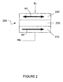
- FIG. 2 shows a magnetic memory cell (MRAM) 200 according to an embodiment of the invention.
- the MRAM memory cell 200 includes a sense layer 220, a dielectric region 230 and a reference layer 210.
- the orientation of magnetization within the sense layer 220 is non-fixed, and can assume two stable orientations as shown by the arrow M1.
- the reference layer 210 (also referred to as a pinned magnetic region) has a fixed magnetic orientation as depicted by the arrow M2.
- the dielectric region 230 generally provides electrical insulation between the sense layer 220 and the reference layer 210.
- the orientation of magnetization of the sense layer 220 can assume two stable orientations. These two orientations, which are either parallel or anti-parallel to the magnetic orientation of the reference layer 210, determine the logical state of the MRAM memory cell 200.
- the orientation of magnetization of the sense layer 220 is determined in response to electrical currents applied to the bit lines (BL) and the word lines (WL) during a write operation to the MRAM memory cell.
- the electrical currents applied to the bit line and the word line set the orientation of the magnetization of the sense layer depending upon the directions of the currents flowing through the bit line and the word line, and therefore, the directions of the induced magnetic fields created by the currents flowing through the bit line and the word line.
- the MRAM memory cell 200 is read by sensing a resistance across the MRAM memory cells. The resistance is sensed through the word lines and the bit lines.
- the reference layer 210 and the sense layer 220 can be made of a ferromagnetic material.
- the orientation of the MTJ memory cell can be referred to as being "parallel.” If the magnetization of the sense layer 220 and the reference layer 210 of the MTJ memory cell are in opposite directions, the orientation of the MTJ memory cell can be referred to as being "anti-parallel.” The two orientations, parallel and anti-parallel, can correspond to MTJ memory cell states of low or high resistance respectively.
- the dielectric regions 230 allow quantum mechanical tunneling to occur between the reference layer 210 and the sense layer 220.
- the tunneling is electron spin dependent, causing the resistance of the MTJ memory cell to be a function of the relative orientations of the magnetization directions of the reference layer 210 and the sense layer 220.
- the resistance state of the MJT memory cell can be sensed to determine the magnetization orientations of the reference layer 210 and the sense layer 220.
- the resistance of the MTJ memory cell is a first value (R) if the magnetization orientation of the MTJ memory cell is parallel and a second value (R+delta) if the magnetization orientation is anti-parallel.
- R first value
- R+delta second value
- the invention is not limited to the magnetization orientation of the two layers, or to just two layers.
- the dielectric region 230 can be made of aluminum oxide, silicon dioxide, tantalum oxide, silicon nitride, aluminum nitride, or magnesium oxide. However, other dielectrics and certain semiconductor materials may also be used for the dielectric region 230.
- the thickness of the dielectric region 230 may range from about 0.5 nanometers to about three nanometers. However, the invention is not limited to this range.
- the sense layer 220 may be made of a ferromagnetic material.
- the reference layer 210 can be implemented as a synthetic ferrimagnet (SF), also referred to as an artificial antiferromagnet.
- SF synthetic ferrimagnet
- the non-volatile memory cell can include other types of memory including ferroelectric FeRAM and Flash memory. These other non-volatile types of memory are well known in the art of digital electronics.
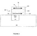
- FIG 3 shows an MRAM cell 200 and processor element 340 according to an embodiment of the invention.
- the MRAM cell 200 as shown in Figure 3 is formed over a substrate 350.
- the substrate 350 can include a corresponding processor element 340.
- the structure shown in Figure 3 is desirable because the MRAM cell 200 does not include any transistor elements. Therefore, the MRAM cell can be formed during the conductor processing of an integrated circuit. That is, semiconductors within the substrate 350 typically include conductive lines formed over the substrate 350.
- the MRAM cell provides the advantage of being formed during the formation of the conductive lines. This provides ease of producing, and allows the MRAM cell 200 to be formed proximate to the corresponding processor element 340.
- an array of MRAM cells can be formed over an array of processor elements. Physically, each MRAM cell can be formed over the corresponding processor element. This provides a space efficient implementation of the memory array and the parallel processor.
- FIG 4 shows an MRAM cell 200, processor element 340 and DRAM cell 460 according to an embodiment of the invention.
- the MRAM cell 200 as shown in Figure 3 is formed over a substrate 350 and the DRAM cell 460.
- the MRAM/DRAM memory cells structure of Figure 4 allows both the DRAM cell 460 and the MRAM cell 200 to be written to and read from at the same time.
- a single word line WL can be connected to both the MRAM cell 200 and the DRAM cell 460.
- the shared MRAM/DRAM memory cells provide for the integration of MRAM and DRAM memory cells on a common substrate.
- the integrated memory cell allows for the formation of integrated memory cell arrays in which large amounts of data can be easily transferred from MRAM cells to DRAM cells, and/or from DRAM cells to MRAM cells.
- FIG. 5 shows a circuit schematic of an integrated MRAM cell and DRAM cell according to an embodiment of the invention.
- This embodiment includes a shared DRAM/MRAM memory cell 500 that includes a first memory cell 510, and a non-volatile memory cell 520 that is interfaced to the first memory cell 510.
- the first memory cell 510 can include a DRAM memory cell.
- the DRAM memory cell shown in Figure 5 includes a DRAM controlling transistor QD and a storage capacitor CD. Charge is both stored on the storage capacitor CD, and sensed from the storage capacitor CD through a word line WL and a bit line DBL.
- the non-volatile memory cell 520 can include an MRAM memory cell.
- the MRAM memory cell shown in Figure 5 includes an MRAM controlling transistor QM and a magnetoresistive tunnel junction (MTJ) memory cell.
- Magnetic states of the MRAM memory cell 520 are set by magnetic fields generated by current flowing through bit line MBL and write word line MWL.
- the magnetic state of the MRAM cell 520 is sensed, by sensing a resistance of the MTJ memory cell through a sense line MSL and a bit line MBL.
- the magnetic orientation of the MTJ memory cell determines the resistance across the MTJ memory cell.
- Figure 6 shows a shared MRAM/DRAM memory cell according to an embodiment of the invention.
- Figure 6 is an embodiment of a physical implementation of the MRAM/DRAM memory cells of Figure 4 and Figure 5.
- This embodiment can be fabricated on a substrate 600 of silicon. Diffusion regions in the substrate 600 can be used to form the drain (D) and source (S) of the MRAM controlling transistor QM and the DRAM controlling transistor QD.
- a trench formed in the substrate 600 can be filled with conductive material and dielectric material to form the DRAM capacitor CD.
- a first metallization layer can be used to form conductive contacts to the source (S) of the MRAM controlling transistor, the gate (G) of the MRAM controlling transistor, the drain (D) of the DRAM controlling transistor, the gate (G) of the DRAM controlling transistor and the DRAM capacitor.
- the source of the MRAM controlling transistor can be connected to ground (GND).
- the gate (G) of the MRAM controlling transistor can be connected to the word line (WL).
- the drain (D) of the DRAM controlling transistor can be connected to the DRAM bit line DBL.
- the source (S) of the DRAM controlling transistor is connected to a first terminal of the DRAM capacitor CD. This connection can be formed by forming the source (S) of the DRAM controlling transistor so close to the first terminal of the DRAM capacitor CD that source (S) and the first terminal are electrically connected.
- a second terminal of the DRAM capacitor CD can be connected to ground (GND).
- a second metallization layer can be used to form a conductive contact to the magnetic tunnel junction (MTJ) memory cell of the MRAM memory cell.
- the conductive contact can be connected to the MRAM bit line MBL.
- a third metallization layer can also be used to form a conductive contact to the magnetic tunnel junction device of the MRAM memory cell.
- the conductive contact can be connected to the MRAM sense line MSL.
- a fourth metallization layer can be used to form the MRAM write word line MWL.
- the metallization layers can be formed from Tantalum, Copper or Aluminum.
- Figure 7 shows multiple MRAM cells 711 - 714, multiple processor elements 721 - 724, and a master processor 760 according to another embodiment of the invention. As shown in Figure 7, the multiple processor elements 721 - 724 are connected to the master processor 760.
- the master processor 760 can receive processed data from each of the processor elements. The master processor 760 can then combine the processed data from each of the processor elements, and provide additional processing of the combined data if required.
- Figure 8 shows an array of image sensors 801 - 804, multiple MRAM cells 811-814, multiple DRAM cells 831 - 834, multiple processor elements 821 - 824, and a master processor 860 according to another embodiment of the invention.
- the image sensors 801 - 804 can include amorphous silicon diodes, thin film photo sensors, and active pixel sensors.
- the image sensors can be fabricated over the MRAM cells.
- the image sensors are electrically connected to the MRAM cells.
- Each image sensor receives an image, and generates a voltage that is proportional to the intensity of the received image.
- a local processor element creates a digital representation of the generated voltage is stored in a corresponding MRAM cell.
- Each of the processor elements 821 - 824 can perform image processing of the image received by the image sensors 801 - 804. The processing can be performed in parallel, and then summed at the master processor 860.
- the DRAM cells 831 - 834 can be used to optimize processing.
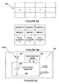
- FIGS 8A, 8B and 8C shows an array of image sensors, DRAM cells and processor elements in greater detail.
- Figure 8A shows a top-view of an array of neighboring sensor pixels X, Y, Z within an array of sensor pixels 850.
- Figure 8B shows a cross-section of neighboring sensors pixels X, Y and Z, corresponding MRAM cells X, Y and Z and corresponding local processing elements X, Y and Z.
- the sensor pixels can be a thin film sensor array.
- the MRAM cells can be a part of an MRAM array.
- the sensor pixels can receive light as indicated in Figure 8C.
- Figure 8C shows a block diagram of an individual sensor pixel including the sensor (which can include a light sensitive diode 891 and a sense capacitor 892), a local processing element 893 and a non-volatile MRAM cell 894.
- the local processing element 893 and the non-volatile MRAM cell can include a two-way interface.
- the local processing element 893 can include an interface to a master processor that includes data (DOUT) and controls (CONTROL).
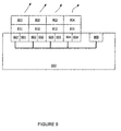
- Figure 9 shows an array of light emitters 901 - 904, multiple MRAM cells 911-914, multiple DRAM cells 931 - 934, multiple processor elements 921 - 924, and a master processor 960 according to another embodiment of the invention.
- the MRAM cells can be used to store a value that adjustably sets the intensity of light emitted from each of the light emitters.
- the processor elements 921 - 924 can perform image processing in parallel providing more efficient processing than a non-parallel processing system.
- FIG 10 shows a circuit schematic of an MRAM and a light emitter according to an embodiment of the invention.
- This embodiment includes a light emitting diode (LED) 1010 that emits light.
- the amount of light emitted from the LED 1010 can be dependent upon a bias current flowing through the LED 1010.
- the intensity of the light emitted by the LED 1010 can be controlled by a resistance of a magnetic tunnel junction 1020.
- the resistance of the tunnel magnetic junction 1020 is dependent upon the state of the tunnel magnetic junction 1020. Therefore, the states of the magnetic tunnel junction 1020 control the intensity of the light emitted from the LED 1010.
- the states of the tunnel magnetic junction 1020 are determined by the application of a magnetic field Happ.
- the embodiment shown in Figure 10 further includes a bias transistor 1030 and a bias controller 1040.
- the bias controller 1040 can be configured so that the bias current flowing through the LED 1010 is dependent upon the resistance of the tunnel magnetic junction 1020, and therefore, the state of the tunnel magnetic junction 1020.
- the embodiment of Figure 10 is merely an example of circuit in which the intensity of a light source is modulated based upon the state of a magnetic tunnel junction. Many other possible circuits that provide for modulation of a light source depending upon the resistance of a magnetic tunnel junction are possible.
- An alternate embodiment includes the light emitting source being a laser diode such as a vertical cavity surface emitting laser (VCSEL).
- VCSEL vertical cavity surface emitting laser
- the invention can also use other modulated light sources.
- Figure 11 shows a substrate including an MRAM structure and light emitter according to an embodiment of the invention.
- the substrate includes a controlling transistor 1120, a magnetic tunnel junction 1130 and a controllable light emitting device 1140.
- the controlling transistor 1120, the magnetic tunnel junction 1130 and the controllable light emitting device 1140 can be electrically connected through conductive lines 1152, 1154, 1156.
- the controlling transistor 1120 can be formed in the substrate 1110, and include a source 1112, a drain 1114 and a poly-Si gate 1116.
- the magnetic tunnel junction 1130 can be formed over the controlling transistor 1120.
- the controlling transistor 1120 can be electrically connected to a light emitting device 1140.
- Standard semiconductor processing steps can be used to form the controlling transistor 1120.
- the light emitting device 1140 can include a PIN diode that includes a p-contact 1142, a p-GaAs layer 1143, a p-AlGaAs layer 1144, an i-GaAs layer 1145 an n-AlGaAs layer 1446 and an n-contact 1147.
- Standard semiconductor processing steps can be used to form the light emitting device 1140.
- Standard semiconductor processing steps can be used to form the conductive lines 1152, 1154, 1156. Similar semiconductor processing steps can be used to form the conductive layers of the MTJ 1130.
- the embodiment of Figure 11 provides an integrated MTJ 1130 and light emitting device 1140 that can provide selective comb filtering. As previously described, the filtering is dependent upon the materials and physical characteristics of the MTJ 1130.
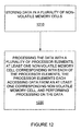
- Figure 12 is a flow chart that includes acts according to an embodiment of the invention. The acts provide a method of parallel processing.
- a first act 1210 includes storing data in a plurality of non-volatile memory cells.
- a second act 1220 includes processing the data with a plurality of processor elements, at least one non-volatile memory cell corresponding with each of the processor elements, the processor elements each accessing data from an at least one corresponding non-volatile memory cell, and performing processing on the data.
Landscapes
- Engineering & Computer Science (AREA)
- Theoretical Computer Science (AREA)
- Physics & Mathematics (AREA)
- Computer Hardware Design (AREA)
- Chemical & Material Sciences (AREA)
- Nanotechnology (AREA)
- General Engineering & Computer Science (AREA)
- General Physics & Mathematics (AREA)
- Computing Systems (AREA)
- Mathematical Physics (AREA)
- Crystallography & Structural Chemistry (AREA)
- Hall/Mr Elements (AREA)
- Mram Or Spin Memory Techniques (AREA)
- Semiconductor Memories (AREA)
- Microcomputers (AREA)
Abstract
A parallel processor includes a plurality of non-volatile memory cells
(110,112,114,116), and a plurality of processor elements (120,122,124,126). At least
one non-volatile memory cell (110,112,114,116) corresponds with each of the
processor elements (120,122,124,126). The processor elements (120,122,124,126)
each access data from at least one corresponding non-volatile memory cell
(110,112,114,116). The processor elements (120,122,124,126) perform processing on
the data. The non-volatile memory cells (110,112,114,116) can include magnetic
memory cells.
Description
- The invention relates generally to electronic memory. More particularly, the invention relates to a non-volatile memory parallel processor.
- Computer systems are becoming increasingly sophisticated allowing users to perform a continually increasing variety of computing tasks at faster rates. As a result, complex computations are required to be performed by the computer systems at greater rates.
- Parallel processing is a method in which multiple operations or computations are performed in parallel. That is, instead of performing the operations serially, the operations are performed simultaneously. The results of the simultaneous operations can be combined after being individually completed. The net result is that total computations can be performed at greater speeds.
- Parallel processing can be particularly useful for applications that receive or generate a large number of inputs or outputs, and provide processing of the inputs and outputs. For example, the reception or generation of images can benefit from parallel processing. Image processing can include operations being performed on many image elements (for example, pixels).
- Presently, parallel processing computing systems are typically volatile. That is, generally the parallel processing computing systems fail if power to the computing systems is turned off. In some applications, this reduces the efficiency of the computing system. It can be advantageous to be able to maintain the parallel processing data during a power shut down, so that the processing can be easily restarted.
- The present invention seeks to provide an improved parallel processor.
- According to an aspect of the present invention there is provided a parallel processor as specified in
claim 1. - The preferred embodiment provides apparatus and a method of parallel processing that is non-volatile, that is adaptable for image processing and/or which is easily integratable.
- Thus, the invention includes an apparatus and method for parallel processing. The apparatus and method are adaptable for image processing. Additionally, the parallel processing apparatus can be efficiently integrated.
- An embodiment of the invention includes a parallel processor. The parallel processor includes a plurality of non-volatile memory cells. The parallel processor additionally includes a plurality of processor elements. At least one non-volatile memory cell corresponds with each of the processor elements. The processor elements each access data from at least one corresponding non-volatile memory cell. The processor elements perform processing on the data. The non-volatile memory cells can include magnetic memory.
- Embodiments of the present invention are described below, by way of example only, with reference to the drawings, in which:
- Figure 1 shows an embodiment of processing.
- Figure 2 shows a magnetic memory cell according to an embodiment of the invention.
- Figure 3 shows an MRAM cell and processor element according to an embodiment of the invention.
- Figure 4 shows an MRAM cell, processor element and DRAM cell according to an embodiment of the invention.
- Figure 5 shows a circuit schematic of an integrated MRAM cell and DRAM cell according to an embodiment of the invention.
- Figure 6 shows a structure of an integrated MRAM cell and DRAM cell according to an embodiment of the invention.
- Figure 7 shows multiple MRAM cells, multiple processor elements, multiple DRAM cells, and a master processor according to another embodiment of the invention.
- Figure 8 shows an array of image sensors, multiple MRAM cells, multiple DRAM cells, multiple processor elements, and a master processor according to another embodiment of the invention.
- Figures 8A, 8B and 8C shows an array of image sensors, DRAM cells and processor elements in greater detail.
- Figure 9 shows an array of light emitters, multiple MRAM cells, multiple DRAM cells, multiple processor elements, and a master processor according to another embodiment of the invention.
- Figure 10 shows a circuit schematic of an MRAM and a light emitter according to an embodiment of the invention.
- Figure 11 shows a substrate including an MRAM structure and light emitter according to an embodiment of the invention.
- Figure 12 is a flow chart that includes acts according to an embodiment of the invention.
-
- As shown in the drawings for purposes of illustration, the described embodiments provide apparatus for and a method of parallel processing data stored in MRAM elements with multiple processor elements. The parallel processing apparatus can be efficiently integrated.
- Figure 1 shows an embodiment of the invention. More specifically, the embodiment of Figure 1 includes a parallel processor. The parallel processor includes a plurality of
non-volatile memory cells processor elements non-volatile memory cell processor elements processor elements non-volatile memory cell processor elements non-volatile memory cell - Control and
data lines processor elements non-volatile memory cells non-volatile memory cell - The data stored in the
non-volatile memory cell - As will be described, the
non-volatile memory cells processor elements non-volatile memory cells magnetic memory cell corresponding processor - As will be described, an embodiment includes each non-volatile memory cell being interfaced with a corresponding at least one dynamic random access memory (DRAM) cell. This embodiment can provide performance advantages because non-volatile memory and DRAM each provide performance advantages. By combining the two types of memory, the advantages provides by each can be utilized.
- The embodiment of Figure 1 includes a
master processor 130. The master processor can combine processed data from each of theprocessor elements processor elements master processor 130, but rather, includes at least one of theprocessor elements processor elements - Figure 2 shows a magnetic memory cell (MRAM) 200 according to an embodiment of the invention. The
MRAM memory cell 200 includes asense layer 220, adielectric region 230 and areference layer 210. The orientation of magnetization within thesense layer 220 is non-fixed, and can assume two stable orientations as shown by the arrow M1. The reference layer 210 (also referred to as a pinned magnetic region) has a fixed magnetic orientation as depicted by the arrow M2. Thedielectric region 230 generally provides electrical insulation between thesense layer 220 and thereference layer 210. - As previously stated, the orientation of magnetization of the
sense layer 220 can assume two stable orientations. These two orientations, which are either parallel or anti-parallel to the magnetic orientation of thereference layer 210, determine the logical state of theMRAM memory cell 200. - The magnetic orientation of the
MRAM memory cell 200 is set (written to) by controlling electrical currents flowing through the word lines and the bit lines, and therefore, by the corresponding magnetic fields induced by the electrical currents. Because the word line and the bit line operate in combination to switch the orientation of magnetization of the selected memory cell (that is, to write to the memory cell), the word line and the bit line can be collectively referred to as write lines. Additionally, the write lines can also be used to read the logic value stored in the memory cells. - The orientation of magnetization of the
sense layer 220 is determined in response to electrical currents applied to the bit lines (BL) and the word lines (WL) during a write operation to the MRAM memory cell. The electrical currents applied to the bit line and the word line set the orientation of the magnetization of the sense layer depending upon the directions of the currents flowing through the bit line and the word line, and therefore, the directions of the induced magnetic fields created by the currents flowing through the bit line and the word line. - The
MRAM memory cell 200 is read by sensing a resistance across the MRAM memory cells. The resistance is sensed through the word lines and the bit lines. - The
reference layer 210 and thesense layer 220 can be made of a ferromagnetic material. - If the magnetization of the
sense layer 220 and thereference layer 210 of the MTJ memory cell are in the same direction, the orientation of the MTJ memory cell can be referred to as being "parallel." If the magnetization of thesense layer 220 and thereference layer 210 of the MTJ memory cell are in opposite directions, the orientation of the MTJ memory cell can be referred to as being "anti-parallel." The two orientations, parallel and anti-parallel, can correspond to MTJ memory cell states of low or high resistance respectively. - The
dielectric regions 230 allow quantum mechanical tunneling to occur between thereference layer 210 and thesense layer 220. The tunneling is electron spin dependent, causing the resistance of the MTJ memory cell to be a function of the relative orientations of the magnetization directions of thereference layer 210 and thesense layer 220. The resistance state of the MJT memory cell can be sensed to determine the magnetization orientations of thereference layer 210 and thesense layer 220. - The resistance of the MTJ memory cell is a first value (R) if the magnetization orientation of the MTJ memory cell is parallel and a second value (R+delta) if the magnetization orientation is anti-parallel. The invention, however, is not limited to the magnetization orientation of the two layers, or to just two layers.
- The
dielectric region 230 can be made of aluminum oxide, silicon dioxide, tantalum oxide, silicon nitride, aluminum nitride, or magnesium oxide. However, other dielectrics and certain semiconductor materials may also be used for thedielectric region 230. The thickness of thedielectric region 230 may range from about 0.5 nanometers to about three nanometers. However, the invention is not limited to this range. - The
sense layer 220 may be made of a ferromagnetic material. Thereference layer 210 can be implemented as a synthetic ferrimagnet (SF), also referred to as an artificial antiferromagnet. - The non-volatile memory cell can include other types of memory including ferroelectric FeRAM and Flash memory. These other non-volatile types of memory are well known in the art of digital electronics.
- Figure 3 shows an
MRAM cell 200 andprocessor element 340 according to an embodiment of the invention. TheMRAM cell 200 as shown in Figure 3 is formed over asubstrate 350. Thesubstrate 350 can include acorresponding processor element 340. - As will be described, the structure shown in Figure 3 is desirable because the
MRAM cell 200 does not include any transistor elements. Therefore, the MRAM cell can be formed during the conductor processing of an integrated circuit. That is, semiconductors within thesubstrate 350 typically include conductive lines formed over thesubstrate 350. The MRAM cell provides the advantage of being formed during the formation of the conductive lines. This provides ease of producing, and allows theMRAM cell 200 to be formed proximate to the correspondingprocessor element 340. - Structurally, an array of MRAM cells can be formed over an array of processor elements. Physically, each MRAM cell can be formed over the corresponding processor element. This provides a space efficient implementation of the memory array and the parallel processor.
- Figure 4 shows an
MRAM cell 200,processor element 340 andDRAM cell 460 according to an embodiment of the invention. TheMRAM cell 200 as shown in Figure 3 is formed over asubstrate 350 and theDRAM cell 460. - The MRAM/DRAM memory cells structure of Figure 4 allows both the
DRAM cell 460 and theMRAM cell 200 to be written to and read from at the same time. A single word line WL can be connected to both theMRAM cell 200 and theDRAM cell 460. - The shared MRAM/DRAM memory cells provide for the integration of MRAM and DRAM memory cells on a common substrate. As will be shown later, the integrated memory cell allows for the formation of integrated memory cell arrays in which large amounts of data can be easily transferred from MRAM cells to DRAM cells, and/or from DRAM cells to MRAM cells.
- Figure 5 shows a circuit schematic of an integrated MRAM cell and DRAM cell according to an embodiment of the invention. This embodiment includes a shared DRAM/
MRAM memory cell 500 that includes afirst memory cell 510, and anon-volatile memory cell 520 that is interfaced to thefirst memory cell 510. - The
first memory cell 510 can include a DRAM memory cell. The DRAM memory cell shown in Figure 5 includes a DRAM controlling transistor QD and a storage capacitor CD. Charge is both stored on the storage capacitor CD, and sensed from the storage capacitor CD through a word line WL and a bit line DBL. - The
non-volatile memory cell 520 can include an MRAM memory cell. The MRAM memory cell shown in Figure 5 includes an MRAM controlling transistor QM and a magnetoresistive tunnel junction (MTJ) memory cell. Magnetic states of theMRAM memory cell 520 are set by magnetic fields generated by current flowing through bit line MBL and write word line MWL. The magnetic state of theMRAM cell 520 is sensed, by sensing a resistance of the MTJ memory cell through a sense line MSL and a bit line MBL. As previously described, the magnetic orientation of the MTJ memory cell determines the resistance across the MTJ memory cell. - Figure 6 shows a shared MRAM/DRAM memory cell according to an embodiment of the invention. Figure 6 is an embodiment of a physical implementation of the MRAM/DRAM memory cells of Figure 4 and Figure 5.
- This embodiment can be fabricated on a
substrate 600 of silicon. Diffusion regions in thesubstrate 600 can be used to form the drain (D) and source (S) of the MRAM controlling transistor QM and the DRAM controlling transistor QD. - A trench formed in the
substrate 600 can be filled with conductive material and dielectric material to form the DRAM capacitor CD. - A first metallization layer can be used to form conductive contacts to the source (S) of the MRAM controlling transistor, the gate (G) of the MRAM controlling transistor, the drain (D) of the DRAM controlling transistor, the gate (G) of the DRAM controlling transistor and the DRAM capacitor. The source of the MRAM controlling transistor can be connected to ground (GND). The gate (G) of the MRAM controlling transistor can be connected to the word line (WL). The drain (D) of the DRAM controlling transistor can be connected to the DRAM bit line DBL. The source (S) of the DRAM controlling transistor is connected to a first terminal of the DRAM capacitor CD. This connection can be formed by forming the source (S) of the DRAM controlling transistor so close to the first terminal of the DRAM capacitor CD that source (S) and the first terminal are electrically connected. A second terminal of the DRAM capacitor CD can be connected to ground (GND).
- A second metallization layer can be used to form a conductive contact to the magnetic tunnel junction (MTJ) memory cell of the MRAM memory cell. The conductive contact can be connected to the MRAM bit line MBL.
- A third metallization layer can also be used to form a conductive contact to the magnetic tunnel junction device of the MRAM memory cell. The conductive contact can be connected to the MRAM sense line MSL.
- A fourth metallization layer can be used to form the MRAM write word line MWL.
- The metallization layers can be formed from Tantalum, Copper or Aluminum.
- Figure 7 shows multiple MRAM cells 711 - 714, multiple processor elements 721 - 724, and a
master processor 760 according to another embodiment of the invention. As shown in Figure 7, the multiple processor elements 721 - 724 are connected to themaster processor 760. - The
master processor 760 can receive processed data from each of the processor elements. Themaster processor 760 can then combine the processed data from each of the processor elements, and provide additional processing of the combined data if required. - Figure 8 shows an array of image sensors 801 - 804, multiple MRAM cells 811-814, multiple DRAM cells 831 - 834, multiple processor elements 821 - 824, and a
master processor 860 according to another embodiment of the invention. - The image sensors 801 - 804 can include amorphous silicon diodes, thin film photo sensors, and active pixel sensors. The image sensors can be fabricated over the MRAM cells. The image sensors are electrically connected to the MRAM cells.
- Each image sensor receives an image, and generates a voltage that is proportional to the intensity of the received image. A local processor element creates a digital representation of the generated voltage is stored in a corresponding MRAM cell.
- Each of the processor elements 821 - 824 can perform image processing of the image received by the image sensors 801 - 804. The processing can be performed in parallel, and then summed at the
master processor 860. The DRAM cells 831 - 834 can be used to optimize processing. - Figures 8A, 8B and 8C shows an array of image sensors, DRAM cells and processor elements in greater detail.
- Figure 8A shows a top-view of an array of neighboring sensor pixels X, Y, Z within an array of
sensor pixels 850. - Figure 8B shows a cross-section of neighboring sensors pixels X, Y and Z, corresponding MRAM cells X, Y and Z and corresponding local processing elements X, Y and Z. The sensor pixels can be a thin film sensor array. The MRAM cells can be a part of an MRAM array. The sensor pixels can receive light as indicated in Figure 8C.
- Figure 8C shows a block diagram of an individual sensor pixel including the sensor (which can include a light
sensitive diode 891 and a sense capacitor 892), alocal processing element 893 and anon-volatile MRAM cell 894. Thelocal processing element 893 and the non-volatile MRAM cell can include a two-way interface. Thelocal processing element 893 can include an interface to a master processor that includes data (DOUT) and controls (CONTROL). - Figure 9 shows an array of light emitters 901 - 904, multiple MRAM cells 911-914, multiple DRAM cells 931 - 934, multiple processor elements 921 - 924, and a
master processor 960 according to another embodiment of the invention. - As will be described, the MRAM cells can be used to store a value that adjustably sets the intensity of light emitted from each of the light emitters.
- As previously described, the processor elements 921 - 924 can perform image processing in parallel providing more efficient processing than a non-parallel processing system.
- Figure 10 shows a circuit schematic of an MRAM and a light emitter according to an embodiment of the invention. This embodiment includes a light emitting diode (LED) 1010 that emits light. The amount of light emitted from the
LED 1010 can be dependent upon a bias current flowing through theLED 1010. - The intensity of the light emitted by the
LED 1010 can be controlled by a resistance of amagnetic tunnel junction 1020. As previously described, the resistance of the tunnelmagnetic junction 1020 is dependent upon the state of the tunnelmagnetic junction 1020. Therefore, the states of themagnetic tunnel junction 1020 control the intensity of the light emitted from theLED 1010. The states of the tunnelmagnetic junction 1020 are determined by the application of a magnetic field Happ. - The embodiment shown in Figure 10 further includes a
bias transistor 1030 and abias controller 1040. Thebias controller 1040 can be configured so that the bias current flowing through theLED 1010 is dependent upon the resistance of the tunnelmagnetic junction 1020, and therefore, the state of the tunnelmagnetic junction 1020. - The embodiment of Figure 10 is merely an example of circuit in which the intensity of a light source is modulated based upon the state of a magnetic tunnel junction. Many other possible circuits that provide for modulation of a light source depending upon the resistance of a magnetic tunnel junction are possible.
- An alternate embodiment includes the light emitting source being a laser diode such as a vertical cavity surface emitting laser (VCSEL). The invention can also use other modulated light sources.
- Figure 11 shows a substrate including an MRAM structure and light emitter according to an embodiment of the invention. The substrate includes a controlling
transistor 1120, amagnetic tunnel junction 1130 and a controllablelight emitting device 1140. - The controlling
transistor 1120, themagnetic tunnel junction 1130 and the controllablelight emitting device 1140 can be electrically connected throughconductive lines - The controlling
transistor 1120 can be formed in thesubstrate 1110, and include asource 1112, adrain 1114 and a poly-Si gate 1116. Themagnetic tunnel junction 1130 can be formed over the controllingtransistor 1120. The controllingtransistor 1120 can be electrically connected to alight emitting device 1140. - Standard semiconductor processing steps can be used to form the controlling
transistor 1120. - The
light emitting device 1140 can include a PIN diode that includes a p-contact 1142, a p-GaAs layer 1143, a p-AlGaAs layer 1144, an i-GaAs layer 1145 an n-AlGaAs layer 1446 and an n-contact 1147. - Standard semiconductor processing steps can be used to form the
light emitting device 1140. - Standard semiconductor processing steps can be used to form the
conductive lines MTJ 1130. - The embodiment of Figure 11 provides an
integrated MTJ 1130 and light emittingdevice 1140 that can provide selective comb filtering. As previously described, the filtering is dependent upon the materials and physical characteristics of theMTJ 1130. - Figure 12 is a flow chart that includes acts according to an embodiment of the invention. The acts provide a method of parallel processing.
- A
first act 1210 includes storing data in a plurality of non-volatile memory cells. - A
second act 1220 includes processing the data with a plurality of processor elements, at least one non-volatile memory cell corresponding with each of the processor elements, the processor elements each accessing data from an at least one corresponding non-volatile memory cell, and performing processing on the data. - The disclosures in United States patent application No10/625,016, from which this application claims priority, and in the abstract accompanying this application are incorporated herein by reference.
Claims (10)
- A parallel processor including:a plurality of non-volatile memory cells (110,112,114,116);a plurality of processor elements (120,122,124,126), at least one non-volatile memory cell (110,112,114,116) corresponding with each of the processor elements (120,122,124,126), the processor elements (120,122,124,126) each accessing data from an at least one corresponding non-volatile memory cell (110,112,114,116), and performing processing on the data.
- A parallel processor as in claim 1, wherein the non-volatile memory cells (110,112,114,116) comprise magnetic memory cells (200).
- A parallel processor as in claim 1 or 2, wherein each processor element (120,122,124,126) can access a plurality of non-volatile memory cells (110,112,114,116).
- A parallel processor as in claim 2 or 3, wherein each non-volatile memory cell (110,112,114,116) is interfaced with a corresponding at least one dynamic random access memory (DRAM) cell (460).
- A parallel processor as in claim 2, 3 or 4, wherein each magnetic memory cell (200) is formed adjacent to a substrate (350), and the corresponding processor element (340) is formed in the substrate (350) adjacent to the magnetic memory cell (200).
- A parallel processor as in claim 2, 3 or 4, wherein each magnetic memory cell (200) is formed adjacent to a substrate (350), and the corresponding processor element (340) and DRAM cell (460) are formed in the substrate (350) adjacent to the magnetic memory cell (200).
- A parallel processor as in any preceding claim, including:a master processor (760) for receiving processed data from the plurality of processor element (721,722,723,724).
- A parallel processor as in claim 7, wherein the master processor (760) is operable to perform additional processing of the data.
- A parallel processor as in any preceding claim, including:an array of image sensors, an image sensor corresponding with each of the magnetic memory cells (110, 112,114,116).
- A parallel processor as in claim 9, wherein each image sensor is operable to receive image data that can be stored in a corresponding non-volatile memory element.
Applications Claiming Priority (2)
| Application Number | Priority Date | Filing Date | Title |
|---|---|---|---|
| US10/625,016 US7079148B2 (en) | 2003-07-23 | 2003-07-23 | Non-volatile memory parallel processor |
| US625016 | 2003-07-23 |
Publications (1)
| Publication Number | Publication Date |
|---|---|
| EP1501020A1 true EP1501020A1 (en) | 2005-01-26 |
Family
ID=33490876
Family Applications (1)
| Application Number | Title | Priority Date | Filing Date |
|---|---|---|---|
| EP04253575A Withdrawn EP1501020A1 (en) | 2003-07-23 | 2004-06-15 | A non-volatile memory parallel processor |
Country Status (5)
| Country | Link |
|---|---|
| US (1) | US7079148B2 (en) |
| EP (1) | EP1501020A1 (en) |
| JP (1) | JP2005050337A (en) |
| CN (1) | CN1577312A (en) |
| TW (1) | TWI263165B (en) |
Families Citing this family (15)
| Publication number | Priority date | Publication date | Assignee | Title |
|---|---|---|---|---|
| GB0207307D0 (en) * | 2002-03-27 | 2002-05-08 | Koninkl Philips Electronics Nv | In-pixel memory for display devices |
| US7412028B2 (en) * | 2004-01-20 | 2008-08-12 | Ge Medical Systems, Israel Ltd. | Methods and system for multi-modality imaging |
| US20060078178A1 (en) * | 2004-09-18 | 2006-04-13 | Will Shatford | Swipe sensor |
| WO2006074176A2 (en) * | 2005-01-05 | 2006-07-13 | The Regents Of The University Of California | Memory architectures including non-volatile memory devices |
| US7568115B2 (en) * | 2005-09-28 | 2009-07-28 | Intel Corporation | Power delivery and power management of many-core processors |
| JP4989899B2 (en) * | 2006-01-27 | 2012-08-01 | ルネサスエレクトロニクス株式会社 | Semiconductor processing unit |
| JP4989900B2 (en) * | 2006-01-31 | 2012-08-01 | ルネサスエレクトロニクス株式会社 | Parallel processing unit |
| US7447846B2 (en) * | 2006-04-12 | 2008-11-04 | Mediatek Inc. | Non-volatile memory sharing apparatus for multiple processors and method thereof |
| US8131912B2 (en) | 2007-09-27 | 2012-03-06 | Kabushiki Kaisha Toshiba | Memory system |
| US8731891B2 (en) * | 2011-07-28 | 2014-05-20 | Saudi Arabian Oil Company | Cluster 3D petrophysical uncertainty modeling |
| KR20130116705A (en) | 2012-04-16 | 2013-10-24 | 삼성전자주식회사 | Mram : magnetic random access memory device and method for addressing threrof |
| US9058126B2 (en) * | 2012-09-10 | 2015-06-16 | Texas Instruments Incorporated | Nonvolatile logic array with retention flip flops to reduce switching power during wakeup |
| KR20160101901A (en) | 2013-12-24 | 2016-08-26 | 인텔 코포레이션 | Hybrid memory and mtj based mram bit-cell and array |
| KR102393342B1 (en) * | 2017-10-26 | 2022-05-03 | 삼성전자주식회사 | Semiconductor memory and method |
| US11114146B2 (en) * | 2019-11-25 | 2021-09-07 | International Business Machines Corporation | Nanosecond non-destructively erasable magnetoresistive random-access memory |
Citations (1)
| Publication number | Priority date | Publication date | Assignee | Title |
|---|---|---|---|---|
| WO2003023913A1 (en) * | 2001-09-06 | 2003-03-20 | Brown University Research Fondation | Magneto-optoelectronic switch and sensor |
Family Cites Families (11)
| Publication number | Priority date | Publication date | Assignee | Title |
|---|---|---|---|---|
| GB9424598D0 (en) * | 1994-12-06 | 1995-01-25 | Philips Electronics Uk Ltd | Semiconductor memory with non-volatile memory transistor |
| US5754484A (en) * | 1996-05-13 | 1998-05-19 | Motorola Inc. | Apparatus and method for utilization of limited write memory |
| US7506020B2 (en) * | 1996-11-29 | 2009-03-17 | Frampton E Ellis | Global network computers |
| US6611241B1 (en) * | 1997-12-02 | 2003-08-26 | Sarnoff Corporation | Modular display system |
| US6552745B1 (en) | 1998-04-08 | 2003-04-22 | Agilent Technologies, Inc. | CMOS active pixel with memory for imaging sensors |
| US6297989B1 (en) * | 1999-02-26 | 2001-10-02 | Micron Technology, Inc. | Applications for non-volatile memory cells |
| DE10015193A1 (en) * | 2000-03-27 | 2001-10-25 | Infineon Technologies Ag | Highly integrated system-on-chip systems with non-volatile memory units |
| US7051326B2 (en) * | 2000-12-13 | 2006-05-23 | International Business Machines Corporation | Code image distribution in a multi-node network of processors |
| JP3838086B2 (en) * | 2001-12-12 | 2006-10-25 | ソニー株式会社 | Image processing apparatus and method |
| US7027836B2 (en) * | 2002-09-10 | 2006-04-11 | Eastman Kodak Company | Method and system for establishing a communication network |
| US6713810B1 (en) * | 2003-02-10 | 2004-03-30 | Micron Technology, Inc. | Non-volatile devices, and electronic systems comprising non-volatile devices |
-
2003
- 2003-07-23 US US10/625,016 patent/US7079148B2/en not_active Expired - Fee Related
-
2004
- 2004-03-11 TW TW093106502A patent/TWI263165B/en not_active IP Right Cessation
- 2004-05-24 CN CNA2004100457475A patent/CN1577312A/en active Pending
- 2004-06-15 EP EP04253575A patent/EP1501020A1/en not_active Withdrawn
- 2004-07-23 JP JP2004215103A patent/JP2005050337A/en active Pending
Patent Citations (1)
| Publication number | Priority date | Publication date | Assignee | Title |
|---|---|---|---|---|
| WO2003023913A1 (en) * | 2001-09-06 | 2003-03-20 | Brown University Research Fondation | Magneto-optoelectronic switch and sensor |
Non-Patent Citations (4)
| Title |
|---|
| AIZAWA K ET AL: "On sensor image compression for high pixel rate imaging: pixel parallel and column parallel architectures", PROCEEDINGS OF THE INTERNATIONAL CONFERENCE ON IMAGE PROCESSING (ICIP) LAUSANNE, SEPT. 16 - 19, 1996, NEW YORK, IEEE, US, vol. VOL. 1, 16 September 1996 (1996-09-16), pages 1019 - 1022, XP010202832, ISBN: 0-7803-3259-8 * |
| JAEHYUK HUH ET AL: "Exploring the design space of future CMPs", DEPARTMENT OF COMPUTER SCIENCE, 8 September 2001 (2001-09-08), THE UNIVERSITY OF TEXAS AT AUSTIN, pages 199 - 210, XP010558960 * |
| R. DESIKAN, C. R. LEFURGY, S. W. KECKLER, D. BURGER: "Tech Report TR-02-47: On-chip MRAM as a High-Bandwidth, Low-Latency Replacement for DRAM Physical Memories", DEPARTMENT OF COMPUTER SCIENCES, 27 September 2002 (2002-09-27), THE UNIVERSITY OF TEXAS AT AUSTIN, XP002303537, Retrieved from the Internet <URL:http://www.cs.utexas.edu/ftp/pub/techreports/tr02-47.pdf> [retrieved on 20041102] * |
| SIKORA A: "DIE ZUKUNFT DES SPEICHERS FERAM, MRAM UND ANDERE SPEICHERTECHNOLOGIEN AUF DER SUCHE NACH DEM HEILIGEN GRAL - TEIL 2", ELEKTRONIK, FRANZIS VERLAG GMBH. MUNCHEN, DE, vol. 51, no. 6, 19 March 2002 (2002-03-19), pages 52 - 57, XP001162640, ISSN: 0013-5658 * |
Also Published As
| Publication number | Publication date |
|---|---|
| TWI263165B (en) | 2006-10-01 |
| JP2005050337A (en) | 2005-02-24 |
| US20050017979A1 (en) | 2005-01-27 |
| US7079148B2 (en) | 2006-07-18 |
| TW200506713A (en) | 2005-02-16 |
| CN1577312A (en) | 2005-02-09 |
Similar Documents
| Publication | Publication Date | Title |
|---|---|---|
| JP4700259B2 (en) | Memory element array having a pair of magnetic bits sharing a common conductor | |
| US6894918B2 (en) | Shared volatile and non-volatile memory | |
| US6473337B1 (en) | Memory device having memory cells with magnetic tunnel junction and tunnel junction in series | |
| KR101148395B1 (en) | Memory cell and method of forming a magnetic tunnel junction mtj of a memory cell | |
| US6657270B2 (en) | Magnetic random access memory using bipolar junction transistor, and method for fabricating the same | |
| US6946712B2 (en) | Magnetic memory device using SOI substrate | |
| US7079148B2 (en) | Non-volatile memory parallel processor | |
| KR102426892B1 (en) | Memory device with tunable probabilistic state | |
| WO2018236361A1 (en) | FERROELECTRIC FIELD EFFECT TRANSISTORS (FEFET) HAVING INTERFACE LAYER DESIGNED AS A BAND | |
| US6798689B2 (en) | Integrated memory with a configuration of non-volatile memory cells and method for fabricating and for operating the integrated memory | |
| US20020084500A1 (en) | Magnetic random access memory and method for manufacturing the same | |
| KR20200050368A (en) | Read circuit for magnetic tunnel junction (mtj) memory | |
| JP2024528302A (en) | Spin-orbit torque magnetoresistive random access memory array | |
| US20140016390A1 (en) | Logical memory architecture, in particular for mram, pcram, or rram | |
| CN108028060A (en) | Autoregistration memory array | |
| US20210327487A1 (en) | Sensing scheme for stt-mram using low-barrier nanomagnets | |
| US20220051709A1 (en) | Row-wise tracking of reference generation for memory devices | |
| KR100422945B1 (en) | A method for writing of a magnetic random access memory using bipolar junction transistor | |
| WO2005043541A2 (en) | Method and system for providing a programmable current source for a magnetic memory | |
| US11004898B2 (en) | Method for manufacturing a magnetic tunnel junction device and device manufactured using such method | |
| KR100604752B1 (en) | Manufacturing method of magnetic ram | |
| WO2024024497A1 (en) | Storage device, electronic apparatus, and method for controlling storage device | |
| HK1064508A (en) | Shared volatile and non-volatile memory |
Legal Events
| Date | Code | Title | Description |
|---|---|---|---|
| PUAI | Public reference made under article 153(3) epc to a published international application that has entered the european phase |
Free format text: ORIGINAL CODE: 0009012 |
|
| AK | Designated contracting states |
Kind code of ref document: A1 Designated state(s): AT BE BG CH CY CZ DE DK EE ES FI FR GB GR HU IE IT LI LU MC NL PL PT RO SE SI SK TR |
|
| AX | Request for extension of the european patent |
Extension state: AL HR LT LV MK |
|
| 17P | Request for examination filed |
Effective date: 20050415 |
|
| 17Q | First examination report despatched |
Effective date: 20050610 |
|
| AKX | Designation fees paid |
Designated state(s): DE |
|
| STAA | Information on the status of an ep patent application or granted ep patent |
Free format text: STATUS: THE APPLICATION IS DEEMED TO BE WITHDRAWN |
|
| 18D | Application deemed to be withdrawn |
Effective date: 20051021 |