EP1500975A2 - Procédé pour la fabrication de microstructures optiques - Google Patents
Procédé pour la fabrication de microstructures optiques Download PDFInfo
- Publication number
- EP1500975A2 EP1500975A2 EP04016312A EP04016312A EP1500975A2 EP 1500975 A2 EP1500975 A2 EP 1500975A2 EP 04016312 A EP04016312 A EP 04016312A EP 04016312 A EP04016312 A EP 04016312A EP 1500975 A2 EP1500975 A2 EP 1500975A2
- Authority
- EP
- European Patent Office
- Prior art keywords
- surface topography
- etching
- effective surface
- optically effective
- smoothed
- Prior art date
- Legal status (The legal status is an assumption and is not a legal conclusion. Google has not performed a legal analysis and makes no representation as to the accuracy of the status listed.)
- Withdrawn
Links
Images
Classifications
-
- G—PHYSICS
- G02—OPTICS
- G02B—OPTICAL ELEMENTS, SYSTEMS OR APPARATUS
- G02B3/00—Simple or compound lenses
- G02B3/0006—Arrays
- G02B3/0012—Arrays characterised by the manufacturing method
- G02B3/0025—Machining, e.g. grinding, polishing, diamond turning, manufacturing of mould parts
-
- G—PHYSICS
- G02—OPTICS
- G02B—OPTICAL ELEMENTS, SYSTEMS OR APPARATUS
- G02B3/00—Simple or compound lenses
- G02B3/0006—Arrays
- G02B3/0012—Arrays characterised by the manufacturing method
-
- G—PHYSICS
- G03—PHOTOGRAPHY; CINEMATOGRAPHY; ANALOGOUS TECHNIQUES USING WAVES OTHER THAN OPTICAL WAVES; ELECTROGRAPHY; HOLOGRAPHY
- G03F—PHOTOMECHANICAL PRODUCTION OF TEXTURED OR PATTERNED SURFACES, e.g. FOR PRINTING, FOR PROCESSING OF SEMICONDUCTOR DEVICES; MATERIALS THEREFOR; ORIGINALS THEREFOR; APPARATUS SPECIALLY ADAPTED THEREFOR
- G03F7/00—Photomechanical, e.g. photolithographic, production of textured or patterned surfaces, e.g. printing surfaces; Materials therefor, e.g. comprising photoresists; Apparatus specially adapted therefor
- G03F7/0005—Production of optical devices or components in so far as characterised by the lithographic processes or materials used therefor
Definitions
- the invention relates to a process for producing optically effective microstructures in at least one step an optically effective surface topography on a Substrate is produced by a mechanical process and in at least one further finishing step the Surface topography is smoothed.
- the invention relates to the production of lenses, lens arrays and prismatic structures with a high aspect ratio, large structural heights and with a cross-sectional area smaller than 1.5 mm 2 .
- a typical example of the invention Method produced microstructure is a plano-convex Aspherical cylindrical lens, which acts as a collimator of the fast axis used in high-power diode lasers.
- the high must be divergent laser beam are focused as much as possible (See R. Diehl, High Power Diode Lasers, Fundamentals, Technology, Applications, 78 / Topics in Applied Physics).
- the Cylinder lens extremely accurate and with low Tolerances are manufactured. Typical dimensions of such Cylindrical lenses are at a width of 1 mm, one Arrow height (optically effective structure height) of 0.3 mm at a total height of 0.8 mm and a length of 12 mm.
- the cylindrical lenses for high-power diode lasers consist of brittle-hard materials, such as optical glasses or quartz glass.
- the brittle character of the materials and the large structural height of the cylindrical lens usually make a multi-step manufacturing process required.
- the machining processes are divided regularly in the processing steps pre-grinding, fine grinding and Polishing (see Volker R. Sinhoff, Feinbearbeitung optical Glasses in no - series, WZL - Reports from the Production Technology, Volume 6/97, Shaker Verlag).
- Grinding as a mechanical removal process is the optical effective surface topography generated while polishing as a finishing step to an improvement of Surface quality while maintaining the Shape accuracy aims.
- thermally induced smoothing means Electron radiation described. The method is based on a targeted melting of the surface. Heal through it near-surface defects (cracks). Decisive disadvantage This finishing step is the change of Surface topography. Due to the viscous state of the material during smoothing the material tries the take energetically favorable state of a ball. This distorts the during mechanical Pre-processing achieved dimension of optically effective Structure.
- Refractive microlenses for ultra-flat photolithographic projection systems is a Production method for microlenses described in which a layer (about 1 micron to 50 microns thick) photoresist on applied to a substrate polished on both sides of quartz glass becomes. Then the paint is passed through a mask develops and thereby an arrangement of cylinders Photoresist produced on the substrate.
- the cylinders off Photoresist are prepared by plasma assisted etching, namely transferred reactive ion etching in the quartz glass. The Atoms from the photoresist surface and the quartz glass are removed by the ions at the same time, until the lens completely etched into the substrate.
- the lens may be slightly changed after the ion etching. These form changes are tried to prevent, in which the Etch rate is changed during the etching.
- One Finishing step is not in this method necessary, since the surface condition of the two-sided polished substrate by the reactive ion etching nearly not changed.
- This manufacturing method has compared to the mechanical described above Manufacturing process has the advantage that with high Precision economically large quantities optically more effective Structures can be produced.
- the disadvantage is the low etching rate and the limitation of using this method achievable structure height to a maximum of 0.1 mm. aspheric Cylindrical lenses acting as a collimator of the fast-axis in High-power diode lasers are used, can be therefore do not make with this method.
- the task is to specify a method that the industrial production of optically active Microstructures, in particular structured arrays with high Precision and tight tolerances allowed. With the procedure In particular, structural heights of more than 0.1 mm can be manufactured industrially.
- This object is achieved in a method of initially mentioned type solved in that the optical effective surface topography photolithographically masked and by etching, in particular by plasma-assisted Dry etching is smoothed.
- Dry etching in particular plasma etching or reactive ion etching in Consideration.
- a first step is by a mechanical method, in particular imaging grinding, Ultraschallschwingläppen or Laserabtragen the optical producing effective surface topography on the substrate; in at least one further finishing step, the resulting from the mechanical abrasion process Surface defects by etching, in particular by smoothed plasma-assisted dry etching.
- Dry etching processes are in particular the plasma etching or reactive ion etching into consideration.
- the plasma etching and the reactive ion etching is found to be advantageous. Both methods are based on a mixed physical / chemical Etching mechanism.
- plasma etching are the etching-active particles reactive radicals, weak ion-assisted.
- reactive ion etching the etching-active particles reactive radicals, strongly ion-assisted with reactive ions.
- the inventive method is especially for substrates suitable, characterized by plasma-assisted etching can be processed, such as quartz and silicon.
- substrates suitable, characterized by plasma-assisted etching can be processed, such as quartz and silicon.
- the method can be in particular cylindrical lenses for Produce high-power diode laser, due to the Radiation characteristic of the diodes of a high numerical Aperture need to collimate the light.
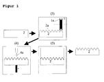
- a grinding tool 1 is produced, the Grinding surface 1a as a negative mold one on a substrate.
- To produce the grinding tool 1 come Processes that are used in metallic Materials Contours with shape accuracies smaller than 1 ⁇ m let generate. This dimensional accuracy is required so that the lens array to be produced in the required Tolerance is. Suitable is, for example, the Microfiber erosion or a combination of Diamond turning and electroplating of the Grinding tool 1.
- the negative mold 1a of the Tool 1 by grinding (3) in several rows on a Substrate 2 transferred from quartz glass.
- the usage of Abrasive surfaces 1a with fine-grained abrasive media For example, a diamond grain with a middle Grain of 7 microns, ensures low damage during the preparation of the optically active Surface topography 2a.
- the first step smoothed surface topography 2 a, in which she initially photolithographically masked (4) and then is smoothed by reactive ion etching (5).
- the masking involves the application of the radiation-sensitive photoresist 4a in the spin-coating process (4) on the substrate 2. Subsequently, the Photoresist varnish 4a in a furnace, not shown at baked at a temperature of about 150 ° - 200 ° C. Possibly. the photoresist is exposed. A local exposure of the photoresist and a subsequent Development step can be to adapt or optimize the Profile shape of the microstructure are used.
- the applied photoresist is also used as a mask designated.
- the masking is followed by reactive ion etching (RIBE) (5) to the optically effective surface topography to smooth, without changing the contour.
- RIBE reactive ion etching
- Ion beam etching becomes the substrate during reactive ion etching 2 processed over the entire surface, so that during the reactive Ion etching (5) the entire optically effective Surface topography (2 a) is irradiated simultaneously.
- the atoms of the photoresist layer and the underlying substrate are formed by ion etching ablated and any defects in the surface topography of the substrate smoothed.
- the surface topography 2 a can be a star-shaped structure (i.e. Structures extend radially from the center to the edge of the Substrate).
- Structures extend radially from the center to the edge of the Substrate.
Landscapes
- Physics & Mathematics (AREA)
- Engineering & Computer Science (AREA)
- Manufacturing & Machinery (AREA)
- General Physics & Mathematics (AREA)
- Optics & Photonics (AREA)
- Semiconductor Lasers (AREA)
- Surface Treatment Of Glass (AREA)
Applications Claiming Priority (4)
| Application Number | Priority Date | Filing Date | Title |
|---|---|---|---|
| DE10333230 | 2003-07-21 | ||
| DE10333230 | 2003-07-21 | ||
| DE10354181 | 2003-11-19 | ||
| DE10354181A DE10354181A1 (de) | 2003-07-21 | 2003-11-19 | Verfahren zur Herstellung von optischen Mikrostrukturen |
Publications (2)
| Publication Number | Publication Date |
|---|---|
| EP1500975A2 true EP1500975A2 (fr) | 2005-01-26 |
| EP1500975A3 EP1500975A3 (fr) | 2006-01-18 |
Family
ID=33491671
Family Applications (1)
| Application Number | Title | Priority Date | Filing Date |
|---|---|---|---|
| EP04016312A Withdrawn EP1500975A3 (fr) | 2003-07-21 | 2004-07-12 | Procédé pour la fabrication de microstructures optiques |
Country Status (1)
| Country | Link |
|---|---|
| EP (1) | EP1500975A3 (fr) |
Cited By (3)
| Publication number | Priority date | Publication date | Assignee | Title |
|---|---|---|---|---|
| CN103722182A (zh) * | 2013-12-12 | 2014-04-16 | 郑丽萍 | 一种锗透镜车削的方法 |
| CN109946922A (zh) * | 2019-04-23 | 2019-06-28 | 马颖鏖 | 光学表面微轮廓二维直接成像制造及光学表面平整修形方法 |
| CN115421229A (zh) * | 2022-09-19 | 2022-12-02 | 上海交通大学 | 一种su-8微透镜阵列的光刻-抛光直接成型制造方法 |
Family Cites Families (6)
| Publication number | Priority date | Publication date | Assignee | Title |
|---|---|---|---|---|
| CA2071598C (fr) * | 1991-06-21 | 1999-01-19 | Akira Eda | Dispositif optique et methode de fabrication connexe |
| DE4234740C2 (de) * | 1992-10-15 | 1997-12-11 | Joachim Hentze | Verfahren zur Herstellung von optischen Elementen |
| NO941307L (no) * | 1993-04-12 | 1994-10-13 | Hughes Aircraft Co | Fremgangsmåte ved fremstilling av mikro-optiske elementer |
| US6271900B1 (en) * | 1998-03-31 | 2001-08-07 | Intel Corporation | Integrated microlens and color filter structure |
| JP2002361597A (ja) * | 2001-06-11 | 2002-12-18 | Nikon Corp | マイクロレンズアレイの製造方法、マイクロレンズアレイ、光学系、投影露光装置 |
| FR2827270B1 (fr) * | 2001-07-13 | 2004-01-02 | Centre Nat Rech Scient | Procede de fabrication de pieces microscopiques |
-
2004
- 2004-07-12 EP EP04016312A patent/EP1500975A3/fr not_active Withdrawn
Cited By (3)
| Publication number | Priority date | Publication date | Assignee | Title |
|---|---|---|---|---|
| CN103722182A (zh) * | 2013-12-12 | 2014-04-16 | 郑丽萍 | 一种锗透镜车削的方法 |
| CN109946922A (zh) * | 2019-04-23 | 2019-06-28 | 马颖鏖 | 光学表面微轮廓二维直接成像制造及光学表面平整修形方法 |
| CN115421229A (zh) * | 2022-09-19 | 2022-12-02 | 上海交通大学 | 一种su-8微透镜阵列的光刻-抛光直接成型制造方法 |
Also Published As
| Publication number | Publication date |
|---|---|
| EP1500975A3 (fr) | 2006-01-18 |
Similar Documents
| Publication | Publication Date | Title |
|---|---|---|
| EP4166271B1 (fr) | Procédé de fabrication d'au moins une couche d'un solide pleine courbée ou partiellement courbée par sections | |
| DE2614951C3 (de) | Verfahren zur Herstellung einer Flüssigkristall-Zelle | |
| DE10318681B4 (de) | Verfahren und Vorrichtung zum Entfernen eines Randbereichs einer Substratschicht und zur Substratbeschichtung sowie Substrat | |
| WO2020182934A1 (fr) | Procédé et dispositif pour placer un matériau sur un support | |
| DE102021214310A1 (de) | Verfahren und Vorrichtung zum Erzeugen mindestens einer Hohlstruktur, EUVSpiegel und EUV-Lithographiesystem | |
| DE102021210093A1 (de) | Optisches Element mit Kühlkanälen und optische Anordnung | |
| EP1647535A1 (fr) | Procédé pour microstructurer substrats de verre plat | |
| DE102015204478B4 (de) | Verfahren zum Glätten einer Oberfläche und optisches Element | |
| EP0847329B1 (fr) | Procede de production de couches polymeres structurees en trois dimensions pour l'optique integre | |
| EP1500975A2 (fr) | Procédé pour la fabrication de microstructures optiques | |
| DE102008054882A1 (de) | Reparaturverfahren für optische Elemente mit Beschichtung und entsprechende optische Elemente | |
| DE102017202649A1 (de) | Verfahren zum Bearbeiten eines Werkstücks bei der Herstellung eines optischen Elements | |
| DE10354181A1 (de) | Verfahren zur Herstellung von optischen Mikrostrukturen | |
| DE102018105958B4 (de) | Verfahren zur Herstellung eines Werkzeugs für die Herstellung mikrostrukturier-ter optischer Bauteile und Werkzeug für die Herstellung mikrostrukturierter op-tischer Bauteile | |
| WO2005098082A2 (fr) | Dispositif de revetement bilateral de substrats au moyen d'une couche hydrophobe | |
| DE102011003077A1 (de) | Verfahren zur Herstellung eines Substrates für ein reflektives optisches Element für die EUV-Lithographie | |
| WO2022184482A1 (fr) | Procédé de fabrication d'un corps principal d'un élément optique, corps principal d'un élément optique et système d'exposition par projection | |
| EP3517654B1 (fr) | Procédé de fabrication d'un insert de moule à (sous-)microstructures ainsi que pièce à usiner à (sous-)microstructures | |
| DE102009021330A1 (de) | Verfahren zum Verringern der Oberflächenrauhigkeit einer porösen Oberfläche | |
| DE102024110083B4 (de) | Verfahren und Vorrichtung zur Formkorrektur eines optischen Bauelements mittels Laserstrahlung | |
| DE19844025A1 (de) | Reaktives Ionen(strahl)ätzen von Oberflächen | |
| EP1412967A1 (fr) | Procede de fabrication d'une lentille | |
| DE102019202222A1 (de) | Ablenkspiegel aus Diamant sowie Verfahren zur Herstellung | |
| AT411755B (de) | Vorrichtung und verfahren zum modifizieren einer werkstück-oberfläche mit hilfe von photonen-strahlung | |
| DE102009019122A1 (de) | Verfahren zur Herstellung einer Projektionsbelichtungsanlage für die Mikrolithographie |
Legal Events
| Date | Code | Title | Description |
|---|---|---|---|
| PUAI | Public reference made under article 153(3) epc to a published international application that has entered the european phase |
Free format text: ORIGINAL CODE: 0009012 |
|
| AK | Designated contracting states |
Kind code of ref document: A2 Designated state(s): AT BE BG CH CY CZ DE DK EE ES FI FR GB GR HU IE IT LI LU MC NL PL PT RO SE SI SK TR |
|
| AX | Request for extension of the european patent |
Extension state: AL HR LT LV MK |
|
| PUAL | Search report despatched |
Free format text: ORIGINAL CODE: 0009013 |
|
| AK | Designated contracting states |
Kind code of ref document: A3 Designated state(s): AT BE BG CH CY CZ DE DK EE ES FI FR GB GR HU IE IT LI LU MC NL PL PT RO SE SI SK TR |
|
| AX | Request for extension of the european patent |
Extension state: AL HR LT LV MK |
|
| RIC1 | Information provided on ipc code assigned before grant |
Ipc: G03F 7/00 20060101ALI20051125BHEP Ipc: G02B 3/00 20060101AFI20051125BHEP |
|
| AKX | Designation fees paid | ||
| STAA | Information on the status of an ep patent application or granted ep patent |
Free format text: STATUS: THE APPLICATION IS DEEMED TO BE WITHDRAWN |
|
| 18D | Application deemed to be withdrawn |
Effective date: 20060729 |
|
| REG | Reference to a national code |
Ref country code: DE Ref legal event code: 8566 |