EP1500943B1 - Commutateur de sélection pour un canal à grande vitesse - Google Patents
Commutateur de sélection pour un canal à grande vitesse Download PDFInfo
- Publication number
- EP1500943B1 EP1500943B1 EP20040008248 EP04008248A EP1500943B1 EP 1500943 B1 EP1500943 B1 EP 1500943B1 EP 20040008248 EP20040008248 EP 20040008248 EP 04008248 A EP04008248 A EP 04008248A EP 1500943 B1 EP1500943 B1 EP 1500943B1
- Authority
- EP
- European Patent Office
- Prior art keywords
- high speed
- unit
- channel selector
- speed channel
- selector switch
- Prior art date
- Legal status (The legal status is an assumption and is not a legal conclusion. Google has not performed a legal analysis and makes no representation as to the accuracy of the status listed.)
- Expired - Lifetime
Links
- 238000011156 evaluation Methods 0.000 claims description 36
- 238000012360 testing method Methods 0.000 claims description 20
- 239000000758 substrate Substances 0.000 claims description 10
- 239000000463 material Substances 0.000 claims description 4
- 230000005693 optoelectronics Effects 0.000 description 25
- 238000005259 measurement Methods 0.000 description 8
- 238000004891 communication Methods 0.000 description 4
- 230000008878 coupling Effects 0.000 description 3
- 238000010168 coupling process Methods 0.000 description 3
- 238000005859 coupling reaction Methods 0.000 description 3
- 230000003287 optical effect Effects 0.000 description 3
- PNEYBMLMFCGWSK-UHFFFAOYSA-N aluminium oxide Inorganic materials [O-2].[O-2].[O-2].[Al+3].[Al+3] PNEYBMLMFCGWSK-UHFFFAOYSA-N 0.000 description 2
- 230000005540 biological transmission Effects 0.000 description 2
- 238000012854 evaluation process Methods 0.000 description 2
- 238000000034 method Methods 0.000 description 2
- 230000003071 parasitic effect Effects 0.000 description 2
- 239000004810 polytetrafluoroethylene Substances 0.000 description 2
- 229920001343 polytetrafluoroethylene Polymers 0.000 description 2
- 230000015556 catabolic process Effects 0.000 description 1
- 239000002131 composite material Substances 0.000 description 1
- 238000006731 degradation reaction Methods 0.000 description 1
- 238000011990 functional testing Methods 0.000 description 1
- 239000002241 glass-ceramic Substances 0.000 description 1
- 230000010354 integration Effects 0.000 description 1
- 239000000523 sample Substances 0.000 description 1
- 239000004065 semiconductor Substances 0.000 description 1
- 230000008054 signal transmission Effects 0.000 description 1
Images


Classifications
-
- H—ELECTRICITY
- H04—ELECTRIC COMMUNICATION TECHNIQUE
- H04B—TRANSMISSION
- H04B17/00—Monitoring; Testing
- H04B17/0082—Monitoring; Testing using service channels; using auxiliary channels
-
- G—PHYSICS
- G01—MEASURING; TESTING
- G01R—MEASURING ELECTRIC VARIABLES; MEASURING MAGNETIC VARIABLES
- G01R31/00—Arrangements for testing electric properties; Arrangements for locating electric faults; Arrangements for electrical testing characterised by what is being tested not provided for elsewhere
- G01R31/28—Testing of electronic circuits, e.g. by signal tracer
- G01R31/317—Testing of digital circuits
- G01R31/3181—Functional testing
- G01R31/319—Tester hardware, i.e. output processing circuits
- G01R31/31903—Tester hardware, i.e. output processing circuits tester configuration
- G01R31/31905—Interface with the device under test [DUT], e.g. arrangements between the test head and the DUT, mechanical aspects, fixture
-
- G—PHYSICS
- G01—MEASURING; TESTING
- G01R—MEASURING ELECTRIC VARIABLES; MEASURING MAGNETIC VARIABLES
- G01R31/00—Arrangements for testing electric properties; Arrangements for locating electric faults; Arrangements for electrical testing characterised by what is being tested not provided for elsewhere
- G01R31/28—Testing of electronic circuits, e.g. by signal tracer
- G01R31/317—Testing of digital circuits
- G01R31/3181—Functional testing
- G01R31/319—Tester hardware, i.e. output processing circuits
- G01R31/31903—Tester hardware, i.e. output processing circuits tester configuration
- G01R31/31912—Tester/user interface
Definitions
- Embodiments of the invention are related to the field of high speed communications. More specifically, embodiments of the invention are directed to test equipment for high speed communication systems.
- JP 04 068549 A describes a semiconductor test equipment for switching from a DC test circuit to a functional test circuit or vice versa by providing the equipment with a base ring to hold a probe and a rotatable ring which is installed between a socket of a DUT and each test circuit and is rotated as the need arises.
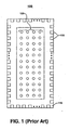
- FIG. 1 shows a top view of an exemplary prior art optoelectronic module 100 fabricated within an integrated circuit (IC) 110.
- the module 100 has an array of vertical cavity surface emitting lasers (VCSELs) 120 and a large number of high speed pads 130 disposed around the periphery of the IC 110. For clarity, not all of the high speed pads 130 are shown. Other pads such as supply pads and ground pads (not shown) are also typically disposed around the periphery of the IC 110.
- VCSELs vertical cavity surface emitting lasers
- VCSELs are replaced by photodetectors.
- an additional optical subassembly that includes coupling and focusing optics and optical mulitplexers or demultiplexers reside on top of the VCSELs or photodetectors.
- FIG. 2 illustrates an exemplary prior art evaluation board 200 used to test massively parallel optoelectronic modules.
- module 100 is placed on the evaluation board 200 and the individual high speed pads (e.g., high speed pads 130 of FIG. 1 ) are coupled via data lines 210 to a plurality of connectors 220.
- the connectors 220 are coupled via data cables 230 to either an evaluation tool such as a signal tester) or to a termination impedance 250.
- the present invention provides a high speed channel selector switch according to claim 1.
- a high speed channel selector switch that selectively couples one of a plurality of data lines of a device under test to a signal line in accordance with the invention is disclosed.
- the remaining data lines of the device under test are concurrently coupled to respective termination impedances disposed within the switch. This facilitates evaluating high speed communication devices, such as massively parallel optoelectronic systems by reducing the necessity for manually connecting the data lines individually to an evaluation tool and for terminating the remaining data lines.
- Embodiments in accordance with the invention provide a switch for selectively coupling a signal line with a selected one of a plurality of data lines of an evaluation board.
- the switch enables a user to select one of the data lines for testing while simultaneously terminating the remaining data lines. This facilitates rapidly connecting and disconnecting leads when testing/evaluating high speed communication devices such as massively parallel optoelectronic systems. Additionally, the amount of wear exhibited in the operation of conventional evaluation boards is reduced. Further, embodiments in accordance with the invention reduce the likelihood of erroneously connecting or terminating leads that is possible when done manually.
- FIG. 3 illustrates a high speed channel selector switch 300 in accordance with embodiments in accordance with the invention.
- switch 300 comprises a fixed unit 400, that is coupled with a plurality of high speed data lines 310.
- the high speed data lines convey signals to the high speed pads of a massively parallel optoelectronic module that is being tested.
- High speed channel selector switch 300 further comprises a rotatable unit 500, that is disposed above fixed unit 400. Rotatable unit 500 is used to selectively couple one of the high speed data lines 310 to the signal line 320.
- Rotatable unit 500 also comprises a plurality of contacts that couple the remaining high speed data lines to respective termination impedances.
- the termination impedances are disposed within rotatable unit 500 itself.
- high speed channel selector switch 300 further comprises a knob 600 that facilitates turning rotatable unit 500.
- knob 600 has index marks on its top surface or some other markings to assist a user in determining which of the high speed data lines 310 is selectively coupled with signal line 320.
- FIG.s 4A and 4B are top and side sectional views respectively of electrical paths in a fixed unit 400 of a high speed channel selector switch (e.g., high speed channel selector switch 300 of FIG. 3 ) in accordance with embodiments of the invention.
- fixed unit 400 is coupled with an evaluation board.
- fixed unit 400 can also be embedded within an evaluation board.
- fixed unit 400 comprises 24 outer high speed pads typically shown as 410a, 410b, and 410c disposed in a circular pattern upon a substrate 420. While the embodiment of FIG. 4A shows the outer high speed pads disposed in a circular pattern, embodiments in accordance with the invention are well suited to have the high speed pads disposed in a different manner. Similarly, while substrate 420 is shown in FIG. 4A to be configured as a circular structure, embodiments in accordance with the invention are well suited to substrate structures having other shapes as well.
- each of the 24 outer high speed pads is electrically coupled to a respective high speed data line typically shown as 310a, 310b, and 310c via a respective signal input/output line typically shown as 411a, 411b, and 411c.
- contact 412a couples outer high speed pad 410a to signal input/output line 411a.
- substrate 420 is a disk shaped circuit board made of a microwave substrate material such as Alumina. While embodiments in accordance with the invention discussed specifically recite Alumina, other materials, such as glass ceramics, various PTFE composites and non-PTFE laminates, etc can be used for substrate 420.
- fixed unit 400 further comprises an additional high speed pad (e.g., signal pad 415) that is disposed proximate to the center of substrate 420.
- Signal pad 415 is electrically coupled to a signal line (e.g., signal line 320 of FIG. 3 ) via a signal input/output line 416.
- FIG. 4B is a side sectional view of fixed unit 400 taken through signal input/output line 416, signal pad 415, outer high speed pad 410a, and signal input/output line 411a.
- signal pad 415 is electrically coupled with signal line 320 via contact 414 and with signal input/output line 416.
- high speed pad 410a is coupled with high speed data line 3 10a through via 412a and signal input/output line 411a.
- contacts which electrically couple the top ground region 421 with bottom ground region 423.
- top ground region 421 appears to be multiple sections in the side perspective of FIG. 4B , in one embodiment in accordance with the invention, the top ground region 421 is one continuous region.
- conductive balls are attached to signal pad 415, each of the outer high speed pads 410, and the top ground region 421 in order to provide an electrically conductive path between the fixed unit 400 and the rotatable unit 500.
- FIG.s 5A and 5B are bottom and side sectional views respectively of rotatable unit 500 of a high speed channel selector switch in accordance with the invention.
- the bottom surface of rotatable unit 500 comprises 24 outer high speed pads typically shown as 510a, 510b, and 510c disposed in a circular pattern near the outer edge of rotatable unit 500.
- FIG. 5A shows the outer high speed pads 510 disposed in a circular pattern
- embodiments in accordance with the invention are well suited to have the high speed pads disposed in a different manner.
- Rotatable unit 500 further comprises a central high speed pad 520 that is disposed proximate to the center of rotatable unit 500. Referring now to FIG.
- the outer high speed pads 410 of the fixed unit 400 are configured in a matching pattern with reference to the outer high speed pads 510 of rotatable unit 500.
- each of the outer high speed pads 410 is aligned with and electrically coupled to a corresponding outer high speed pad 510.
- an electrical signal can be conveyed between each of the outer high speed pads 410a, 410b, 410c, etc., to a corresponding outer high speed pad 510a, 510b, 510c, etc.
- the use of the high-speed channel selector switch enables implementation of a more compact and robust evaluation platform. Due to fewer measurement errors and less mechanical wear of the evaluation equipment, the accuracy of measurement is enhanced.
- central high speed pad 520 is aligned with signal pad 415 of FIG. 4A .
- one of the outer high speed pads 510a, 510b, 510c (e.g., outer high speed pad 510a) is electrically coupled with central high speed pad 520 via signal line 511 and contact 512a.
- Central high speed pad 520 is coupled with signal line 511 via contact 521.
- the width, thickness, and material comprising signal line 511 are selected to control the impedance characteristics of signal line 511.
- the termination impedance could be a low parasitic surface-mount or flip-chip component mounted on the rotatable unit.
- the termination impedance can also reside on the fixed unit or external to the switch, in which case routing lines should be established from the pads of the rotatable unit to the pads of the termination impedances. Additionally, the remaining outer high speed pads of rotatable unit 500 (i.e., those pads not electrically coupled to central high speed pad 520) are electrically coupled with respective termination impedances typically shown as 530 via a respective terminating line 531 typically shown as 53b, 53c, etc. In an embodiment in accordance with the invention, the termination impedances 530 are embedded within rotatable unit 500 and have low parasitics.
- a user can selectively couple a high speed data line 310 with signal line 320 using rotatable unit 500 in conjunction with fixed unit 400.
- a user can turn rotatable unit 500 until an electrical path is formed between outer high speed pad 410a and signal pad 415 via outer high speed pad 510a, signal line 511, and central high speed pad 520.
- the remaining high speed data lines 310 are coupled with a termination impedance 530.
- the user can select outer high speed pad 410b by turning rotatable unit 500 counterclockwise relative to fixed unit 400 (e.g., using knob 600 of FIG.
- signal line 511 now couples outer high speed pad 410b and signal pad 415, and outer high speed pad 410a is now coupled with a termination impedance 530.
- FIG. 6 is a side section view of an electrical path conducted by a fixed unit 400 and a rotatable unit 500 of a high speed channel selector switch (e.g., high speed channel selector switch 300 of FIG. 3 ) in accordance with one embodiment of the invention. It is appreciated that FIG. 6 shows the side section views of fixed unit 400 and rotatable unit 500 ( FIG.s 4B and 5B respectively).
- an electrical signal is being sent from an evaluation device (not shown) to an optical channel of an optoelectronic module (not shown). In another implementation, a signal is being sent from an optoelectronic module to the evaluation device.
- an electrical signal from an evaluation device is conveyed from signal line 320 to signal pad 415 via contact 414 and is then conveyed to central high speed pad 520. From central high speed pad 520, the electrical signal is passed to signal line 511 and high speed pad 510 via contact 521. From there the electrical signal is conveyed to data line 310a through high speed pad 410a, contact 412a, and signal input/output line 411a.
- an evaluation device e.g., a signal generator
- a plurality of signals may be simultaneously conveyed from an optoelectronic module to fixed unit 400 via a plurality of data lines (e.g., data lines 310 of FIG. 3 ). However, only one of these signals is electrically coupled to signal line 320 via rotatable unit 500. The remaining electrical signals are coupled with respective termination impedances (e.g., termination impedance 530 of Figure 5A ) via remaining high speed pads 510 and the terminating transmission lines 531 (e.g. high speed pad 510b and terminating transmission line 531b). A user can select which of the plurality of signals is coupled to signal line 320 by turning knob 600 as described above.
- termination impedances e.g., termination impedance 530 of Figure 5A
- FIG. 7 is a top view of an evaluation board 700 for testing a massively parallel optoelectronic module in accordance with embodiments of the invention.
- a plurality of high speed channel selector switches typically shown as 300a, 300b, 300c, and 300d are coupled with a plurality of high speed data lines 710.
- the electrical paths shown in FIG.s 4A and 4B reside in fixed units of the high speed channel selector switches 300a-300d.
- the high speed channel selector switches 300a-300d are coupled with a substrate 750 of evaluation board 700.
- the electrical paths shown in FIG.s 4A and 4B may, in accordance with embodiments of the invention, be fabricated within the substrate of evaluation board 700.
- optoelectronic module 100 is electrically coupled with the high speed data lines 710.
- optoelectronic module 100 is a massively parallel high speed optoelectronic system.
- optoelectronic module 100 is a receiver and has 96 high speed pads (e.g., high speed pads 130 of FIG. 1 ) that serve as electrical signal outputs from a receiver integrated circuit that amplifies and/or processes the analog signals from a photodetector array.
- the optoelectronic module 100 is a transmitter, in which case the high speed pads serve as electrical signal inputs of a transmitter integrated circuit which drives a VCSEL array.
- Each of the high speed pads of the optoelectronic module 100 is coupled to one of the high speed channel selector switches 300a-300d through an individual high speed data line 710.
- the electrical coupling between the high speed pads of optoelectronic device 100 and the high speed data lines 710 is formed in any convenient fashion. In one embodiment of the invention, individual wire bonds are formed between the high speed pads of the optoelectronic module 100 and the high speed data lines 710.
- each high speed channel selector switch 300a-300d has a signal pad (e.g., signal pad 415 of FIG.s 4A and 4B ).
- the signal pads electrically couple to connectors 720a-720d via respective signal lines (e.g., signal line 320 of Figure 3 ).
- the signal pads also electrically couple to one of the high speed data lines 710 via signal input/output data lines, high speed pads, and signal lines as described above.
- a cable 730a, 730b, 730c, or 730d electrically couples one of the high speed channel selector switches 300a-300d with a respective evaluation device 740.
- Embodiments in accordance with the invention add a level of integration in the evaluation of massively parallel systems.
- the invention facilitates quickly switching between channels when testing massively parallel high speed optoelectronic modules. Additionally, the remaining channels are concurrently coupled with a termination impedance. As a result, significant savings in time to perform a measurement is achieved.
- embodiments in accordance with the invention eliminate the need to manually connect and/or terminate individual cables in evaluation board 700, less physical degradation of the connectors (e.g., connectors 720a-720d of FIG. 7 ) occurs. As a result, fewer measurement errors and less mechanical wear of the evaluation equipment occurs and the accuracy of measurement is enhanced.
- the use of the high-speed channel selector switch also enables implementation of a more compact and robust evaluation platform.
Landscapes
- Physics & Mathematics (AREA)
- Electromagnetism (AREA)
- Engineering & Computer Science (AREA)
- Computer Networks & Wireless Communication (AREA)
- Signal Processing (AREA)
- Tests Of Electronic Circuits (AREA)
- Keying Circuit Devices (AREA)
- Rotary Switch, Piano Key Switch, And Lever Switch (AREA)
Claims (13)
- Commutateur sélecteur (300) de canal à grande vitesse comprenant :une première unité (400) comportant une pluralité de contacts (410) adaptée pour se coupler électriquement à une pluralité de lignes (310) de données à grande vitesse d'un dispositif sous test, ladite première unité (400) comportant en outre un contact (415) de signal adapté pour se coupler électriquement à une ligne (320) de signal ; etune deuxième unité (500) adaptée pour coupler électriquement de façon sélective un de ladite pluralité de contacts (410) au dit contact (415) de signal et coupler en outre électriquement ceux restants de ladite pluralité de contacts (410) à une pluralité d'impédances (530) de terminaison respectives, de sorte qu'une de ladite pluralité de lignes (310) de données à grande vitesse soit couplée à ladite ligne (320) de signal et celles restantes de la pluralité de lignes (310) de données à grande vitesse soient couplées à ladite pluralité d'impédances (530) de terminaison respectives, la deuxième unité (500) étant rotative par rapport à la première unité (400).
- Sélecteur (300) de canal à grande vitesse selon la revendication 1, dans lequel ladite pluralité de contacts (410) est configurée dans un cercle.
- Sélecteur (300) de canal à grande vitesse selon la revendication 2, dans lequel ledit contact (415) de signal est situé au centre dudit cercle.
- Sélecteur (300) de canal à grande vitesse selon l'une des revendications précédentes, dans lequel ladite première unité (400) est exploitable pour être fixée à une carte (700) d'évaluation.
- Commutateur sélecteur (300) de canal à grande vitesse selon l'une des revendications précédentes, dans lequel ladite pluralité d'impédances de terminaison respectives est disposée dans la deuxième unité.
- Carte (700) d'évaluation comprenant :une pluralité de lignes (710) de données à grande vitesse exploitable pour se coupler aux canaux à grande vitesse d'un dispositif sous test ;un connecteur (720) à grande vitesse ; etau moins un sélecteur (300) de canal à grande vitesse selon l'une des revendications précédentes.
- Carte (700) d'évaluation selon la revendication 6, dans laquelle ladite deuxième unité (500) comprend en outre une ligne (511) de signal connectée à un bloc central (520) à grande vitesse.
- Carte d'évaluation selon la revendication 6 ou 7, comprenant en outre une pluralité de dits commutateurs sélecteurs de canal à grande vitesse, dans laquelle ladite carte d'évaluation est exploitable pour être utilisée pour tester de multiples canaux simultanément.
- Carte d'évaluation selon l'une des revendications 6 à 8, dans laquelle ladite pluralité de contacts est configurée dans une structure circulaire.
- Carte d'évaluation selon la revendication 9, dans laquelle ledit contact de signal est situé au centre de ladite structure circulaire.
- Carte d'évaluation selon l'une des revendications 6 à 10, dans laquelle ladite pluralité d'impédances de terminaison respectives est disposée dans la deuxième unité.
- Commutateur sélecteur de canal à grande vitesse selon la revendication 1, dans lequel lesdites impédances (530) de terminaison sont disposées dans la deuxième unité (500)
- Commutateur sélecteur de canal à grande vitesse selon la revendication 1, dans lequel ladite première unité (400) et ladite deuxième unité (500) comportent un matériau substrat hyperfréquence.
Applications Claiming Priority (2)
| Application Number | Priority Date | Filing Date | Title |
|---|---|---|---|
| US10/627,317 US6933628B2 (en) | 2003-07-24 | 2003-07-24 | High speed channel selector switch |
| US627317 | 2003-07-24 |
Publications (2)
| Publication Number | Publication Date |
|---|---|
| EP1500943A1 EP1500943A1 (fr) | 2005-01-26 |
| EP1500943B1 true EP1500943B1 (fr) | 2008-07-09 |
Family
ID=33490918
Family Applications (1)
| Application Number | Title | Priority Date | Filing Date |
|---|---|---|---|
| EP20040008248 Expired - Lifetime EP1500943B1 (fr) | 2003-07-24 | 2004-04-05 | Commutateur de sélection pour un canal à grande vitesse |
Country Status (5)
| Country | Link |
|---|---|
| US (1) | US6933628B2 (fr) |
| EP (1) | EP1500943B1 (fr) |
| JP (1) | JP2005044800A (fr) |
| CN (1) | CN1578534B (fr) |
| DE (1) | DE602004014856D1 (fr) |
Families Citing this family (18)
| Publication number | Priority date | Publication date | Assignee | Title |
|---|---|---|---|---|
| USD511146S1 (en) * | 2004-01-14 | 2005-11-01 | Paul Reed Smith Guitars, Limited Partnership | Electrical control knob |
| US7508823B2 (en) * | 2004-04-30 | 2009-03-24 | Avago Technologies General Ip (Singapore) Pte. Ltd. | Method and apparatus for high-speed multiple channel and line selector switch |
| USD537480S1 (en) * | 2005-04-13 | 2007-02-27 | Staples The Office Superstore Llc | Hand button |
| CN101640103B (zh) * | 2008-07-28 | 2012-05-23 | 阎跃军 | 电参数的调节装置 |
| USD631929S1 (en) * | 2010-03-23 | 2011-02-01 | Doone Robert M | Novelty push button |
| WO2012070076A1 (fr) * | 2010-11-26 | 2012-05-31 | Microtest S.R.L. | Equipement pour tester des dispositifs électroniques en général |
| CN102157291B (zh) * | 2010-12-24 | 2013-09-11 | 华为机器有限公司 | 一种开关连接器 |
| USD658258S1 (en) * | 2011-02-09 | 2012-04-24 | Ed Rocco | Novelty button |
| USD653723S1 (en) * | 2011-02-09 | 2012-02-07 | Ed Rocco | Novelty button |
| USD681754S1 (en) | 2012-03-31 | 2013-05-07 | Ed Rocco | Novelty button |
| USD681755S1 (en) | 2012-03-31 | 2013-05-07 | Ed Rocco | Novelty button |
| USD678449S1 (en) | 2012-03-31 | 2013-03-19 | Ed Rocco | Novelty button |
| USD690307S1 (en) * | 2012-04-01 | 2013-09-24 | Acer Incorporated | Key cap |
| USD893644S1 (en) | 2012-05-03 | 2020-08-18 | Ed Rocco | Novelty button |
| USD680183S1 (en) | 2012-05-03 | 2013-04-16 | Ed Rocco | Novelty button |
| KR101671010B1 (ko) * | 2015-06-16 | 2016-11-03 | 강현욱 | Mhl 케이블 |
| KR101760797B1 (ko) | 2016-08-23 | 2017-07-24 | 주식회사 엘지씨엔에스 | 신호분배장치 및 이를 이용한 커넥터조립체 |
| USD837328S1 (en) * | 2017-03-17 | 2019-01-01 | Edward Thomas Rocco | Novelty button |
Family Cites Families (8)
| Publication number | Priority date | Publication date | Assignee | Title |
|---|---|---|---|---|
| US3470333A (en) * | 1967-06-20 | 1969-09-30 | Beckman Instruments Inc | Multiposition rotary switch |
| JPS5636103Y2 (fr) * | 1972-05-24 | 1981-08-25 | ||
| US4139817A (en) * | 1976-09-13 | 1979-02-13 | Tektronix, Inc. | Impedance-switching connector |
| DE3636575A1 (de) * | 1986-10-28 | 1988-05-05 | Standard Elektrik Lorenz Ag | Drehschalter |
| JPH0468549A (ja) | 1990-07-09 | 1992-03-04 | Mitsubishi Electric Corp | 半導体試験装置 |
| US5153391A (en) * | 1991-06-24 | 1992-10-06 | Motorola, Inc. | Binary coded decimal (BCD) switch assembly with integral chip |
| US5852617A (en) * | 1995-12-08 | 1998-12-22 | Samsung Electronics Co., Ltd. | Jtag testing of buses using plug-in cards with Jtag logic mounted thereon |
| JP2002311351A (ja) | 2001-04-13 | 2002-10-23 | Nec Corp | ロータリ型光スイッチ |
-
2003
- 2003-07-24 US US10/627,317 patent/US6933628B2/en not_active Expired - Lifetime
-
2004
- 2004-04-05 DE DE200460014856 patent/DE602004014856D1/de not_active Expired - Fee Related
- 2004-04-05 EP EP20040008248 patent/EP1500943B1/fr not_active Expired - Lifetime
- 2004-07-08 CN CN2004100624779A patent/CN1578534B/zh not_active Expired - Fee Related
- 2004-07-16 JP JP2004209994A patent/JP2005044800A/ja active Pending
Also Published As
| Publication number | Publication date |
|---|---|
| DE602004014856D1 (de) | 2008-08-21 |
| CN1578534A (zh) | 2005-02-09 |
| CN1578534B (zh) | 2010-12-08 |
| US6933628B2 (en) | 2005-08-23 |
| JP2005044800A (ja) | 2005-02-17 |
| US20050016823A1 (en) | 2005-01-27 |
| EP1500943A1 (fr) | 2005-01-26 |
Similar Documents
| Publication | Publication Date | Title |
|---|---|---|
| EP1500943B1 (fr) | Commutateur de sélection pour un canal à grande vitesse | |
| US6471538B2 (en) | Contact structure and production method thereof and probe contact assembly using same | |
| US6025730A (en) | Direct connect interconnect for testing semiconductor dice and wafers | |
| US6535006B2 (en) | Test socket and system | |
| US10267848B2 (en) | Method of electrically contacting a bond pad of a device under test with a probe | |
| EP3845913B1 (fr) | Sonde opto-électrique compacte | |
| JP5750446B2 (ja) | 超高周波用途のための、裏側に空洞を有するデバイスインターフェースボード | |
| KR20040065274A (ko) | 테스트 헤드용 가요성 인터페이스 | |
| TWI845779B (zh) | 利用自動測試設備用於混合測試之光學互連 | |
| JP2006506618A (ja) | 組合せ信号用プローブ | |
| CN111337816B (zh) | 使用近场耦合rf环回路径的封装上天线(aop)设备的非接触测试解决方案 | |
| US11879934B2 (en) | Test kit for testing a device under test | |
| US20080106294A1 (en) | Apparatus and method for universal connectivity in test applications | |
| US20010026168A1 (en) | Tester for semiconductor device | |
| US20030042912A1 (en) | Hybrid conductor-board for multi-conductor routing | |
| US7288949B2 (en) | Semiconductor test interface | |
| CA2267433A1 (fr) | Appareil permettant de verifier le calibre des fils de fibres optiques multiconducteurs | |
| US7508823B2 (en) | Method and apparatus for high-speed multiple channel and line selector switch | |
| US12352781B2 (en) | Test kit for testing a device under test | |
| KR200486147Y1 (ko) | 웨이퍼를 테스트하는 프로브카드 및 그것의 인쇄회로기판 | |
| JPH02285264A (ja) | マイクロ波半導体部品の試験用プローブカード |
Legal Events
| Date | Code | Title | Description |
|---|---|---|---|
| PUAI | Public reference made under article 153(3) epc to a published international application that has entered the european phase |
Free format text: ORIGINAL CODE: 0009012 |
|
| AK | Designated contracting states |
Kind code of ref document: A1 Designated state(s): AT BE BG CH CY CZ DE DK EE ES FI FR GB GR HU IE IT LI LU MC NL PL PT RO SE SI SK TR |
|
| AX | Request for extension of the european patent |
Extension state: AL HR LT LV MK |
|
| 17P | Request for examination filed |
Effective date: 20050628 |
|
| AKX | Designation fees paid |
Designated state(s): DE FR GB |
|
| 17Q | First examination report despatched |
Effective date: 20060804 |
|
| RAP1 | Party data changed (applicant data changed or rights of an application transferred) |
Owner name: AVAGO TECHNOLOGIES GENERAL IP (SINGAPORE) PTE. LTD |
|
| GRAP | Despatch of communication of intention to grant a patent |
Free format text: ORIGINAL CODE: EPIDOSNIGR1 |
|
| GRAS | Grant fee paid |
Free format text: ORIGINAL CODE: EPIDOSNIGR3 |
|
| GRAA | (expected) grant |
Free format text: ORIGINAL CODE: 0009210 |
|
| AK | Designated contracting states |
Kind code of ref document: B1 Designated state(s): DE FR GB |
|
| REG | Reference to a national code |
Ref country code: GB Ref legal event code: FG4D |
|
| REF | Corresponds to: |
Ref document number: 602004014856 Country of ref document: DE Date of ref document: 20080821 Kind code of ref document: P |
|
| PLBE | No opposition filed within time limit |
Free format text: ORIGINAL CODE: 0009261 |
|
| STAA | Information on the status of an ep patent application or granted ep patent |
Free format text: STATUS: NO OPPOSITION FILED WITHIN TIME LIMIT |
|
| 26N | No opposition filed |
Effective date: 20090414 |
|
| REG | Reference to a national code |
Ref country code: FR Ref legal event code: ST Effective date: 20091231 |
|
| PG25 | Lapsed in a contracting state [announced via postgrant information from national office to epo] |
Ref country code: DE Free format text: LAPSE BECAUSE OF NON-PAYMENT OF DUE FEES Effective date: 20091103 |
|
| PG25 | Lapsed in a contracting state [announced via postgrant information from national office to epo] |
Ref country code: FR Free format text: LAPSE BECAUSE OF NON-PAYMENT OF DUE FEES Effective date: 20091222 |
|
| REG | Reference to a national code |
Ref country code: GB Ref legal event code: 732E Free format text: REGISTERED BETWEEN 20140605 AND 20140611 |
|
| PGFP | Annual fee paid to national office [announced via postgrant information from national office to epo] |
Ref country code: GB Payment date: 20170328 Year of fee payment: 14 |
|
| GBPC | Gb: european patent ceased through non-payment of renewal fee |
Effective date: 20180405 |
|
| PG25 | Lapsed in a contracting state [announced via postgrant information from national office to epo] |
Ref country code: GB Free format text: LAPSE BECAUSE OF NON-PAYMENT OF DUE FEES Effective date: 20180405 |